
 My Inquiry
 My Account


74HC595 vs TPIC6B595: Output Drive, Pinout, Current, and Load Selection
Article Details
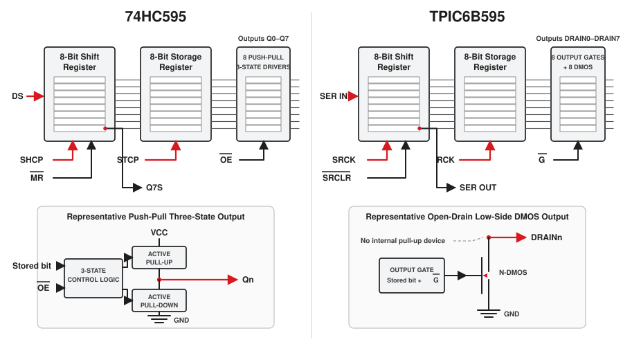
The 74HC595 and TPIC6B595 both convert a serial bit stream into eight latched outputs, but their output stages serve different electrical loads. A 74HC595 provides push-pull logic outputs that can source and sink modest current near its logic supply rails. The TPIC6B595 provides eight open-drain, low-side DMOS switches intended to sink current from higher-voltage or higher-current loads.
The shared "595" architecture does not make the devices pin-compatible or electrically interchangeable. A 74HC595 normally suits logic signals, low-current indicators and control inputs. A TPIC6B595 suits relays, solenoids, lamps and LED loads that connect between a positive load supply and a switched drain. Replacing one with the other requires changes to the footprint, load wiring, signal-level design and firmware polarity.
74HC595 vs TPIC6B595 at a Glance
| Design point | 74HC595 | TPIC6B595 | Practical consequence |
|---|---|---|---|
| Core architecture | 8-bit shift register, 8-bit storage register and eight three-state outputs | 8-bit shift register, 8-bit storage register and eight gated power outputs | Both accept a byte serially and publish it with a separate register-clock edge. |
| Output stage | Push-pull CMOS | Open-drain low-side DMOS | The 74HC595 can source or sink. The TPIC6B595 can only pull a drain toward ground. |
| Representative logic supply | 2.0 V to 6.0 V for Nexperia 74HC595 devices | 4.5 V to 5.5 V | The TPIC6B595 is a 5 V logic device and cannot be powered as a 3.3 V part. |
| Load-voltage domain | Outputs switch within GND to VCC | Drain-to-source rating of 50 V | The TPIC6B595 can control loads powered above its 5 V logic supply when voltage and transient margins are valid. |
| Output-current class | Logic-load current; guaranteed drive depends on manufacturer, VCC and temperature | 150 mA continuous drain-current rating per output under stated conditions | Neither the 74HC595 absolute maximum nor the TPIC headline rating should be used without simultaneous-channel and thermal checks. |
| Inductive-load protection | No integrated power-output clamp | Integrated output clamp; 30 mJ single-pulse avalanche-energy rating | TPIC6B595 is designed for inductive switching, although repetitive energy, release time and EMC still require validation. |
| Package | Commonly 16 pins | 20-pin SOIC or PDIP | The devices are not footprint-compatible. |
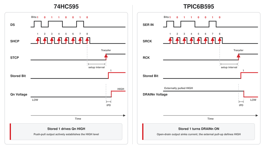
| Bit value at an active load | A stored 1 drives the output HIGH | A stored 1 turns the DMOS channel ON and pulls the drain LOW | The voltage observed at the load node has opposite polarity. |
The figures above are family-level selection references. A production comparison must use the data sheets for the exact manufacturer and suffix. The 74HC595 pinout and timing guide covers the standard logic device in more detail.
What the Two Devices Have in Common
Each device contains an 8-stage serial shift register followed by an 8-bit storage register. One clock advances serial data through the shift register. A second clock transfers the completed byte into storage so all eight external channels update together. Serial data can therefore be shifted while the previous output word remains active.
| Function | Common 74HC595 name | TPIC6B595 name | Behavior |
|---|---|---|---|
| Serial data input | DS or SER | SER IN | Data bit presented before the rising shift-clock edge. |
| Shift clock | SHCP or SRCLK | SRCK | Rising edge shifts one bit into the serial register. |
| Storage/register clock | STCP or RCLK | RCK | Rising edge copies the shift-register word into the storage register. |
| Shift-register clear | MR̅ or SRCLR̅ | SRCLR̅ | LOW clears the shift register; the stored output word does not change until the register clock rises. |
| Output enable | OE̅ | G̅ | HIGH disables the external output stages without erasing either register. |
| Cascade output | Q7S or QH′ | SER OUT | Serial data from the final shift stage feeds the next device. |
The control sequence is nearly identical: hold the register clock steady, present each bit, pulse the shift clock eight times, then apply one rising edge to the register clock. Similar firmware timing is useful during migration, but signal names must be mapped by function rather than assumed from pin position.
The Output Stage Is the Deciding Difference
74HC595: Push-Pull Logic Outputs
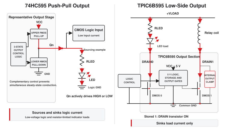
A 74HC595 output contains an active pull-up device and an active pull-down device. A stored 1 drives the pin toward VCC; a stored 0 drives it toward ground. OE̅ HIGH disconnects both devices and places the output in a high-impedance state.
This output structure can drive CMOS inputs, chip-select lines, low-current indicator LEDs and similar logic-domain loads. Output voltage degrades as current increases, so the guaranteed VOH and VOL rows establish the usable current. For example, Texas Instruments specifies approximately ±6 mA test currents for SN74HC595 outputs at a 4.5 V supply while maintaining defined output levels. The much larger current numbers in an absolute-maximum table are stress limits, not normal operating targets.
TPIC6B595: Open-Drain Low-Side Power Outputs
Each TPIC6B595 drain is the output of a power DMOS transistor whose source is internally connected to ground. When its stored bit is 1 and G̅ is LOW, the transistor turns on and sinks current. When the stored bit is 0 or G̅ is HIGH, the transistor turns off. The IC has no active pull-up path on DRAIN0 through DRAIN7.
An off drain may rise through the connected load or an external pull-up, but that voltage is supplied externally. High impedance is not a generated logic HIGH. This distinction is critical when the receiving circuit needs a defined rising edge, a strong HIGH drive or a bidirectional bus.
Correct Load Connections
A 74HC595 load normally sits within the same low-voltage logic domain. An LED may be connected for sourcing or sinking, with one current-limiting resistor per LED. Logic inputs connect directly only when their voltage thresholds, startup states and current requirements are compatible.
A TPIC6B595 load connects from the positive load supply to a DRAIN output. The current path when active is:
The logic supply and load supply may have different voltages, but their grounds must share the required reference unless the interface includes galvanic isolation. The load current does not flow through the TPIC6B595 VCC pin; it returns through the device's ground pins. PCB copper, connectors, ground routing and the load supply must carry the sum of simultaneously active channels.
LED Resistor Calculation with a TPIC6B595
The drain transistor introduces an on-state voltage that must be included in the LED resistor calculation:
For a 12 V supply, a 2.0 V LED and 20 mA target current, an assumed 5 Ω on-resistance gives about 0.10 V across the drain transistor. The calculated resistance is 495 Ω, so 510 Ω is a suitable next standard value. Resistor dissipation is approximately 0.20 W; voltage tolerance, LED forward-voltage spread and ambient temperature should be included before selecting its power rating.
The Aetrix LED resistor calculator can check the resistor and its power. For a TPIC6B595 circuit, use the effective source voltage after subtracting the worst-case drain voltage, then verify the result against the complete current and temperature range.
Current Rating and Thermal Design
Texas Instruments lists 150 mA continuous drain current per TPIC6B595 output, a 50 V output rating and a 500 mA typical current limit at a 25 °C case temperature. The 500 mA figure is a protection characteristic, not a recommended continuous load. The available current falls as the number of conducting outputs and device temperature increase.
DMOS conduction loss for one active channel is approximated by:
Using 5 Ω as an initial estimate, one channel at 100 mA dissipates about 0.05 W. Eight identical channels continuously active would contribute about 0.40 W before logic and switching losses. At higher temperature the on-resistance rises; TI specifies higher maximum resistance under hot conditions, so a room-temperature typical value is unsuitable for a worst-case thermal sign-off.
Junction temperature can be screened with:
This estimate depends strongly on the package, PCB copper, airflow and measurement conditions. The Aetrix power dissipation and thermal calculator can provide an initial temperature-rise check. Enter an equivalent on-state drop of ID × RDS(on), apply the correct duty cycle, and use the thermal data for the selected package and PCB environment. Final validation still requires worst-case data-sheet limits and hardware temperature measurements.
- Sum the losses from every output that can conduct at the same time.
- Use maximum RDS(on) at the relevant temperature when establishing worst-case margin.
- Keep load-current loops short and use sufficient copper for the drain and ground paths.
- Do not route high-current ground return through a narrow logic-ground trace.
- Check connector, via and PCB-trace current capacity as well as IC dissipation.
Driving Relays, Solenoids and Other Inductive Loads
The TPIC6B595 includes an output clamp and a 30 mJ single-pulse avalanche-energy rating. When a channel switches off, energy stored in the coil forces the drain voltage upward. The clamp limits that rise by allowing the output transistor to absorb the inductive energy.
Coil energy must stay within the applicable avalanche limits after allowance for component tolerance, supply variation, starting junction temperature, repetition rate and the number of channels releasing together. A repetitive relay bank cannot be approved from the 30 mJ headline value alone.
An external flyback diode or TVS may still be appropriate. A diode usually produces a slower current decay and longer relay release time. A higher-voltage clamp speeds release but increases electrical stress and radiated or conducted noise. Contact requirements, release timing, EMC and thermal load determine the protection network.
A 74HC595 normally needs a separate transistor or MOSFET for each inductive channel plus a correctly placed flyback path. Its logic-output protection structures are not substitutes for an inductive-load driver.
3.3 V Microcontroller Compatibility
A 74HC595 powered from 3.3 V can usually connect directly to a 3.3 V microcontroller when both data sheets provide compatible VOH, VOL, VIH and VIL limits. A 5 V-powered HC device needs a separate threshold check because its CMOS HIGH threshold rises with VCC.
The TPIC6B595 has a recommended VCC range of 4.5 V to 5.5 V. Its specified HIGH input threshold is 0.85 × VCC and its LOW threshold is 0.15 × VCC. At VCC = 5.0 V, the guaranteed HIGH input is therefore at least 4.25 V. A 3.3 V GPIO does not meet that requirement.
Use a unidirectional level translator or a suitable 5 V HCT/AHCT buffer between a 3.3 V controller and SER IN, SRCK, RCK, SRCLR̅ and G̅ as required. The translator must produce valid 5 V logic levels and preserve clock-edge quality. Power sequencing also matters: do not allow a powered controller to drive unpowered logic inputs beyond their permitted limits.
Pinout and PCB Differences
The common 74HC595 uses a 16-pin footprint. TPIC6B595 uses a 20-pin SOIC or PDIP footprint with multiple ground pins, eight drain outputs and two no-connect pins. No pin-for-pin board substitution is possible.
| TPIC6B595 pin group | Pin number | Connection |
|---|---|---|
| VCC | 2 | Regulated 4.5 V to 5.5 V logic supply with local ceramic bypassing. |
| SER IN | 3 | Serial data input. |
| DRAIN0–DRAIN3 | 4–7 | First four low-side DMOS load outputs. |
| SRCLR̅ | 8 | Active-LOW shift-register clear; hold HIGH during normal shifting. |
| G̅ | 9 | Active-LOW output enable; HIGH turns all drains off. |
| GND | 10, 11 and 19 | Logic and power-output return. Connect all ground pins with low impedance. |
| RCK | 12 | Storage-register clock; data transfers on the rising edge. |
| SRCK | 13 | Shift-register clock; SER IN is sampled on the rising edge. |
| DRAIN4–DRAIN7 | 14–17 | Remaining four low-side DMOS load outputs. |
| SER OUT | 18 | Serial cascade output from the final shift stage. |
| NC | 1 and 20 | No internal connection; do not treat these pins as grounds or thermal terminals. |
Place the bypass capacitor close to VCC and the ground network. Give the three ground pins a short connection into the ground plane. Drain traces should be sized for load current, and their return paths should avoid adding voltage to the logic reference used by the input thresholds.
Output Enable, Clear and Safe Startup
Output enable and register clear solve separate problems on both devices. OE̅ or G̅ disables the external drivers but retains the stored word. MR̅ or SRCLR̅ clears the shift register but leaves the storage register unchanged until a storage-clock edge transfers the cleared word.
A controlled TPIC6B595 startup can use the following order:
- Hold G̅ HIGH so every drain output remains off.
- Hold RCK LOW and pulse SRCLR̅ LOW for the required clear interval.
- Return SRCLR̅ HIGH.
- Apply one rising edge to RCK to copy the cleared word into storage.
- Drive G̅ LOW only after the output word and load supply are safe.
Pull resistors should establish these levels while the microcontroller is resetting or disconnected. Avoid an RC network on a clock input unless its edge rate remains within the input requirements; a slow or noisy transition can create unintended clocking.
Cascading and Mixed-Device Chains
Multiple 74HC595 devices cascade by connecting the final shift-stage output of one device to the serial input of the next. TPIC6B595 uses the same principle: SER OUT connects to SER IN of the following device while SRCK and RCK are shared. A chain of N devices requires 8N shift-clock edges before the register clocks update the outputs.
A mixed 74HC595 and TPIC6B595 chain is possible only when every inter-device voltage and timing limit is satisfied. A 3.3 V-powered 74HC595 serial output does not meet the TPIC6B595 5 V HIGH-input requirement. A 5 V TPIC6B595 SER OUT may exceed the input rating of a downstream 3.3 V logic device. Shared clocks from a 3.3 V controller also need translation before they reach the TPIC6B595.
Separate chains are often easier to validate because the logic-voltage domains, output polarity and safety controls remain independent. If the chains are combined, document the bit order and whether a stored 1 means "pin HIGH" or "load energized" for every byte position.
Which Device Fits the Load?
| Load or system requirement | Preferred starting point | Reason |
|---|---|---|
| CMOS logic inputs or chip-select lines | 74HC595 | Push-pull HIGH and LOW drive with logic-domain voltage levels. |
| Several low-current indicator LEDs | 74HC595 | Compact 16-pin solution when resistor, output-voltage and total-current limits are satisfied. |
| 12 V or 24 V LED indicators | TPIC6B595 | Open-drain outputs can sink current from a separate higher-voltage load rail. |
| Relay or solenoid bank within current and energy limits | TPIC6B595 | Power DMOS sinks and integrated clamp support low-side inductive switching. |
| Load requires current sourcing from the positive rail | Neither as a direct TPIC6B595 replacement | TPIC6B595 only sinks; use a suitable high-side or source-driver architecture. |
| Bidirectional or shared digital bus | Neither without a system-level check | Both are output expanders; the TPIC drains are not push-pull logic outputs. |
| 3.3 V system with no level translator | 3.3 V-compatible 74HC595 | TPIC6B595 requires a 4.5 V to 5.5 V logic supply and higher HIGH-level inputs. |
Why TPIC6B595 Is Not a Drop-In 74HC595 Replacement
- The package changes from the usual 16-pin 74HC595 layout to a 20-pin TPIC6B595 layout.
- The eight Q outputs become open-drain DRAIN outputs.
- The TPIC6B595 cannot source current or generate a HIGH output voltage.
- The logic supply and input thresholds may require a 5 V rail and level translation.
- The load must be rewired between its positive supply and the drain.
- A stored 1 energizes a low-side TPIC channel, so external node polarity changes.
- Power dissipation, ground current, inductive energy and PCB copper become load-design parameters.
For an existing 74HC595 board that needs more current, adding an external transistor array may require fewer firmware changes than replacing the shift register. A new design with multiple high-voltage sink loads can use TPIC6B595 to combine the serial register, storage register and low-side drivers in one device. Cost, board area, load current, fault behavior and component availability determine which architecture is cleaner.
Troubleshooting a TPIC6B595 Conversion
| Observed behavior | Likely cause | Engineering check |
|---|---|---|
| TPIC6B595 does not recognize 3.3 V control signals | Input HIGH voltage is below 0.85 × VCC. | Measure the signal at the IC pin and add a specified 3.3 V-to-5 V translator. |
| Load turns on when software expects a LOW output | Open-drain polarity was interpreted like a push-pull output. | Define a stored 1 as "drain ON" and verify byte polarity with one channel connected. |
| Drain never rises when the channel turns off | No pull-up or load path exists, or the external wiring holds the node low. | Trace the current path from +VLOAD through the load to DRAINn. |
| Outputs remain in the previous state after SRCLR̅ | Only the shift register was cleared. | Return SRCLR̅ HIGH and pulse RCK to transfer the zero word. |
| Device overheats with several active loads | Simultaneous I²R loss and PCB thermal resistance exceed the temperature budget. | Measure channel current, calculate total loss with hot RDS(on), and inspect ground and copper temperature. |
| Relay switching resets the controller | Load-current return, supply dip or inductive transient is disturbing the logic domain. | Probe VCC and ground at both ICs; separate current loops and review clamp or flyback paths. |
| One bit shifts to the wrong channel | Bit order, cascade path or final-clock timing is incorrect. | Run a walking-one pattern and probe SER IN, SRCK, RCK and SER OUT. |
Part Number and Procurement Checks
A complete comparison should include the manufacturer and full ordering code. "74HC595" covers implementations from several logic suppliers, with differences in guaranteed drive, timing, temperature range, package and qualification. TPIC6B595 variants include 20-pin surface-mount and through-hole packages with different packing suffixes.
- Confirm whether the required output is push-pull, open-drain sink or high-side source.
- Specify logic VCC, load voltage, continuous current, peak current and simultaneous active-channel count.
- For inductive loads, specify coil inductance, current, switching frequency and required release time.
- Match the package drawing and land pattern; a shared functional description does not establish footprint compatibility.
- Check operating-temperature limits and automotive qualification separately.
- Preserve the exact manufacturer suffix when reel format, lead finish, qualification or traceability matters.
Aetrix lists Texas Instruments SN74HC595DR, Nexperia 74HC595D,118 and other devices in the shift-register category. For TPIC6B595 package options or a production comparison, provide the full part number, quantity, load requirements and required date through the Aetrix RFQ page.
Technical References
- Texas Instruments TPIC6B595 power logic 8-bit shift register data sheet
- Texas Instruments SN54HC595 / SN74HC595 data sheet
- Nexperia 74HC595 / 74HCT595 product information
Frequently Asked Questions
What is the main difference between 74HC595 and TPIC6B595?
The 74HC595 has push-pull logic outputs that source and sink modest current within its logic supply range. The TPIC6B595 has open-drain low-side DMOS outputs that sink current from externally powered loads.
Is TPIC6B595 a drop-in replacement for 74HC595?
No. TPIC6B595 uses a 20-pin package, a 5 V logic supply and open-drain power outputs. A common 74HC595 uses a 16-pin package and push-pull logic outputs. The footprint, load wiring, voltage interface and firmware polarity must be reviewed.
Can TPIC6B595 drive relays directly?
It can drive low-side relay coils when the coil voltage, current, stored energy, switching rate, simultaneous-channel load and junction temperature remain within the specified limits. The load connects from its positive supply to a drain output.
Can a 3.3 V microcontroller drive TPIC6B595 directly?
Not as a guaranteed interface. With VCC at 5.0 V, the TPIC6B595 specified HIGH threshold is 4.25 V. Use a suitable level translator or 5 V HCT/AHCT buffer for the required control signals.
Can TPIC6B595 source current?
No. Its power outputs are open-drain low-side switches. They can pull a connected load toward ground but cannot actively drive a drain HIGH or supply current from the positive rail.
Can all eight TPIC6B595 outputs continuously sink 150 mA?
The device lists a 150 mA continuous rating per output under stated conditions, but an eight-channel design must also satisfy the simultaneous-current curves, RDS(on), total power dissipation, case or ambient temperature and PCB thermal conditions. Treating 8 × 150 mA as an unconditional operating point is unsafe.
Why does a TPIC6B595 drain read HIGH when the output is off?
The drain is high impedance when its DMOS transistor is off. The connected load or pull-up raises the drain voltage. The TPIC6B595 itself does not source that HIGH level.
Does SRCLR̅ immediately turn off the TPIC6B595 loads?
No. SRCLR̅ clears the shift register, while the storage register retains its previous word. After SRCLR̅ returns HIGH, a rising RCK edge is required to transfer zeros into storage. G̅ can disable all drains immediately while remaining HIGH.


