
 My Inquiry
 My Account


74HC595 Pinout, Timing, Output Current, and Applications
Article Details
The 74HC595 is an 8-bit serial-in, parallel-out shift register with a second 8-bit storage register and three-state output drivers. Serial data enters through DS, advances one position on each rising edge of SHCP, and reaches the parallel outputs only when a rising edge on STCP transfers the completed byte into the storage register.
The separate shift and storage clocks are the feature that makes the device useful for output expansion. A microcontroller can load eight new bits while Q0 through Q7 continue driving the previous word. One STCP edge then updates all eight outputs together. Three controller signals-data, shift clock and storage clock-are therefore enough for eight outputs, and additional devices can be cascaded without adding another data pin.
What Is Inside a 74HC595?
The device contains three functional sections. The first is an 8-stage shift register that samples DS on rising SHCP edges. The second is an 8-bit storage register loaded on a rising STCP edge. The third is a bank of eight three-state drivers controlled by OE̅. Q7S is taken from the final shift stage and provides the serial data needed to extend the chain.
The word "latch" appears in many 74HC595 descriptions, although the storage section is updated by an edge rather than remaining transparent for an enable level. The timing distinction is covered in the latch-versus-flip-flop comparison. The wider relationship between storage, feedback and controlled data transfer is also described in the latch circuit reference.
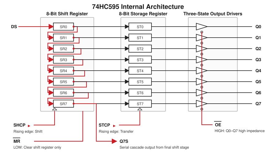
| Internal section | Controlling signal | What changes | What remains unchanged |
|---|---|---|---|
| 8-bit shift register | SHCP rising edge | DS enters the first stage and existing bits move toward Q7S. | The storage register and Q0–Q7 retain their previous word. |
| 8-bit storage register | STCP rising edge | All eight shift-register bits are copied into storage. | The shift register can continue holding or shifting its own data. |
| Three-state output drivers | OE̅ level | LOW enables Q0–Q7; HIGH places them in high impedance. | Neither internal register is cleared or modified. |
| Asynchronous shift clear | MR̅ LOW | All shift-register stages become zero. | The stored output word is unchanged until STCP rises. |
74HC595 Pinout and Signal Functions
The familiar 16-pin pinout is shared by many HC and HCT implementations, but the exact package drawing and signal notation should always be checked for the selected manufacturer. Nexperia commonly uses DS, SHCP, STCP, MR̅, OE̅ and Q7S. Texas Instruments uses SER, SRCLK, RCLK, SRCLR̅, OE̅ and QH′ for the corresponding signals.
| Pin | Common name | TI equivalent | Function and design treatment |
|---|---|---|---|
| 1 | Q1 | QB | Stored parallel output bit 1; high impedance while OE̅ is HIGH. |
| 2 | Q2 | QC | Stored parallel output bit 2. |
| 3 | Q3 | QD | Stored parallel output bit 3. |
| 4 | Q4 | QE | Stored parallel output bit 4. |
| 5 | Q5 | QF | Stored parallel output bit 5. |
| 6 | Q6 | QG | Stored parallel output bit 6. |
| 7 | Q7 | QH | Stored parallel output bit 7. |
| 8 | GND | GND | Ground reference. Connect to a low-impedance return and place the bypass capacitor close to pins 16 and 8. |
| 9 | Q7S | QH′ | Serial output from the final shift stage. Connect to DS/SER of the next device when cascading. |
| 10 | MR̅ | SRCLR̅ | Asynchronous active-LOW clear for the shift register. Hold HIGH during normal operation; never leave it floating. |
| 11 | SHCP | SRCLK | Shift-register clock. DS is sampled on its LOW-to-HIGH transition. |
| 12 | STCP | RCLK | Storage-register clock. A rising edge transfers the eight shift bits to Q0–Q7. |
| 13 | OE̅ | OE̅ | Active-LOW output enable. Tie LOW for permanently driven outputs or control it with a defined logic signal. |
| 14 | DS | SER | Serial data input. It must meet setup and hold timing around the SHCP rising edge. |
| 15 | Q0 | QA | Stored parallel output bit 0. |
| 16 | VCC | VCC | Positive supply. Use local decoupling and verify the voltage range of the exact logic family. |
For a basic always-enabled circuit, MR̅ is normally pulled or tied HIGH and OE̅ is tied LOW. Direct ties are acceptable only when the system never needs blanking, bus release or controlled startup. Inputs driven by a microcontroller can be unsafe during reset if its pins become high impedance, so pull resistors may still be required to establish known levels.
How Data Moves Through the 74HC595
Assume the shift register is initially zero and eight bits are sent most-significant bit first. The first transmitted bit enters stage Q0 on the first SHCP rising edge, then moves one stage toward Q7 on every later edge. After eight clocks, the first transmitted bit has reached Q7 and the last transmitted bit occupies Q0. A different software bit order changes the relationship between the byte value and the physical output pins; it does not change the internal shift direction.
- Hold MR̅ HIGH and OE̅ at the desired output state.
- Keep STCP from making a rising transition while the new word is being shifted.
- Set DS to the next bit and allow it to settle before SHCP rises.
- Pulse SHCP HIGH and LOW once for each bit.
- After the final shift edge and the required separation time, apply one rising edge to STCP.
- Q0–Q7 change after the STCP-to-output propagation delay.
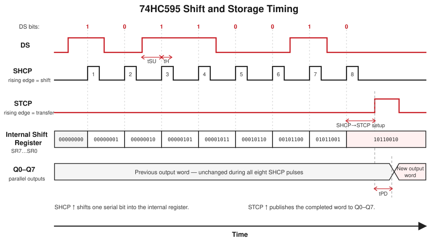
SHCP and STCP Are Separate Clock Domains Inside the Device
Both inputs are positive-edge triggered, but they perform different operations. SHCP moves the serial pipeline by one bit. STCP copies a complete internal snapshot to the output register. Keeping the signals separate gives the controller a clean update boundary and prevents intermediate shift states from appearing at the load.
The final SHCP edge and the STCP edge should not be placed arbitrarily close together. The shift-register contents need time to settle before the storage register captures them. As one concrete reference, the TI SN74HC595 timing table at VCC = 4.5 V specifies a 19 ns minimum SRCLK-rising-to-RCLK-rising setup interval across the SN74HC595 operating range. It also guarantees 25 MHz clock operation and specifies 20 ns minimum clock HIGH and LOW pulse widths plus 25 ns SER setup time under that condition. Values differ with supply voltage, load, temperature, manufacturer and logic-family revision.
SHCP and STCP can be tied together in applications that accept a one-clock pipeline relationship. In that configuration, the shift register remains one clock ahead of the storage register. Most microcontroller output-expansion circuits keep them separate because a dedicated STCP signal provides an explicit, glitch-controlled parallel update.
MR̅ and OE̅ Solve Different Problems
Pulling MR̅ LOW immediately clears the eight shift stages. It does not directly erase the storage register. If Q0–Q7 currently display a nonzero word, that word stays present while OE̅ is LOW until STCP rises and copies the cleared shift register into storage.
Driving OE̅ HIGH disconnects Q0–Q7 electrically by placing them in the high-impedance state. The shift and storage registers keep their data. OE̅ can blank a display, release a shared bus or hold external loads inactive during startup, but it cannot substitute for loading a safe output word.
| Event or level | Shift register | Storage register | Q0–Q7 |
|---|---|---|---|
| SHCP rises with MR̅ HIGH | Shifts; DS enters the first stage | No change | No change if OE̅ is LOW; high impedance if OE̅ is HIGH |
| STCP rises | No change | Copies all eight shift stages | Updates after propagation delay when OE̅ is LOW |
| MR̅ is LOW | Cleared asynchronously | No change | Retains stored word until a later STCP edge |
| OE̅ is HIGH | Normal shifting remains possible | Normal loading remains possible | High impedance |
74HC595 Operating Video
Video: "The Shift Register: Explained [74HC595]" by electronica.
74HC595 Output Current: Use the Guaranteed Logic Levels
Output-current design starts with the VOH and VOL tables, not the absolute maximum section. Current drawn from a HIGH output lowers VOH; current sunk by a LOW output raises VOL. The load must still receive a valid voltage after that drop, and the total current through the package supply pins must remain within its limit.
For example, TI specifies its SN74HC595 parallel outputs at approximately ±6 mA with VCC = 4.5 V while maintaining guaranteed output levels. The same data sheet lists ±35 mA continuous current for one output and ±70 mA through VCC or GND under absolute maximum ratings. Those larger figures are stress limits. Continuous operation near them is outside the recommended design conditions and leaves no useful logic-level, thermal or simultaneous-switching margin.
| Current figure | Correct interpretation | Design consequence |
|---|---|---|
| Guaranteed IOH/IOL test current | Current at which the manufacturer guarantees a stated VOH or VOL. | Use this row to check logic loads and low-current indicators. |
| Per-output absolute maximum | Stress boundary that prevents immediate damage under specified conditions. | Do not use it as normal LED, relay or actuator drive current. |
| VCC/GND total-current limit | Aggregate current for all simultaneously active outputs and internal supply current. | Eight channels cannot each consume the single-pin maximum. |
| Package power dissipation | Heat generated by output voltage drop, switching and quiescent current. | Check ambient temperature, package thermal data and simultaneous loading. |
Choosing LED Resistors
Every LED needs its own series resistor. For a LOW-side connection in which the 74HC595 sinks current, a first calculation is:
For a HIGH-side connection in which the output sources current, use the guaranteed loaded VOH rather than assuming that the output remains exactly at VCC:
After choosing a resistor, check every simultaneously illuminated channel against the total device current and package dissipation. Multiplexed displays also require peak-current and duty-cycle calculations. Relays, solenoids, motors, high-current lamps and large LED arrays need external transistor or MOSFET drivers, flyback protection where inductance is present, and a supply path sized for the load.
3.3 V and 5 V Logic Compatibility
A 74HC595 powered at 3.3 V is normally straightforward to drive from a 3.3 V microcontroller when both devices share a valid ground and the selected part supports that supply. Q0–Q7 then produce approximately 3.3 V logic levels, subject to output loading.
A 74HC595 powered at 5 V has CMOS input thresholds that scale with VCC. The TI SN74HC595, for example, specifies VIH = 3.15 V minimum at VCC = 4.5 V. A nominal 3.3 V microcontroller output leaves little margin after tolerance, noise and voltage drop, and a guaranteed interface cannot be assumed across all HC vendors and conditions.
Three common solutions are available:
- Power the HC device from 3.3 V if the loads accept 3.3 V output levels.
- Use a 74HCT595 at approximately 5 V when TTL-compatible input thresholds suit the controller interface.
- Insert a level translator when voltage domains, edge quality or power sequencing require explicit isolation.
Input overvoltage tolerance and clamp structures vary between logic families and manufacturers. A series resistor does not automatically make every HC595 input safe at a voltage above VCC. Verify the input-voltage rating, injection-current limit and power-off behavior of the exact part.
Cascading Multiple 74HC595 Devices
Connect Q7S of the first device to DS of the second. Share SHCP and STCP across the chain. MR̅ and OE̅ may also be shared when every device must clear or release its outputs together. A chain of N devices requires 8N shift-clock edges before a single STCP edge updates all outputs.
The formula covers bit transfer only. Firmware overhead, STCP pulse timing and the required setup interval add to the update time. Long chains also increase clock-line capacitance and make Q7S propagation delay, trace ringing, ground bounce and connector quality more important.
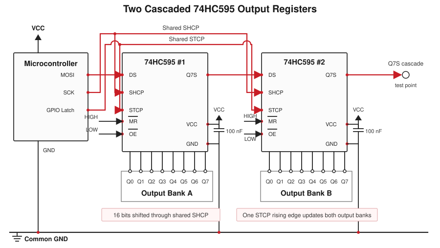
There is no universal maximum device count. The practical limit is reached when the controller cannot shift the required word within the update interval, the last Q7S-to-DS path violates setup time, or clock and supply integrity no longer meet the data-sheet conditions. Buffering a heavily loaded clock, slowing the edge rate with a carefully selected source resistor, improving ground return and distributing decoupling are more useful than relying on an arbitrary chain-length rule.
SPI Connection
Hardware SPI can drive the serial path efficiently. Connect MOSI to DS and SCK to SHCP, then use a separate GPIO for STCP. Select a mode in which MOSI is stable before the rising SCK edge; SPI mode 0 is a common choice. OE̅ and MR̅ can be fixed at safe levels or assigned to extra GPIOs when blanking and hardware clear are required.
set_output_enable(HIGH);     // Q0-Q7 high impedance during startup
set_master_reset(LOW);      // clear the shift register
wait_minimum_reset_pulse();
set_master_reset(HIGH);
pulse_storage_clock();      // transfer zeros into output storage
set_output_enable(LOW);     // drive the known all-zero word

spi_write(next_output_byte); // DS is sampled on each SHCP rising edge
wait_required_clock_spacing();
pulse_storage_clock();       // update all eight outputs together
The bit order must match the board net names. If software sends the most-significant bit first, the first bit normally ends at Q7 after eight shifts and the final bit remains at Q0. A one-hot walking-bit test is the quickest way to verify physical mapping before loads are energized.
Power, Layout and Startup Design
- Place a 100 nF ceramic capacitor close to VCC and GND for each 74HC595. The connection loop should be short and should not share a narrow return path with high-current loads.
- Give SHCP and STCP continuous ground references. Fast logic edges can ring even when the nominal clock frequency is modest.
- Hold MR̅, OE̅, SHCP and STCP at defined levels while the controller is resetting. Floating CMOS inputs can cause extra clock edges and unpredictable outputs.
- Keep OE̅ HIGH during power-up when external loads must remain inactive, then clear and latch a known word before enabling the outputs.
- Route inductive or high-current load return current away from the logic ground path. External drivers should include the protection required by the load.
- For cables or long board traces, verify edge integrity at the receiving pins with an oscilloscope. Count threshold crossings rather than judging only the apparent clock frequency.
Common 74HC595 Applications and Their Limits
| Application | Useful 74HC595 function | Important limitation |
|---|---|---|
| Status LEDs and seven-segment displays | Eight stable outputs with an atomic STCP update; OE̅ can provide global blanking or PWM. | Use one resistor per LED and check aggregate current. OE̅ controls all channels together. |
| Microcontroller GPIO expansion | Three controller signals create eight or more write-only outputs. | The device provides no input readback, interrupt function or per-pin direction control. |
| Relay and solenoid control | Latched control word prevents partial updates during serial loading. | External drivers and flyback paths are required; the HC output stage is not a relay driver. |
| Chip-select or mode-control banks | One STCP edge changes a complete control word. | Power-up state and brief update transitions must be safe for every controlled device. |
| Cascaded display columns | Q7S permits long serial chains with shared clocks. | Refresh time, duty cycle, clock loading and simultaneous switching set the usable scale. |
74HC595, 74HCT595 and Other Shift Registers
| Device family | Main distinction | Selection guidance |
|---|---|---|
| 74HC595 | CMOS input thresholds and a broad supply range on common implementations. | Use when the controlling logic levels satisfy HC thresholds at the chosen VCC. |
| 74HCT595 | TTL-compatible inputs, commonly specified around a 5 V supply. | Useful for a 3.3 V-to-5 V control interface when the exact VIH and supply specifications are met. |
| 74AHC595 / 74AHCT595 | Faster family with different switching and input characteristics. | Recheck signal integrity, overvoltage tolerance, timing and package before substitution. |
| 74HC164 | Serial-in/parallel-out shift register without the separate 595-style output storage register or three-state bank. | Its parallel outputs change while data shifts, so it does not provide the same glitch-controlled update. |
| TPIC6B595-class driver | Power-oriented open-drain low-side outputs for higher-current loads. | Output polarity, voltage, current, pinout and load connection differ; treat it as a new circuit design. |
Nexperia lists 74HC595 and 74HCT595 options in SO16, TSSOP16 and leadless packages. Aetrix product pages include the 74HC595D,118 in SO16, 74HC595PW,118 in TSSOP16 and 74HC595BQ,115 in DHVQFN16. Package code, temperature grade, packing suffix and qualification status belong to the complete orderable number and should be checked independently.
The broader shift-register category includes serial-to-parallel and parallel-to-serial devices with different control structures. Parts that share "8-bit shift register" in their descriptions are not automatically pin-compatible or functionally equivalent.
Troubleshooting Common 74HC595 Problems
| Observed problem | Likely cause | Engineering check |
|---|---|---|
| Outputs change while bits are being sent | STCP is receiving unintended rising edges, or the circuit uses a device without a separate storage register. | Probe SHCP and STCP together and confirm the exact IC marking and pinout. |
| MR̅ does not clear visible outputs | Only the shift register has been cleared. | Pulse STCP after MR̅ returns HIGH to transfer the cleared word. |
| All outputs remain inactive | OE̅ is HIGH, floating or controlled with reversed polarity. | Measure pin 13 at the device and verify that LOW enables the outputs. |
| Random state appears at power-up | Storage contents and control inputs were not initialized before outputs were enabled. | Hold OE̅ HIGH, clear the shift register, pulse STCP, then enable outputs. |
| 5 V device responds intermittently to 3.3 V control | HC input HIGH margin is inadequate. | Compare the controller VOH minimum with the shift register VIH minimum across voltage and temperature. |
| Errors occur when many loads switch | Supply droop, ground bounce, excessive package current or insufficient decoupling. | Probe VCC at the IC, reduce load current and separate load-return current from logic ground. |
| A cascaded chain loses or shifts one bit | Q7S is connected to the wrong node, bit order is wrong, or setup time is violated at the next DS input. | Run a walking-one pattern and probe Q7S, DS and SHCP at the final device. |
Package and Procurement Checks
A complete 74HC595 order review should include manufacturer, logic family, package drawing, temperature range, qualification, tape orientation and packing suffix. HC, HCT, AHC, AHCT, LV and LVC versions can differ in supply range, thresholds, speed, overvoltage behavior and output drive even when their functional block diagrams look similar.
- Match the land pattern to the exact package drawing; SO16, TSSOP16 and DHVQFN16 footprints are not interchangeable.
- Confirm whether automotive qualification is required instead of assuming that a −40 °C to +125 °C rating establishes qualification.
- Check the manufacturer's lifecycle status for the exact suffix, not only the generic 74HC595 family name.
- For cross-manufacturer replacement, compare VIH/VIL, VOH/VOL at load, timing limits, pin functions, power-off behavior and package dimensions.
- Use traceability, packaging inspection and electrical testing appropriate to the sourcing channel and application risk.
For production quantities or a multi-manufacturer comparison, submit the full part number, package, required temperature range and annual demand through the Aetrix RFQ page. Those details prevent a functionally similar device in the wrong logic family or footprint from being treated as a direct substitute.
Technical References
- Nexperia 74HC595 / 74HCT595 product and application data
- Texas Instruments SN54HC595 / SN74HC595 data sheet
- Nexperia products at Aetrix Electronics
Frequently Asked Questions
What is a 74HC595 used for?
It converts serial data into eight stable parallel outputs. Common uses include status LEDs, display segments, chip-select banks and write-only microcontroller output expansion.
How many microcontroller pins does one 74HC595 require?
Basic operation requires three signals: DS for data, SHCP for shifting and STCP for the parallel update. OE̅ and MR̅ may be tied to defined levels or controlled with additional pins.
What is the difference between SHCP and STCP?
SHCP shifts one serial bit on each rising edge. STCP copies all eight shift-register bits into the storage register on its rising edge, causing Q0–Q7 to update together.
Does MR̅ immediately clear the 74HC595 outputs?
No. MR̅ clears the shift register asynchronously. The cleared zeros reach Q0–Q7 only after a rising STCP edge transfers them to the storage register, assuming OE̅ is LOW.
Can a 3.3 V microcontroller drive a 5 V 74HC595?
It is not guaranteed for every HC implementation. Compare the controller's minimum VOH with the 74HC595 VIH requirement. A 3.3 V-powered HC device, a 5 V HCT device with TTL-compatible inputs or a level translator may provide a valid interface.
Can the 74HC595 drive eight LEDs directly?
It can drive low-current LEDs when each LED has a resistor and all per-output, total-current, output-voltage and package-power limits are satisfied. High-current LEDs and multiplexed arrays usually require external drivers.
How many 74HC595 devices can be cascaded?
The logic architecture sets no small fixed count. The practical limit depends on the required update rate, Q7S propagation delay, next-device setup time, clock loading, signal integrity, supply distribution and PCB or cable length.
What is the difference between 74HC595 and 74HC164?
The 74HC595 has a separate output storage register and three-state parallel drivers, so outputs can remain stable while a new word shifts in. The 74HC164 exposes its shifting states at the parallel outputs and does not provide the same atomic update.


