
 My Inquiry
 My Account


Latch vs Flip-Flop: Timing, Differences and Design Choices
Article Details
A latch and a flip-flop each store one binary state, but they accept data at different times. A latch is level-sensitive: its input can affect the output throughout an active Enable level. A flip-flop is edge-triggered: it captures data within a narrow timing aperture around a designated clock transition.
That timing distinction changes circuit behavior well beyond the truth table. It determines whether several input transitions can pass during one control phase, where setup and hold checks apply, whether a path can borrow time from the next phase, and how easily data can race through cascaded storage elements.
The underlying latch circuits are covered separately in the latch circuit reference, the SR latch guide and the D latch circuit guide. The comparison here concentrates on timing architecture, device selection and design consequences.
Latch: data can pass for the full active Enable level.
Flip-flop: data is sampled around one active clock edge.
Shared limitation: both require valid setup and hold margins at the point where a new state is captured.
Latch vs Flip-Flop: The Core Difference
| Characteristic | Latch | Flip-flop | Engineering consequence |
|---|---|---|---|
| Control sensitivity | Active control level | Active clock edge | Defines the interval during which D can be accepted. |
| Input-to-output behavior | Q may follow D while the latch is transparent | Q updates after the sampling edge | A latch can pass several input transitions during one active phase. |
| Capture boundary | Edge that closes the transparent window | Specified rising or falling clock edge | Setup and hold constraints use different timing references. |
| Output delay | D-to-Q while open; Enable-to-Q when opening | Clock-to-Q after the active edge | Static timing models use different arcs. |
| Timing flexibility | Can support time borrowing | Uses a fixed edge-to-edge cycle boundary | Latch pipelines can redistribute delay between adjacent stages. |
| Typical failure risk | Race-through or phase-overlap errors | Edge setup/hold failure or clock-skew loss | Clocking strategy and minimum-delay checks differ. |
| Common board-level example | 74HC573 octal transparent latch | 74HC574 octal edge-triggered register | Similar bus roles require different control waveforms. |
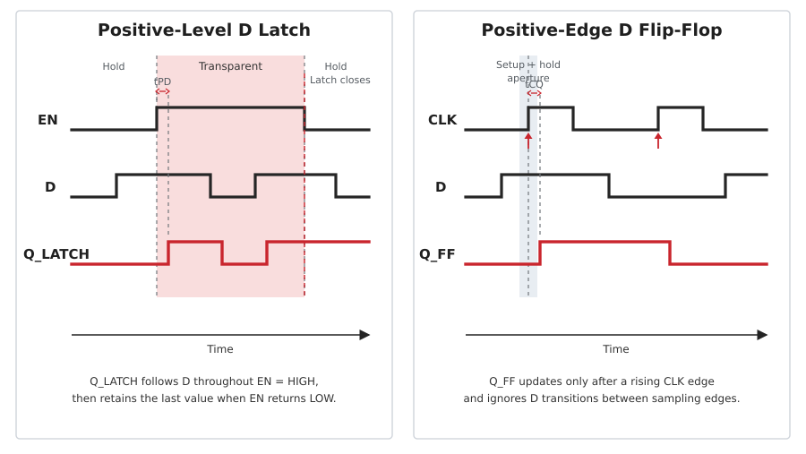
A positive-level D latch is transparent while EN is HIGH and retains data when EN becomes LOW. A positive-edge-triggered D flip-flop samples D around the LOW-to-HIGH transition of CLK. Calling both devices "one-bit memory" is correct, but it does not describe when their stored state can change.
Edge-triggered does not mean instantaneous. The flip-flop still has a finite setup interval before the clock edge, a hold interval after it, and a clock-to-Q delay. The edge represents the reference point for those limits rather than a zero-duration physical event.
Timing Behavior: Transparent Window vs Sampling Edge
Assume the latch and flip-flop receive the same D waveform. While a positive-level latch has EN = HIGH, each valid change at D can reach Q after D-to-Q propagation delay. When EN falls, the transparent window closes and later D transitions are blocked.
A positive-edge flip-flop ignores those between-edge transitions at its stored output. It captures the D value that satisfies setup and hold requirements around the next rising clock edge, then presents that value at Q after clock-to-Q delay. A narrow glitch between clock edges usually has no effect on Q; a glitch inside the sampling aperture can be captured or violate timing.
Latch and Flip-Flop Video Comparison
Video: "Latch and Flip-Flop Explained | Difference between the Latch and Flip-Flop," ALL ABOUT ELECTRONICS.
Setup, Hold and Propagation Timing
For a positive-level latch, setup and hold time are referenced to the falling edge of EN because that transition closes the data path. The rising edge opens the latch and introduces an Enable-to-Q response when D already differs from the stored value. During transparency, D-to-Q delay controls how quickly later data changes appear at Q.
For a positive-edge flip-flop, setup and hold time are referenced to the rising clock edge. Downstream logic begins its timing interval after the corresponding clock-to-Q delay. A negative-edge device uses the falling edge instead, but its storage behavior remains edge-triggered.
| Timing item | Latch reference | Flip-flop reference | Common design error |
|---|---|---|---|
| Setup time | D stable before the latch-closing edge | D stable before the active clock edge | Checking the latch only at the opening edge |
| Hold time | D stable after the latch-closing edge | D stable after the active clock edge | Ignoring a short-path change immediately after capture |
| Output propagation | D-to-Q while transparent or EN-to-Q when opening | Clock-to-Q after the active edge | Applying a flip-flop delay model to a transparent latch |
| Minimum control width | Minimum open and closed Enable intervals | Minimum HIGH and LOW clock pulse widths | Assuming a narrow pulse is accepted because logic levels are valid |
| Metastability exposure | Data changes near the closing edge | Data changes near the sampling edge | Treating an asynchronous input as safe because the device is edge-triggered |
A setup or hold violation can make either element resolve late or store an unpredictable value for that event. A clean digital simulation may hide the analog regeneration interval unless the cell model includes timing checks. Synchronizer design, clock-domain crossing analysis and sufficient settling time remain necessary when asynchronous signals enter either architecture.
How Two Latches Form an Edge-Triggered Flip-Flop
A master–slave D flip-flop can be built from two level-sensitive latches controlled by opposite clock phases. In a positive-edge arrangement, the master latch is transparent while CLK is LOW and closes when CLK rises. The slave latch is closed during the LOW phase and becomes transparent during the HIGH phase.
At the rising edge, the master isolates the input value and the slave begins transferring the master state to Q. Changes at D during the remaining HIGH interval cannot pass through the closed master. When CLK falls, the slave closes and the master opens for the next sample.
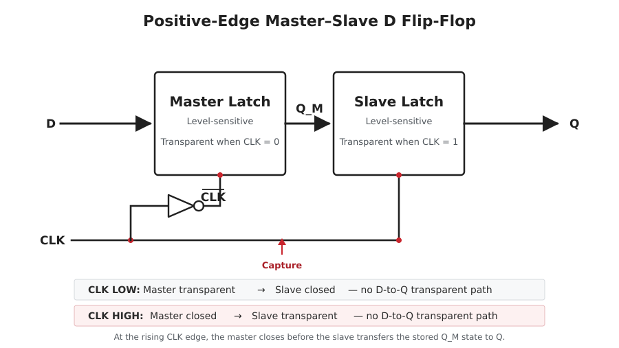
This model explains edge behavior, but a modern standard-cell or packaged flip-flop may use optimized internal circuits rather than a literal pair of textbook latch blocks. Its datasheet timing and function table remain the authoritative description of the external behavior.
Time Borrowing in Latch-Based Pipelines
A flip-flop pipeline assigns a largely fixed interval from one active clock edge to the next. If one combinational path exceeds that interval, unused slack in the following stage does not automatically rescue it. The slow stage fails setup unless the clock period, logic or pipeline partition changes.
A receiving latch remains open for part of its active phase. Data can arrive after the nominal phase boundary and still be captured before the latch closes. The extra interval is time borrowed from the following stage. It increases the budget of the late path while reducing the time available after that latch.
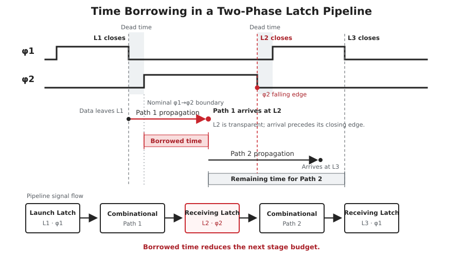
Borrowing does not create additional cycle time. Static timing analysis must account for clock phase, duty cycle, uncertainty, skew, minimum delay and the closing edge of every latch. The technique is useful in carefully controlled ASIC pipelines where the clock scheme and cell library are characterized for level-sensitive timing.
Race-Through and Clock-Phase Control
Two same-polarity latches connected in series can become transparent at the same time. If the combinational path between them is short enough, a new value may pass through both storage stages during one Enable phase. The intended one-stage-per-phase sequence is then lost.
Alternating positive- and negative-level latches, or two non-overlapping clock phases, prevent a continuous open path. Non-overlap needs verified margin across clock skew, process, voltage and temperature. Excessive dead time reduces the available data interval, while phase overlap reintroduces race-through risk.
Edge-triggered flip-flops simplify this aspect of system timing because each stage samples at a defined edge. They still require hold analysis. Fast data paths combined with clock skew can reach the next flip-flop too soon after its sampling edge, producing a minimum-delay failure.
74HC573 vs 74HC574: A Practical Device Comparison
The 74HC573 and 74HC574 both handle eight data bits and provide three-state outputs, but their storage controls are different. The 573 uses Latch Enable. The 574 uses a positive-edge clock.
| Feature | 74HC573 | 74HC574 | Selection impact |
|---|---|---|---|
| Storage type | Eight transparent D latches | Eight positive-edge D flip-flops | Choose level acceptance or edge sampling. |
| Capture control | LE HIGH: transparent; LE LOW: hold | Stores on the LOW-to-HIGH CP transition | The same control pulse can produce different output histories. |
| Data activity during control HIGH | Can propagate to Q while outputs are enabled | Ignored after the rising edge until the next edge | Glitches and multiple transitions are handled differently. |
| Output Enable | OE HIGH places outputs in high impedance | OE HIGH places outputs in high impedance | OE controls bus connection and does not replace LE or CP. |
| Typical use | Address holding, temporary bus transparency and I/O ports | Edge-aligned output registers and synchronous bus capture | Interface protocol timing determines the suitable device. |
The similar package role does not make the devices functionally interchangeable. A board designed around the 573 may depend on data passing throughout an LE window. Installing a 574 would capture only at the rising edge of that signal. The reverse substitution can allow unintended input activity to pass while the control remains HIGH.
Logic-family suffixes also matter. HC and HCT versions use different input-level specifications even when the functional number is the same. Verify supply range, input thresholds, output drive, propagation limits, package pinout and temperature grade for the complete ordering code.
ASIC, FPGA and Board-Level Use
ASIC Timing
Latch-based ASIC pipelines can improve timing flexibility through time borrowing and may use compact level-sensitive cells. The gain depends on the standard-cell library, clock distribution, test strategy and timing methodology. Scan insertion, phase generation and hold closure require deliberate support throughout the flow.
FPGA Logic
Modern FPGA fabrics are organized around abundant edge-triggered registers and tool flows optimized for synchronous edge-to-edge timing. Some device families provide latch-capable primitives, yet unintended latch inference remains a common RTL defect. Incomplete assignments in a combinational process can create storage that the designer never planned.
Board-Level Interfaces
Discrete latch ICs remain useful when a parallel bus must remain transparent during part of a control cycle or when an address must be held after multiplexed pins change function. Edge-triggered registers suit interfaces that define one sampling edge and require stable outputs for the rest of the cycle.
Latch and Flip-Flop HDL Coding
SystemVerilog separates intentional level-sensitive and edge-triggered storage with different procedural blocks. The latch omits an assignment while disabled so the previous state is retained. The flip-flop assigns on the specified clock edge.
// Intentional positive-level D latch
always_latch begin
    if (en)
        q_latch <= d;
end
// Positive-edge D flip-flop
always_ff @(posedge clk) begin
    q_ff <= d;
end
An incomplete assignment in an intended combinational block can infer a latch. For example, an if branch that assigns an output without a matching default or else requires the output to retain its previous value. Synthesis supplies storage to satisfy that behavior. Review inferred-latch warnings and use complete assignments whenever the process is meant to be combinational.
How to Choose Between a Latch and a Flip-Flop
- Choose a latch when the interface explicitly requires a transparent data window, the ASIC timing plan uses controlled time borrowing, or a bus must pass data during one phase and retain it during another.
- Choose a flip-flop when data must be aligned to a specified edge, the design uses a conventional synchronous FPGA flow, or fixed edge-to-edge timing is easier to verify.
- Check the source protocol: identify whether it guarantees a stable level across a window or a valid value around one edge.
- Check every capture boundary: apply setup and hold limits to the latch-closing edge or flip-flop sampling edge.
- Check minimum delay: prevent race-through in latch pipelines and hold failure in flip-flop pipelines.
- Check initialization: select reset or preset behavior when an unknown power-up state is unsafe.
- Check Output Enable separately: a three-state OE pin controls bus ownership; it does not define when internal data is captured.
- Check the implementation target: confirm that the ASIC library, FPGA architecture or board-level device supports the intended timing model.
Component selection should start from the required timing behavior rather than the family name printed in a schematic. Aetrix Electronics can support logic IC RFQs, ordering-code verification and sourcing review for transparent latches, flip-flops and registered bus devices.
Technical References
- Nexperia 74HC573/74HCT573 octal transparent latch product information
- Nexperia 74HC574/74HCT574 positive-edge octal flip-flop product information
- Nexperia 74HC74/74HCT74 dual positive-edge D flip-flop product information
- Intel Quartus Prime Pro Edition recommended design practices
- AMD LDCE transparent latch primitive documentation
Frequently Asked Questions
What is the main difference between a latch and a flip-flop?
A latch is level-sensitive, so its input can affect the output throughout an active Enable level. A flip-flop is edge-triggered and captures data around a specified clock transition. This changes the capture window, propagation paths, timing analysis and race conditions.
Is a D latch the same as a D flip-flop?
No. Both use a D input and store one bit, but a D latch is transparent during its active level. A D flip-flop samples D around its active edge and holds that result between edges.
Is a latch faster than a flip-flop?
A latch can present data before a clock edge and can support time borrowing, while a flip-flop adds clock-to-Q delay after its sampling edge. Overall speed depends on the cell implementation, clock phases, path delays, loading and timing constraints, so device type alone does not guarantee a faster system.
Can both latches and flip-flops become metastable?
Yes. A latch can violate setup or hold time near the edge that closes its transparent window. A flip-flop can violate the same requirements near its active clock edge. Either event can delay resolution or produce an unpredictable stored value.
What is time borrowing in a latch pipeline?
Time borrowing allows data to arrive after a nominal phase boundary while the receiving latch remains transparent. The data must still arrive before that latch closes. The borrowed interval reduces the timing available to the following stage.
Why can cascaded latches suffer race-through?
If two cascaded latches are transparent at the same time, a new value can pass through both stages during one control phase. Alternating latch polarities or verified non-overlapping clock phases prevent a continuous open path.
Why are flip-flops usually preferred in FPGA designs?
FPGA fabrics and timing tools are primarily optimized around abundant edge-triggered registers and synchronous clock networks. Intentional latches may be supported on some architectures, but they can reduce portability and complicate timing. Unexpected inferred latches should be corrected in the RTL.
What is the difference between the 74HC573 and 74HC574?
The 74HC573 is an octal transparent D latch: data passes while LE is HIGH and is stored when LE goes LOW. The 74HC574 is an octal positive-edge D flip-flop that captures data on the rising CP edge. Both provide three-state outputs.


