
 My Inquiry
 My Account


D Latch Circuit: Truth Table, Timing, ICs and Applications
Article Details
A D latch stores one bit under the control of an Enable input. In a positive-level D latch, Q follows D after the propagation delay while Enable is HIGH. When Enable goes LOW, the input path closes and Q retains the last valid D level. The circuit is level-sensitive: the complete active interval can pass data, rather than a single clock edge.
The D input also removes the ordinary forbidden command combination of a gated SR latch. Internal logic derives mutually exclusive Set and Reset conditions from D and its complement. The storage core therefore receives a request to store either 0 or 1 whenever the latch is enabled, while the disabled condition returns both control paths to Hold.
The broader relationship between SR, gated SR and D storage is covered in the latch circuit reference. A D-latch design review concentrates on transparency, the closing edge of Enable, setup and hold limits, multi-bit data capture, and the separate roles of Latch Enable and Output Enable.
Enable HIGH: the positive-level latch is transparent, so valid changes at D propagate to Q.
Enable LOW: Q holds the data captured when the transparent interval closed.
Timing boundary: D must satisfy the specified setup and hold times around the HIGH-to-LOW transition of Enable.
How a D Latch Removes the SR Forbidden Input
A gated active-HIGH SR latch can be converted into a D latch by driving its internal commands from one data input. The Set path is formed as S = EN · D. The Reset path is formed as R = EN · D̅. When EN = 1, D and D̅ guarantee that only one command is active. When EN = 0, S and R are both 0 and the SR core holds its previous state.
A NAND implementation uses active-LOW control signals instead. One input network produces S̅ and the other produces R̅. With Enable inactive, both become HIGH, which is the Hold condition for the cross-coupled NAND core. With Enable active, the two paths steer complementary commands into the core. The external behavior remains the same even though the internal command polarity is reversed.
The single D input prevents a normal data value from requesting Set and Reset simultaneously. It does not remove timing limits. If D changes too close to the closing transition of Enable, internal nodes can receive a marginally timed decision and the final stored value may be unpredictable for that event.
Positive-Level D Latch Circuit
A gate-level positive D latch contains an inverter, two gating paths and a bistable storage core. D drives the Set path directly and the Reset path through the inverter. Enable qualifies both paths. The cross-coupled gates then retain the selected value after Enable returns LOW.
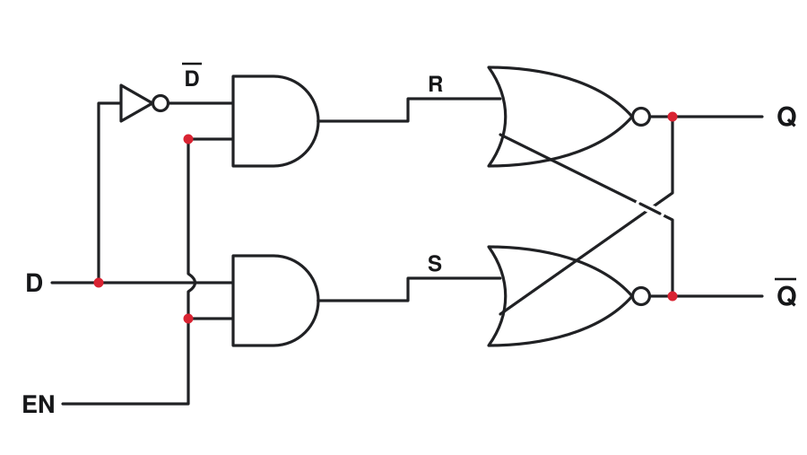
Integrated CMOS latches are often implemented with transmission gates and inverters rather than a literal collection of AND and NOR symbols. A transmission gate passes D to an internal storage node while the latch is open. When the control phase changes, the input switch opens and a feedback path closes around the storage inverters. The pin-level function is still described by the same D, Enable and Q behavior.
Some symbols label the control input G, C, CLK, Strobe or LE. The label alone does not establish edge-triggered operation. A datasheet function table that says the output follows D throughout one control level identifies a latch. A triangle on a logic symbol normally identifies an edge-triggered clock input.
D Latch Truth Table and Characteristic Equation
| Enable | D | Q(next) | Q̅(next) | Operating state | Meaning |
|---|---|---|---|---|---|
| 0 | X | Q(previous) | Q̅(previous) | Hold | Changes at D do not alter the stored state. |
| 1 | 0 | 0 | 1 | Transparent LOW | Q follows a valid LOW at D after propagation delay. |
| 1 | 1 | 1 | 0 | Transparent HIGH | Q follows a valid HIGH at D after propagation delay. |
The X in the Hold row means "do not care." It does not mean that D is electrically undefined or may be left floating. CMOS inputs still require a valid logic level or a defined bias. X only states that either a valid 0 or a valid 1 at D leaves Q unchanged while Enable is inactive.
For a positive-level latch, the ideal characteristic relation is:
The equation describes the logical state after the circuit has settled. It does not include propagation delay, minimum pulse width, supply ramp behavior, setup time, hold time or metastability. Those limits come from the implementation and must be taken from the exact device or timing library.
Transparent and Hold Intervals
Transparency lasts for the entire active Enable level. If D toggles three times while EN remains HIGH, Q can also toggle three times, each change shifted by the relevant D-to-Q propagation delay. The latch does not wait for EN to fall before updating Q.
When EN falls, the latch closes. The value retained at Q is the value presented at D with enough margin around that closing transition. Later changes at D have no effect until EN becomes active again. A negative-level D latch follows the same principle with the polarities reversed: it is transparent while Enable is LOW and closes when Enable rises.
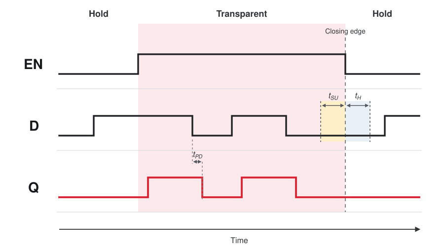
"Transparent" describes data transfer from D to Q. It does not mean that Q is disconnected or high impedance. A transparent latch normally drives a valid HIGH or LOW at Q. A separate Output Enable pin is required when the package must release a shared bus.
D Latch Video: Circuit, Operation and Truth Table
Video: "D Latch Explained: Basics, Working, Circuit, Case Study & Truth Table," Engineering Funda.
Timing Parameters That Decide Whether Data Is Stored Correctly
| Parameter | Measured relationship | Design consequence |
|---|---|---|
| Data setup time, tsu | Minimum time D must be stable before the latch-closing transition | Late-arriving data may store the old value, the new value or enter a metastable condition. |
| Data hold time, th | Minimum time D must remain stable after the closing transition | Changing D too early can disturb the value being isolated inside the latch. |
| D-to-Q propagation, tpd(D-Q) | Delay from a valid D transition to Q while the latch is transparent | Determines how quickly combinational changes can pass through an open latch. |
| Enable-to-Q propagation, tpd(EN-Q) | Delay from opening the latch to the corresponding Q response | Affects the beginning of the transparent window and downstream timing. |
| Minimum Enable pulse width | Shortest active or inactive interval accepted by the device | A narrow control pulse may fail to pass or retain data reliably. |
| Output-enable delay | Time from OE change to an actively driven or high-impedance output | Controls bus turn-on and turn-off; it does not describe internal data capture. |
Setup and hold are referenced to the edge that closes the latch. For a positive-level latch, that is the falling edge of Enable. The rising edge opens the path and is mainly associated with Enable-to-Q delay. Treating both edges as equivalent clock edges produces incorrect timing constraints.
A setup or hold violation does not guarantee that Q will visibly oscillate. The latch may resolve to 0 or 1, or Q may take longer than the specified propagation limit to reach a valid level. Digital simulation without timing checks can hide this behavior because an ideal model resolves events without analog regeneration.
D Latch vs D Flip-Flop
| Characteristic | D latch | D flip-flop |
|---|---|---|
| Sensitivity | Level-sensitive | Edge-triggered |
| When input can affect output | Throughout the active Enable level | Only around the specified rising or falling clock edge |
| Data movement | Multiple D transitions may pass while open | One value is sampled per active edge |
| Timing reference | Setup and hold around the latch-closing edge | Setup and hold around the active sampling edge |
| Timing flexibility | Supports time borrowing across an active phase | Uses a fixed edge-to-edge timing budget |
| Common design risk | Race-through if same-phase latches create an open path | Clock skew, setup/hold violations and clock-to-Q delay |
Time borrowing allows a slow combinational path to use part of the interval during which the receiving latch remains open. That flexibility is useful in latch-based ASIC timing, but the analysis must cover minimum and maximum delays, clock duty cycle, phase overlap, hold constraints and process variation.
Two positive-level latches placed in series on the same Enable signal can become transparent together. A change at the first input may race through both stages during one active interval. Two-phase systems avoid this with alternating latch polarities or non-overlapping phases. Board-level designs often use edge-triggered flip-flops when the additional timing discipline of latch pipelines offers no practical benefit.
Latch Enable and Output Enable Are Different Controls
Parallel latch ICs such as the 74HC373 and 74HC573 commonly provide both LE and OE. LE controls the internal storage operation. OE controls whether the output drivers are connected to the external pins. Mixing these functions can create bus contention or update data at the wrong time.
| Control | Typical active state | Internal latch | External Q pins |
|---|---|---|---|
| LE | HIGH | Transparent; D can update the stored state | Drive the corresponding state when outputs are enabled |
| LE | LOW | Holds the last valid input word | Continue driving the stored word when outputs are enabled |
| OE | LOW on common 74HC373/573 devices | No change to stored data | Output drivers enabled |
| OE | HIGH on common 74HC373/573 devices | Can retain old data or accept new data according to LE | High-impedance state |
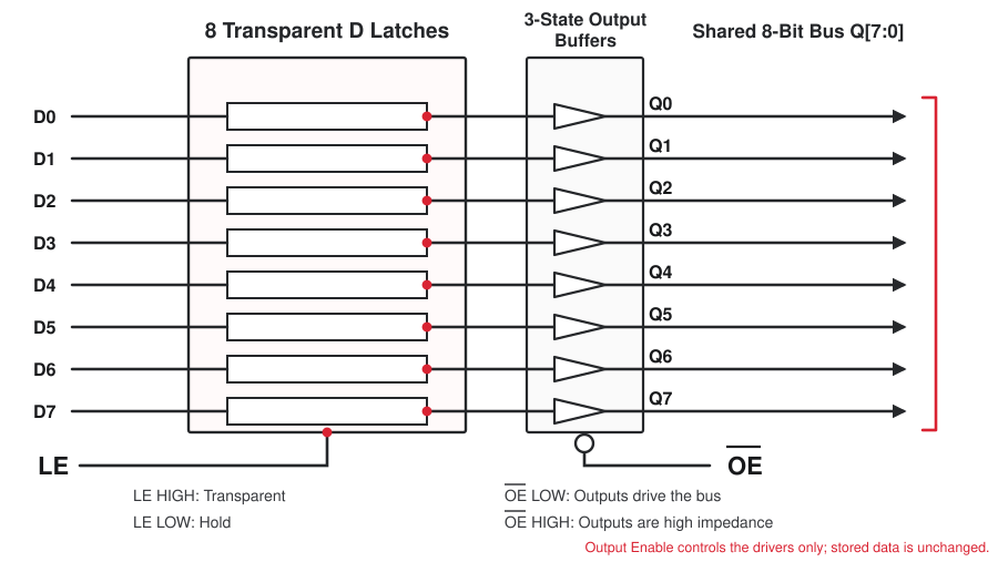
Bus control must include dead time when two devices can drive the same conductors. Taking one OE inactive and another active at the same nominal instant does not prove that their output drivers avoid overlap; compare the specified disable and enable delays. Pull resistors may establish an idle level, but they do not prevent contention between two active push-pull outputs.
Common D Latch ICs
| Device family | Configuration | Control behavior | Useful design context |
|---|---|---|---|
| 74HC373 | Eight transparent D latches with 3-state true outputs | LE HIGH is transparent; OE̅ LOW enables outputs | Buffer registers, I/O ports and parallel bus storage |
| 74HC573 / 74HCT573 | Eight transparent D latches with 3-state outputs | Same basic LE/OE function with a flow-through pin arrangement | PCB routing where D inputs and Q outputs should run in the same direction |
| CD4042B | Four clocked D latches with complementary outputs | Polarity input selects the transparent clock level | Wider-voltage CD4000-series control and holding-register functions |
| ASIC standard-cell latch | Single-bit level-sensitive storage, instantiated individually or as an array | Polarity, scan and reset options depend on the characterized cell | Time borrowing, integrated clock-gating cells and controlled sequential paths |
The ordering code still determines logic thresholds, supply range, output drive, package, temperature grade and automotive qualification. HC and HCT parts may share a functional number while using different input thresholds. A substitution review should therefore compare the complete datasheets rather than matching only the "373," "573" or "4042" family number.
Practical D Latch Applications
Address and Data Bus Holding
A multiplexed processor interface may place an address on shared pins during one phase and data on the same pins during another. A transparent latch accepts the address while LE is active, then holds it for the memory or peripheral after the processor changes the pins to data. The closing edge and bus skew must meet the latch setup and hold limits for every bit.
Parallel I/O Expansion
An octal latch can capture a control word and keep relays, indicators or logic-control lines stable while a controller reuses its data bus. Output current, simultaneous-switching noise and startup state still need separate checks. Loads above the logic device rating require suitable drivers rather than relying on the latch package to supply actuator current.
Glitch-Free Clock-Gating Control
Integrated clock-gating cells often use a latch to hold the enable command while the source clock is in its inactive phase. The stored enable cannot change during the clock phase in which a transition would create a shortened or extra pulse. Discrete gate-and-latch replacements require careful polarity and timing analysis; dedicated clock-gating cells include characterized behavior for this task.
Latch-Based Timing Pipelines
Alternating positive- and negative-level latches divide a cycle into controlled phases. A late signal can borrow time from the next phase while still meeting the following latch boundary. The method can improve performance and area in custom logic, but it increases the work required for hold analysis, duty-cycle control, test insertion and static timing closure.
D Latch Design Checks
- Confirm the active level: identify whether the latch is transparent HIGH or LOW from the function table, not from the signal name alone.
- Constrain the closing edge: verify D setup and hold time at the transition that ends transparency.
- Check the full data word: include bus skew so all bits belong to the intended transfer.
- Separate LE from OE: use LE for storage timing and OE for bus ownership.
- Avoid floating CMOS inputs: unused D, LE and OE pins need defined levels consistent with the device datasheet.
- Define startup behavior: assume stored data is unknown at power-up unless initialization is explicitly guaranteed.
- Prevent race-through: do not open cascaded same-phase latches across an unintended combinational path.
- Verify voltage compatibility: compare VIH, VIL, input clamp behavior, supply sequencing and output drive for the exact logic family.
- Place decoupling locally: connect the package supply to a nearby bypass capacitor and a low-inductance return path.
Testing and Troubleshooting a D Latch
Start with a slow pattern that separates the two modes. Hold Enable inactive and toggle D; Q should remain unchanged. Activate Enable and toggle D again; Q should follow after the propagation delay. Close the latch with D at 0, repeat with D at 1, and confirm that both values can be retained.
If Q always follows D, inspect the Enable level, pin mapping and solder connections before blaming the storage core. If Q never changes, check OE on three-state devices, the supply and ground pins, the D input level and the minimum Enable pulse width. A logic analyzer connected only to an external high-impedance bus can make a correctly stored internal state appear missing when OE is inactive.
Intermittent wrong words near the closing edge usually point to setup, hold or input-skew violations. Move the D transition away from the closing edge and repeat the test. A large improvement with added margin supports a timing diagnosis. Scope the actual device pins when ringing, slow edges or level translation may cause the input to cross logic thresholds later than the controller waveform suggests.
Component selection or production support for D-latch circuits should use complete ordering codes and verified timing data. Aetrix Electronics can assist with logic component RFQs, package verification and sourcing review for transparent latches, bus-storage devices and related logic families.
Technical References
- Texas Instruments SN54HC373/SN74HC373 Octal Transparent D-Type Latches datasheet
- Nexperia 74HC573/74HCT573 Octal D-Type Transparent Latch datasheet
- Texas Instruments CD4042B CMOS Quad Clocked D Latch datasheet
Frequently Asked Questions
What is a D latch?
A D latch is a level-sensitive one-bit storage circuit with Data and Enable inputs. In a positive-level device, Q follows D while Enable is HIGH. When Enable becomes LOW, Q retains the last D value that satisfied the required setup and hold times.
Why is a D latch called a transparent latch?
The latch is transparent during its active Enable level because valid changes at D can propagate through to Q. Transparency lasts for the complete active interval. It does not describe a high-impedance output; three-state control requires a separate Output Enable function.
What is the truth table of a positive-level D latch?
When Enable is LOW, D is ignored and Q holds its previous state. When Enable is HIGH and D is LOW, Q becomes LOW. When Enable is HIGH and D is HIGH, Q becomes HIGH. The output changes after the applicable propagation delay.
How does a D latch avoid the forbidden state of an SR latch?
Internal gating derives Set and Reset from D and its complement, so normal data operation cannot assert both commands together. With Enable inactive, both internal paths return to Hold. Timing violations near the closing edge can still make the captured value unpredictable.
What is the difference between a D latch and a D flip-flop?
A D latch is level-sensitive and can pass multiple input changes during its transparent phase. A D flip-flop samples D only around its active clock edge. Their setup, hold and propagation specifications must therefore be applied to different timing boundaries.
What happens if D changes near the closing edge of a latch?
If D violates setup or hold time, the latch may store the old value or the new value, or take longer than the specified delay to resolve. The design must keep D stable around the closing transition rather than assigning a guaranteed result to the violation.
Does Output Enable change the data stored in a 74HC373 or 74HC573?
No. Output Enable controls the external three-state drivers. The internal latches continue to retain or accept data according to Latch Enable. Taking OE inactive can disconnect Q from a bus without clearing the stored word.
Does a D latch power up with Q at zero?
A basic D latch should be treated as having an unknown startup state unless the exact device guarantees initialization. A system that requires a defined output must load known data under a qualified Enable condition or use a latch with a specified reset function.


