
 My Inquiry
 My Account


SR Latch Explained: NOR and NAND Circuits, Truth Tables, and Applications
Article Details
An SR latch is a one-bit bistable memory circuit controlled by Set and Reset inputs. A Set command makes Q HIGH, a Reset command makes Q LOW, and the cross-coupled feedback path keeps that state after the command is removed. The basic circuit has no clock and remains responsive to its control inputs whenever power is applied.
Two common implementations use cross-coupled NOR gates or cross-coupled NAND gates. Their stored function is similar, but their input polarities are opposite. A NOR SR latch normally has active-HIGH S and R inputs. A NAND SR latch normally uses active-LOW S̅ and R̅ inputs. Reading the gate symbols without checking the input polarity is a reliable way to reverse the Set, Reset and Hold conditions.
The wider relationship between SR, gated SR and D latches is covered in the latch circuit reference for SR and D latches. An SR-specific design review concentrates on feedback behavior, input polarity, forbidden-state recovery, timing limits and circuits that need independent Set and Reset controls.
NOR SR latch: S and R are active HIGH; S = 0 and R = 0 is the Hold condition.
NAND SR latch: S̅ and R̅ are active LOW; S̅ = 1 and R̅ = 1 is the Hold condition.
Design restriction: do not assert Set and Reset together unless the exact device or logic primitive explicitly defines which input has priority.
How Cross-Coupled Feedback Stores a Bit
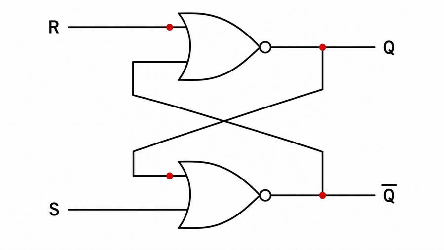
Each gate receives the output of the other gate. In a NOR implementation, Q can be written as the NOR of R and Q̅, while Q̅ is the NOR of S and Q. Once Q = 1 and Q̅ = 0, the LOW feedback into the Q-producing gate permits Q to remain HIGH. The HIGH level at Q simultaneously forces Q̅ LOW. The opposite state reinforces itself in the same way.
For valid active-HIGH input combinations, the characteristic relation is often written as Q(next) = S + Q(previous)R̅, with the restriction that S and R must not both equal 1. The restriction is part of the model. Extending that equation into the forbidden input condition silently introduces a priority rule that the simple two-NOR circuit does not provide.
Memory therefore comes from regeneration rather than a capacitor deliberately holding charge. A valid Set or Reset pulse starts a change, and propagation through the feedback loop completes it. The pulse must satisfy the minimum width and input-level requirements of the gates or latch IC; an ideal truth table cannot prove that a very narrow pulse will be captured.
NOR-Gate SR Latch: Active-HIGH Set and Reset
Two cross-coupled 2-input NOR gates form the standard active-HIGH SR latch. R connects to the gate producing Q, and S connects to the gate producing Q̅. This arrangement may look reversed at first: asserting R forces Q LOW directly, while asserting S forces Q̅ LOW and allows the feedback path to drive Q HIGH.
| S | R | Q(next) | Q̅(next) | State | Circuit behavior |
|---|---|---|---|---|---|
| 0 | 0 | Q(previous) | Q̅(previous) | Hold | Neither input overrides the feedback loop. |
| 1 | 0 | 1 | 0 | Set | S forces Q̅ LOW; feedback drives Q HIGH. |
| 0 | 1 | 0 | 1 | Reset | R forces Q LOW; feedback drives Q̅ HIGH. |
| 1 | 1 | 0 | 0 | Forbidden | Both outputs are forced LOW; the released state is not defined. |
The Hold row does not mean that Q must be LOW. It means that Q keeps whichever valid value was established earlier. A truth table that lists only the present inputs cannot replace the previous-state term because the same S = 0, R = 0 input can legitimately produce Q = 0 or Q = 1.
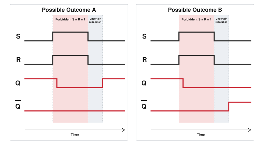
During the forbidden S = 1, R = 1 condition, both outputs become LOW and cease to be complementary. Returning both inputs LOW together releases both gates at nearly the same time. Gate-delay mismatch, routing skew, supply noise and temperature determine which internal node rises first. The next stored value is therefore not controlled by the logical inputs.
NAND-Gate SR Latch: Active-LOW Inputs
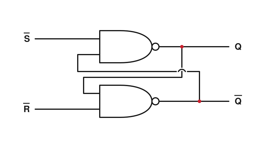
A NAND SR latch reverses the command polarity. The input names should be written S̅ and R̅, /S and /R, or with input bubbles on the logic symbol. Pulling S̅ LOW sets Q HIGH. Pulling R̅ LOW resets Q. Both inputs must be HIGH for the ordinary Hold state.
| S̅ | R̅ | Q(next) | Q̅(next) | State | Circuit behavior |
|---|---|---|---|---|---|
| 1 | 1 | Q(previous) | Q̅(previous) | Hold | Neither active-LOW command is asserted. |
| 0 | 1 | 1 | 0 | Set | S̅ LOW forces Q HIGH. |
| 1 | 0 | 0 | 1 | Reset | R̅ LOW forces Q LOW. |
| 0 | 0 | 1 | 1 | Forbidden | Both outputs are forced HIGH; the released state is not defined. |
Active-LOW inputs are common in reset networks, alarm lines and wired control systems, but the overbar must follow the signal through the complete schematic. Relabelling S̅ as S without also inverting the truth table changes the circuit function. Pull resistors should establish the inactive HIGH level before the driving source becomes valid.
Dedicated latch ICs may document a set-dominant or reset-dominant result when both inputs are asserted. That documented priority belongs to the exact device implementation. It should not be transferred to a two-NAND gate latch or to a different manufacturer's part solely because both devices carry an SR or 74x279 description.
SR Latch Video: NOR, NAND and Gated Operation
Video: "SR Latch and Gated SR Latch Explained," ALL ABOUT ELECTRONICS.
NOR vs NAND SR Latch
| Characteristic | NOR SR latch | NAND SR latch |
|---|---|---|
| Command polarity | Active HIGH | Active LOW |
| Hold inputs | S = 0, R = 0 | S̅ = 1, R̅ = 1 |
| Set command | S = 1, R = 0 | S̅ = 0, R̅ = 1 |
| Reset command | S = 0, R = 1 | S̅ = 1, R̅ = 0 |
| Forbidden inputs | S = 1, R = 1 | S̅ = 0, R̅ = 0 |
| Outputs while forbidden | Q = 0 and Q̅ = 0 | Q = 1 and Q̅ = 1 |
| Common discrete gate family | 74HC02, 74LVC02 or equivalent NOR gates | 74HC00, 74LVC00 or equivalent NAND gates |
The correct implementation is usually the one that matches the polarity already present in the system. An active-LOW fault line can drive a NAND-based latch without an added inverter. An active-HIGH comparator output fits a NOR-based latch. Logic voltage, input thresholds, pulse width, power-up behavior and package availability still have to be checked for the selected family.
What Happens in the Forbidden State
The forbidden state creates two separate problems. First, Q and Q̅ are driven to the same logic level while both commands are active. Any downstream circuit that assumes complementary outputs can respond incorrectly. Second, removing the two commands together creates a race around the feedback loop. The latch may resolve to Set, resolve to Reset, or spend longer than the normal propagation delay in an intermediate analog state.
Metastability and logical unpredictability are related but not identical. The logic table cannot predict the final state after simultaneous release, even if the latch resolves quickly. Metastability describes the physical condition in which internal nodes remain near a switching threshold for an abnormally long time. A downstream digital input can then see excessive delay or an uncertain logic level.
Reliable designs prevent the condition instead of assigning it an arbitrary truth-table value. Suitable methods include mutually exclusive source logic, a set-dominant or reset-dominant priority network, qualified input timing, or conversion to a D latch when only one data decision is required. If Q crosses into a synchronous clock domain, the receiving logic still needs an appropriate synchronizer.
Gated SR Latch and Explicit Priority
A gated SR latch adds an Enable input before the storage core. With Enable inactive, changes at S and R do not reach the latch. With Enable active, the circuit follows the ordinary Set, Reset and Hold behavior. Enable limits when commands are accepted; it does not make the simultaneous Set and Reset combination safe.
| Enable | S | R | Q(next) | Operation for an active-HIGH gated SR latch |
|---|---|---|---|---|
| 0 | X | X | Q(previous) | Input commands blocked |
| 1 | 0 | 0 | Q(previous) | Hold |
| 1 | 1 | 0 | 1 | Set |
| 1 | 0 | 1 | 0 | Reset |
| 1 | 1 | 1 | Undefined after release | Forbidden |
Priority must be stated when both commands are allowed. A reset-dominant latch guarantees Q = 0 when Set and Reset coincide; a set-dominant latch guarantees Q = 1. Microcontroller and programmable-logic peripherals may expose this choice explicitly. For example, Microchip's PWM fault-acceptance logic documents set-dominant and reset-dominant SR modes for different fault-handling requirements. A bare cross-coupled gate circuit has no equivalent priority guarantee.
Practical SR Latch Applications
SPDT Switch Debouncing
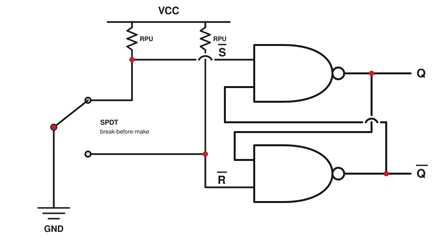
A changeover switch can generate mutually exclusive Set and Reset commands. In an active-HIGH NOR circuit, pull-down resistors hold both inputs LOW while the moving contact is between positions, and the selected contact connects one input HIGH. Bounce alternates that input between its command level and Hold; it does not request the opposite state, so Q changes once.
The active-LOW NAND version uses pull-up resistors and connects the selected input to ground. The switch should be break-before-make so both active commands are not created during travel. This method needs an SPDT contact. A single SPST pushbutton requires different conditioning because it does not naturally supply separate Set and Reset signals.
Fault and Alarm Capture
A comparator, tamper loop or protection circuit can assert Set when a fault appears. Q remains active after a short fault pulse disappears, giving a controller time to read the event. Reset comes from an acknowledgement or recovery signal. A safety-oriented design normally prevents Reset from clearing Q while the fault source remains active; this is where an explicit Set-dominant function can be useful.
Texas Instruments demonstrates the pattern in its alarm and tamper circuit using an S-R latch. When the latched output enters clocked logic, synchronize Q at the receiving boundary. The latch preserves the event, while the synchronizer controls metastability risk in the synchronous domain.
Short-Pulse and Event Memory
An event pulse may be too brief for firmware polling but still wide enough to meet the latch input specification. Set stores the event until a later Reset clears it. Typical uses include overflow flags, threshold crossings and test status signals. The latch is not a universal pulse catcher: pulses below the guaranteed minimum width or outside the valid input range can be missed.
Power and Control Interlocking
Independent commands can hold an enable, inhibit or shutdown state after a momentary request. The chosen priority must match the safe condition. If Reset releases power and Set forces shutdown, a safety-related design normally gives shutdown precedence and adds a defined power-on state. Software should not be the only element preventing simultaneous commands when the hardware controls an energetic load.
SR Latch ICs and Gate-Level Implementations
| Device or method | SR function | Design detail to verify | Suitable use |
|---|---|---|---|
| CD4043B | Four independent NOR R/S latches with a common 3-state output enable | Active-HIGH S and R; ENABLE controls the outputs, not the stored states | Multi-bit event storage and shared-bus control |
| CD4044B | Four independent NAND R/S latches with a common 3-state output enable | Active-LOW control convention and the exact function table | Negative-logic control and alarm storage |
| SN74LS279A family | Four active-LOW S-R latches; two sections include dual Set inputs | Legacy TTL supply and input levels, simultaneous-input behavior and lifecycle status | Maintenance of established TTL control boards |
| Two NOR gates | One active-HIGH SR latch | Use gates from the same compatible logic family and prevent floating inputs | Simple discrete control and laboratory circuits |
| Two NAND gates | One active-LOW SR latch | Inactive inputs require defined HIGH levels; verify minimum command pulse width | Active-LOW fault and reset networks |
| MCU configurable logic | SR function implemented in internal LUT and sequential logic resources | Input polarity, digital filtering, clock-domain boundary and startup configuration | Event capture without continuous CPU service |
Aetrix lists logic devices that can implement the gate-level forms, including the 74LVC1G02SE-7 single 2-input NOR gate and the 74HC00S14-13 quad 2-input NAND gate. Two single-gate NOR packages are required for one discrete NOR latch, while one quad NAND package provides enough gates for two independent basic NAND latches. The exact datasheet remains the authority for input type, supply range, propagation delay and unused-input handling.
For broader logic sourcing, the Nexperia product portfolio at Aetrix includes gates, latches and related logic families. Manufacturer, logic family, voltage range, package suffix and lifecycle status should be checked at the complete ordering-code level.
SR Latch Design Checklist
- Mark active levels: show overbars, bubbles or /S and /R notation consistently from the source to the latch pins.
- Define simultaneous-command behavior: prevent it, or select a device with a documented Set or Reset priority.
- Check voltage compatibility: compare guaranteed VIH and VIL levels, not only nominal supply voltages.
- Check timing limits: include minimum Set/Reset pulse width, propagation delay and input transition requirements over voltage and temperature.
- Initialize the state: provide a qualified power-on Set or Reset when an unknown Q can create a false alarm or unsafe enable.
- Control asynchronous boundaries: preserve short events with the latch, then synchronize Q before synchronous logic uses it.
- Do not leave CMOS inputs floating: use pull resistors or direct logic drive for every used and unused input.
- Decouple the IC: place the manufacturer-recommended bypass capacitor close to the supply pins and keep feedback routing short.
- Review output behavior: complementary outputs, Q-only outputs and 3-state outputs are not interchangeable.
Testing and Troubleshooting an SR Latch
Start with defined inactive input levels and a known initialization command. Apply Set, return to Hold, apply Reset, and return to Hold while observing S, R, Q and Q̅ on a logic analyzer or oscilloscope. Q should remain stable during each Hold interval. Measure the output transition from the input threshold crossing rather than from the instant a mechanical switch begins to move.
| Observed problem | Likely cause | Measurement or correction |
|---|---|---|
| Q changes without a command | Floating input, slow noisy edge or supply disturbance | Probe input levels, add defined biasing, verify input hysteresis and improve decoupling. |
| Set and Reset appear reversed | Active-LOW NAND latch interpreted as active HIGH | Check signal bars, input bubbles and the exact function table. |
| Power-up state changes between tests | No specified initialization path | Add power-on Set or Reset and verify its pulse width across supply ramp conditions. |
| Output is inconsistent after both commands | Release from the forbidden state | Prevent overlap or add explicit priority logic; do not tune trace delay to choose a winner. |
| Short event is occasionally missed | Pulse below minimum width or threshold, or excessive input filtering | Measure pulse amplitude and width at the latch pin under worst-case conditions. |
| Controller occasionally reads the wrong state | Asynchronous Q sampled without synchronization | Use a suitable synchronizer and design a safe reset handshake. |
SR Latch vs RS Latch Naming
SR latch and RS latch often refer to the same Set-Reset storage function. In basic gate diagrams, the order of the letters may only reflect naming convention. In HDL libraries, configurable logic peripherals and safety control blocks, the order can identify which command has priority when both are asserted. The symbol name alone is therefore insufficient; the simultaneous-input row of the function table decides the behavior.
Component selection or production support for SR latch circuits should use complete ordering codes and verified datasheets. Aetrix Electronics can assist with logic component RFQs, package verification and sourcing review for gates, latches and related control logic.
Technical References
- Texas Instruments CD4043B/CD4044B CMOS Quad 3-State R/S Latches datasheet
- Texas Instruments SN74LS279A Quadruple S-R Latches datasheet
- Analog Devices: R-S latch switch debouncing and real-world switch interfaces
- Microchip: implementing an SR latch with Configurable Custom Logic
Frequently Asked Questions
What is an SR latch?
An SR latch is a bistable logic circuit that stores one binary state through cross-coupled feedback. Set drives Q to 1, Reset drives Q to 0, and the Hold input combination preserves the previous value. The basic form responds asynchronously and does not need a clock.
How does an SR latch retain data after Set or Reset is removed?
Each gate output feeds an input of the opposite gate. Once a valid Q and Q̅ state is established, those feedback levels reinforce one another. Removing the Set or Reset command returns the inputs to Hold, allowing the feedback loop to maintain the bit while power remains applied.
What is the difference between a NOR and NAND SR latch?
A NOR SR latch normally uses active-HIGH commands and holds when S and R are both LOW. A NAND SR latch uses active-LOW commands and holds when S̅ and R̅ are both HIGH. Their forbidden combinations and output levels during those combinations are opposite.
Why is the simultaneous Set and Reset condition forbidden?
Simultaneous commands force Q and Q̅ to the same level, breaking their complementary relationship. Releasing both commands together also starts a feedback race. The final state depends on physical delay and skew and may pass through metastability, so ordinary logic equations cannot guarantee the result.
Does an SR latch need a clock signal?
A basic SR latch does not use a clock and responds whenever Set or Reset becomes active. A gated SR latch adds a level-sensitive Enable input that controls when commands can reach the storage core. It should not be confused with an edge-triggered SR flip-flop.
Can an SR latch debounce any pushbutton?
The classic SR debounce circuit works naturally with an SPDT changeover switch because its two contacts create separate, mutually exclusive Set and Reset commands. A single SPST pushbutton does not provide both commands and requires additional gates, RC conditioning, a Schmitt-trigger input or a dedicated debounce device.
Does an SR latch power up in a known state?
A basic cross-coupled latch has no guaranteed initial state unless the device or surrounding circuit specifies initialization. Small internal differences may make one state appear common during testing, but a reliable system uses a qualified power-on Set or Reset pulse when the initial output matters.
How should an asynchronous SR latch output connect to clocked logic?
The latch can preserve a short asynchronous event, but Q remains asynchronous to the receiving clock. Pass Q through an appropriate synchronizer before synchronous logic uses it, and design the Reset handshake so the stored event is not cleared before the receiving domain has safely observed it.


