
 My Inquiry
 My Account


Latch Circuit: SR and D Latches, Truth Tables, Timing, and Applications
Article Details
A latch circuit is a bistable digital storage element. It has two stable output states and can retain one binary value after the input that created that state is removed. In the static gate-based latches discussed here, storage comes from feedback: part of the output is returned to the input of the logic network, allowing the circuit to reinforce its present state.
This feedback separates a latch from a combinational gate. The output of an AND, OR or inverter is determined only by its present inputs. A latch output depends on the present inputs and the state established by earlier inputs. Remove power, however, and the stored bit is lost. Standard logic latches are volatile devices.
SR latches expose the feedback mechanism directly through Set and Reset inputs. D latches add input gating so that a single data input can be accepted during an enable window and held when that window closes. Multi-bit devices such as the 74HC373 and 74HC573 place several D latches in one package for bus buffering, I/O ports and working registers.
Latch circuit definition: a bistable logic circuit that stores one bit. A gated latch accepts data during an active control level and holds it when that control is inactive.
Do not confuse it with CMOS latch-up: latch-up is an unwanted parasitic current path inside a CMOS device, not a logic storage function.
How a Latch Circuit Stores One Bit
The simplest latch schematic uses two inverting logic stages connected in a loop. In an SR latch, these stages are normally two cross-coupled NOR gates or two cross-coupled NAND gates. Each gate receives an external control input and the output of the other gate. The outputs are labelled Q and Q̄, or Q and /Q.
Assume Q is HIGH and Q̄ is LOW. The LOW feedback presented to the gate producing Q allows Q to remain HIGH. Q then feeds a HIGH level into the opposite gate, forcing Q̄ to remain LOW. The two outputs reinforce one another. A valid Set or Reset input temporarily overrides this loop and moves it to the opposite stable state.
The change is not instantaneous. Each gate has propagation delay, so the new state travels around the feedback loop before settling. Logic diagrams often draw Q and Q̄ as exact complements, but that relationship can fail briefly during switching and permanently while a forbidden SR input combination is asserted.
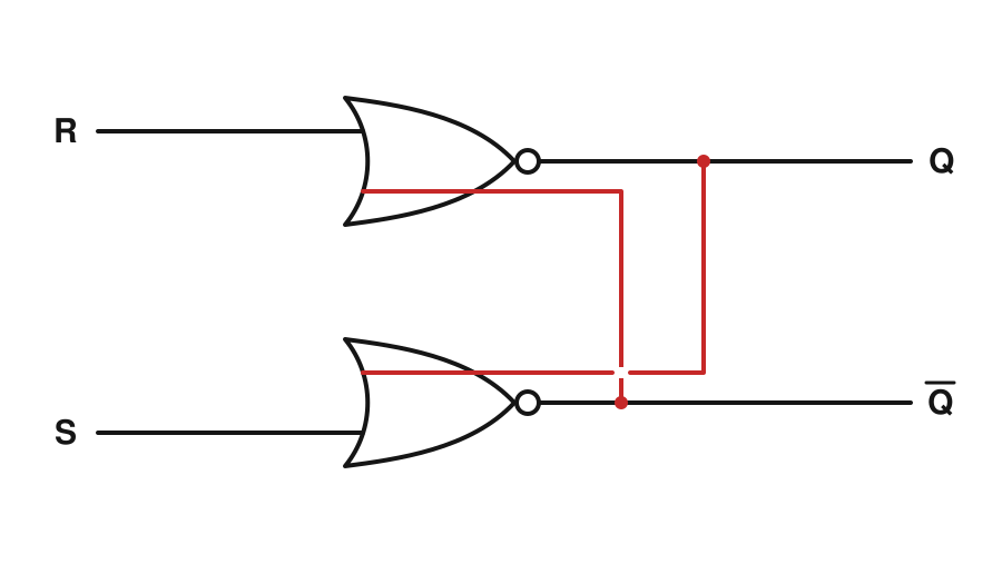
SR Latch Circuit Using NOR Gates
A NOR-gate SR latch uses active-HIGH Set and Reset inputs. Driving S HIGH sets Q to 1. Driving R HIGH resets Q to 0. With S and R both LOW, neither input requests a change and the feedback loop preserves the previous value.
| S | R | Q(next) | Q̄(next) | Operation |
|---|---|---|---|---|
| 0 | 0 | Q(previous) | Q̄(previous) | Hold the stored state |
| 1 | 0 | 1 | 0 | Set |
| 0 | 1 | 0 | 1 | Reset |
| 1 | 1 | 0 | 0 | Forbidden input combination |
The final row is forbidden because both NOR outputs are forced LOW, so Q and Q̄ stop being complementary. A second problem appears when S and R return LOW at nearly the same time. Small gate-delay differences determine which side wins the feedback race. The resulting state is not safely predictable from the ideal truth table.
An SR latch should therefore receive mutually exclusive Set and Reset commands. If the source logic can assert both, add priority logic, input interlocking or a defined recovery path rather than relying on matched gate delays.
NAND-Gate SR Latch and Active-LOW Inputs
Replacing the NOR gates with NAND gates reverses the active level of the control inputs. The inputs are commonly written S̄ and R̄ to show that a LOW level performs the action. S̄ = 0 sets Q, R̄ = 0 resets Q, and the latch holds its state when both inputs are HIGH.
| S̄ | R̄ | Q(next) | Q̄(next) | Operation |
|---|---|---|---|---|
| 1 | 1 | Q(previous) | Q̄(previous) | Hold the stored state |
| 0 | 1 | 1 | 0 | Set |
| 1 | 0 | 0 | 1 | Reset |
| 0 | 0 | 1 | 1 | Forbidden input combination |
The difference between NOR and NAND implementations is easy to miss on a schematic copied between positive-logic and negative-logic systems. Check the input bubbles, signal names and truth table together. An overbar in the signal name is part of the function, not a cosmetic notation.
SR Latch Circuit Video Walkthrough
The video follows both feedback paths through the Set, Reset and Hold conditions, including the way each output becomes an input to the opposite gate.
Video: "SR Latch Circuit – Basic Introduction," The Organic Chemistry Tutor.
Gated SR Latch
A basic SR latch responds whenever Set or Reset becomes active. A gated SR latch adds an Enable input ahead of the cross-coupled gates. When Enable is inactive, changes at S and R are blocked and the stored state remains unchanged. When Enable is active, S and R control the latch.
| Enable | S | R | Q(next) | Meaning |
|---|---|---|---|---|
| 0 | X | X | Q(previous) | Inputs blocked; hold |
| 1 | 0 | 0 | Q(previous) | Hold |
| 1 | 1 | 0 | 1 | Set |
| 1 | 0 | 1 | 0 | Reset |
| 1 | 1 | 1 | Undefined after release | Forbidden for a NOR-based gated latch |
Enable controls when the latch may change; it does not remove the forbidden SR combination. Deriving Set and Reset from D and its complement prevents both commands from becoming active during normal operation, producing a D latch.
D Latch Circuit: Data Storage with One Input
A D latch has a Data input and a level-sensitive Enable input. Internally, D drives one side of a gated SR structure and an inverted copy of D drives the other. The complementary input paths prevent the Set and Reset commands from being asserted together during normal operation.
For a positive-level D latch, Q follows D while Enable is HIGH. This interval is the transparent phase. When Enable goes LOW, the input path closes and Q retains the last valid D level. The circuit stores the value that satisfied the specified setup and hold times around the closing transition of Enable.
| Enable | D | Q(next) | Operating condition |
|---|---|---|---|
| 0 | X | Q(previous) | Latched; input changes are ignored |
| 1 | 0 | 0 | Transparent |
| 1 | 1 | 1 | Transparent |
"Transparent" does not mean high impedance. It means that a valid change at D can propagate through the latch to Q while Enable is active. Output Enable, when provided on an IC such as the 74HC373, is a separate function. OE can place the external output in a high-impedance state without clearing or freezing the internal latch.
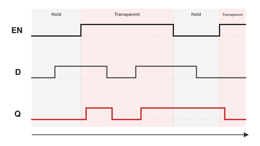
Types of Latches in Digital Electronics
Latch names describe the input function, the control method or the number of stored bits. The term should also state the active level when it affects interpretation. "SR latch" alone is incomplete if the reader cannot see whether Set and Reset are active HIGH or active LOW.
| Latch type | Inputs | Control behavior | Typical use |
|---|---|---|---|
| SR latch | Set, Reset | Asynchronous response to active input | Fault flags, event memory, control interlocking |
| Gated SR latch | Set, Reset, Enable | Accepts S and R only during the enable level | Enable-qualified control logic and temporary state storage |
| D latch | Data, Enable | Transparent during the active enable level; holds otherwise | Temporary data storage and timing pipelines |
| Addressable latch | Data, address, write control | Updates one selected output while other bits retain state | Control-output expansion |
| Multi-bit transparent latch | Parallel data, common LE, optional OE | Several D latches controlled together | Bus buffering, I/O ports and working registers |
JK and T functions can be implemented with level-sensitive storage, but many devices carrying those names are edge-triggered flip-flops. The function name alone does not establish whether a device is a latch. Check the function table and timing diagram for level-sensitive or edge-triggered behavior.
Latch vs Flip-Flop
The controlling event is the practical difference between a latch and a flip-flop. A latch is level-sensitive: input data may pass to the output for the full time that Enable is active. A flip-flop is edge-triggered: it samples data around a specified rising or falling clock edge and holds that value until the next active edge.
| Characteristic | Latch | Flip-flop |
|---|---|---|
| Input sensitivity | Active control level | Active clock edge |
| Data acceptance | Throughout the transparent window | Within setup and hold limits around one edge |
| Output activity | May follow multiple input changes while open | Normally changes once per active edge |
| Timing opportunity | Allows time borrowing across stage boundaries | Uses fixed edge-to-edge timing boundaries |
| Timing risk | Glitches can pass during transparency; race analysis is required | Clock skew, setup, hold and metastability remain critical |
| Common discrete example | 74HC373 or 74HC573 | 74HC374 or 74HC574 |
A master-slave flip-flop can be constructed from two latches driven by opposite clock phases. One latch accepts data while the other blocks it; their roles reverse when the clock changes phase. The pair behaves as an edge-triggered storage element even though each internal stage is level-sensitive.
Replacing a latch with a flip-flop is therefore not a pin-level timing substitution. The receiving logic sees a different data-valid window, and a design that relied on time borrowing through an open latch may fail after the change. Moving in the other direction can expose downstream logic to glitches that were previously blocked between clock edges.
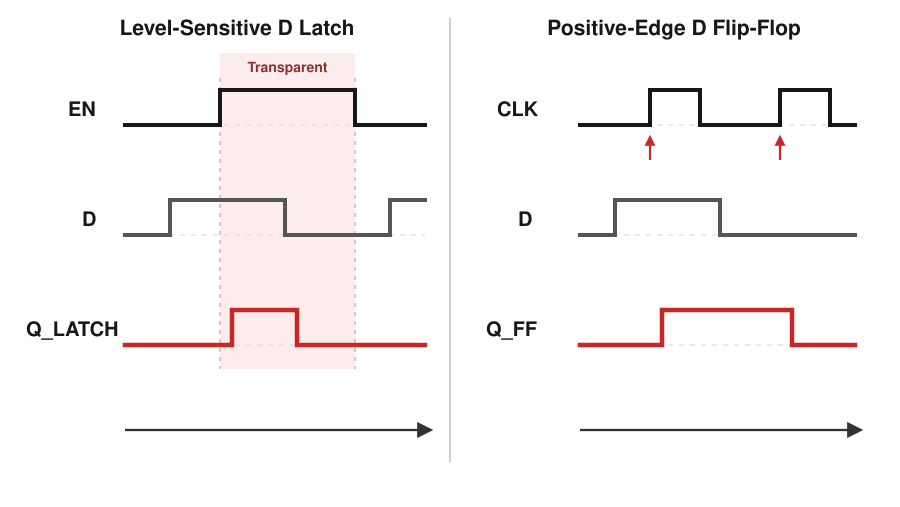
Latch Timing Parameters That Affect a Real Circuit
A correct truth table does not guarantee a reliable board or IC design. Supply voltage, temperature, load capacitance, input slew rate and logic family change the timing margin. Use the limits for the exact device and operating condition rather than a typical propagation number copied from another member of the family.
| Parameter | What it specifies | Design consequence |
|---|---|---|
| Propagation delay, tpd | Time from a valid D, LE, Set or Reset transition to the corresponding output change | Sets the earliest and latest response seen by downstream logic |
| Setup time, tsu | Minimum time data must be stable before the latch closes | Data arriving too late may be captured incorrectly or cause metastability |
| Hold time, th | Minimum time data must remain stable after the closing transition | Fast upstream changes can corrupt the stored value |
| Enable pulse width | Minimum duration of the active or inactive LE level | A narrow pulse may not open or close every internal channel correctly |
| Output-enable delay | Time required to enter or leave the high-impedance state | Controls bus handoff and the risk of two drivers overlapping |
Transparency, Glitches and Race-Through
While a D latch is transparent, an input glitch that meets the device thresholds and pulse-width requirements can reach Q. If several same-polarity latch stages are open at once, data may propagate through more than one stage during a single enable phase. Two-phase latch systems prevent this by arranging non-overlapping transparent windows and verifying minimum as well as maximum delays.
Setup, Hold and Metastability
If D changes too close to the closing transition of Enable, the feedback nodes can momentarily balance between logic states. The output may take longer than the normal propagation delay to resolve and may settle to either value. No logic family eliminates metastability; adequate timing margin and appropriate synchronizer structures reduce the probability that it reaches functional logic.
Power-Up State
A latch without an explicit reset should not be assumed to power up at 0 or 1. Internal mismatch may make one state more common on a bench sample, but that preference is not a reset specification. If system safety depends on the initial output, use a device with defined clear or preset behavior, or add a qualified power-on reset circuit.
Practical Latch Circuit Applications
Capturing a Fault or Short Event
A short alarm pulse can disappear before firmware polls a status pin. An SR latch converts the pulse into a persistent flag: the event asserts Set, Q remains active after the pulse ends, and a separate acknowledgement resets the flag. The reset path must be defined so that an active fault cannot be silently cleared and immediately hidden. Texas Instruments demonstrates this arrangement in an alarm and tamper circuit using an SR latch.
Mechanical Switch Debouncing
An SR latch can debounce a changeover switch when the two contacts generate mutually exclusive Set and Reset signals. Contact bounce on the newly selected side repeatedly requests the same final state instead of producing multiple output transitions. A single-pole pushbutton does not automatically provide complementary commands; it needs additional conditioning or a different debounce topology.
Bus Buffering and I/O Expansion
An octal transparent latch can capture eight parallel data bits and present them through 3-state outputs. This is useful when an address or data bus is shared, when a microcontroller must hold output values after a write cycle, or when external loads should be disconnected without erasing the stored byte. Bus contention analysis must include the output-enable turn-on and turn-off delays.
Clock Gating and Time Borrowing
Integrated clock-gating cells commonly use a latch to hold an enable signal stable during the active clock phase, preventing a mid-cycle enable transition from creating a shortened clock pulse. Latch-based pipelines can also let a slow logic path borrow time from the next stage. Both techniques depend on controlled clock phases and static timing analysis; they are not equivalent to inserting an arbitrary discrete latch on a PCB clock line.
Common Latch ICs and What Their Control Pins Do
| Logic family or device | Storage function | Important control detail | Typical design role |
|---|---|---|---|
| 74HC75 | Four transparent D latches with complementary outputs | Two active-HIGH latch-enable inputs, each controlling a pair of latches | Small parallel storage blocks requiring Q and Q̄ |
| 74HC373 / 74HCT373 | Eight transparent D latches with 3-state outputs | LE controls storage; OE controls only the external output state | Bus registers, I/O ports and parallel data holding |
| 74HC573 / 74HCT573 | Functionally similar octal transparent D latch | Flow-through or bus-structured pin arrangement places data and output pins on opposite sides | PCB layouts with straight bus routing |
| SN74LVC1G373 | Single D-type latch with 3-state output | LE may update the stored state while OE keeps Q in high impedance | One-bit buffering, I/O ports and working registers |
| CD4043B / CD4044B | Four independent 3-state SR latches | CD4043B uses NOR latches; CD4044B uses NAND latches | Independent event flags, strobed registers and general control logic |
Part-family names do not guarantee identical electrical limits across manufacturers or logic technologies. Confirm supply range, input thresholds, output drive, propagation delay, setup and hold time, OE behavior, package pinout and power-off protection for the exact ordering code.
Latch Circuit Design Checks
- Identify every active-LOW signal explicitly. A NAND SR latch and a NOR SR latch use opposite hold and command levels.
- Prevent the forbidden Set/Reset combination in hardware when both commands can originate asynchronously.
- Do not use OE as a substitute for LE. OE disconnects a 3-state output; it does not necessarily stop the internal latch from accepting data.
- Tie unused CMOS inputs to defined logic levels. Floating inputs can switch, increase supply current and disturb stored control states.
- Check setup, hold, propagation and enable-pulse limits over the full voltage and temperature range.
- Provide a defined initialization path when an unknown power-up state could energize a load, release a reset or report a false status.
- For shared buses, verify output-disable and output-enable timing so two devices cannot drive opposite levels simultaneously.
Frequently Asked Questions
What does a latch circuit store?
A basic latch stores one binary state. Q remains at 0 or 1 after the input command is removed because cross-coupled feedback reinforces the selected state. The value is volatile and disappears when power is removed unless another part of the system restores it.
Why does an SR latch have Q and Q̄ outputs?
The two cross-coupled gates naturally produce two opposing internal nodes. Under valid steady-state inputs, Q̄ is the complement of Q. During propagation and under the forbidden input combination, the outputs may briefly or continuously fail to be complementary.
What is the difference between NOR and NAND SR latch circuits?
A NOR SR latch normally uses active-HIGH Set and Reset inputs and holds when both inputs are LOW. A NAND SR latch uses active-LOW inputs and holds when both are HIGH. Their forbidden input combinations are also opposite.
Why is a D latch called transparent?
A positive-level D latch is transparent while Enable is HIGH because valid changes at D can propagate to Q during that interval. When Enable goes LOW, the path closes and the last valid data level is retained.
What is the main difference between a latch and a flip-flop?
A latch accepts data throughout an active enable level. A flip-flop samples data around a rising or falling clock edge. This difference changes the data-valid window, race conditions, timing analysis and the possibility of borrowing time between stages.
Does Output Enable clear a D latch?
Not on common 3-state devices such as the 74HC373. OE controls whether the stored value is driven onto the output pin. The internal latch can retain old data or accept new data according to LE while the output remains high impedance.
Does a latch power up in a known state?
Only when the device or surrounding circuit provides a specified initialization function. A plain feedback latch without reset should be treated as unknown after power-up, even if repeated tests on one sample appear to favor a particular state.
Can an SR latch debounce a mechanical switch?
Yes, particularly with a changeover switch that provides mutually exclusive Set and Reset contacts. Bounce then repeats the same command instead of producing repeated output changes. A single-contact pushbutton requires additional input conditioning or another debounce circuit.


