
 My Inquiry
 My Account


How to Test Dynamic Load Response in Low-Voltage High-Current Buck Converters
Article Details
Dynamic load response testing verifies whether a low-voltage high-current buck converter can keep the output rail within its allowed voltage window during fast load changes. For ASIC, FPGA, processor, switch-chip, and accelerator core rails, a static load test is not enough. A rail that is stable at hundreds of amperes can still produce excessive undershoot, overshoot, ringing, or recovery delay when the load current changes in nanoseconds or microseconds.
Low-voltage Vcore rails are especially sensitive because the output voltage may be near 0.8 V to 1.0 V, while the current can reach hundreds of amperes. A transient deviation of only a few tens of millivolts can be meaningful. The test method must capture the current step, voltage droop, overshoot, recovery time, probe location, remote sense behavior, capacitor network response, and control-loop recovery.
For system-level context, see High-Current ASIC Core Power Supply Design. For capacitor-network design, see Output Capacitor Selection for High-Current ASIC Vcore Rails.
What Is Dynamic Load Response Testing?
Dynamic load response testing applies a controlled load current step to a regulator output and measures how the output voltage responds. The key results are load step amplitude, slew rate, peak undershoot, peak overshoot, ringing, settling band, and recovery time.
| Test Metric | Meaning | Why It Matters |
|---|---|---|
| Load step amplitude | Current change between low-load and high-load states | Shows whether the test represents the ASIC or processor transient load profile |
| Slew rate | How fast the current changes | Fast edges stress local MLCCs, power planes, package inductance, and control response |
| Peak undershoot | Lowest output voltage after a load increase | Indicates whether the rail drops below the ASIC operating window |
| Peak overshoot | Highest output voltage after load release | Indicates whether the rail exceeds safe voltage limits |
| Recovery time | Time needed to return near the original voltage | Shows how quickly the regulator and capacitor network restore the rail |
| Ringing | Oscillation after the load transition | May indicate PDN resonance, insufficient damping, probing error, or loop instability |
Why Static Load Testing Is Not Enough
Static load testing confirms that the converter can deliver a defined current under steady conditions. It is useful for checking output voltage, current capability, efficiency, thermal rise, phase temperature, and current sharing. It does not prove that the rail can survive a fast load transition.
ASIC and FPGA current demand can change quickly when internal compute blocks, memory interfaces, SerDes lanes, packet-processing engines, or acceleration cores switch activity. During the first part of the transient, current is supplied mainly by the local capacitor network and the low-inductance power path. The control loop then restores the rail by adjusting the power stages. These two behaviors must be measured together.
| Validation Type | What It Verifies | What It Does Not Prove Alone |
|---|---|---|
| Static load test | DC regulation, current capability, thermal behavior, efficiency | Fast undershoot, overshoot, ringing, load-step recovery |
| Ripple test | Switching ripple and output noise under defined load | Large-signal transient response |
| Thermal test | Hot spots on power stages, inductors, capacitors, PCB copper | Voltage deviation during fast current changes |
| Bode plot | Small-signal loop stability margin | Full large-signal dynamic response under realistic current steps |
| Dynamic load test | Voltage droop, overshoot, recovery, ringing under current transients | Long-term reliability or full operating-life margin without thermal and stress testing |
Dynamic Load Test Setup
A dynamic load test setup normally includes the buck converter under test, input supply, static load, dynamic load circuit or electronic load, oscilloscope, voltage probe, current measurement, remote sense connection, and defined measurement points. In very high-current rails, the dynamic load may be placed close to the rail to reduce parasitic inductance and generate a faster current edge.
Texas Instruments PMP21887 is a useful measurement reference. TI describes it as a 12-phase PMBus buck converter for datacenter hardware accelerator, enterprise switch, and router ASIC core rails, providing 360 A continuous current and 600 A peak current at a 0.85 V nominal output. The reference design includes an onboard high-speed dynamic load for testing high-speed ASIC load-response requirements. (Texas Instruments, PMP21887 Reference Design)
For first-pass buck-stage planning before hardware validation, the Buck Converter Calculator can estimate duty cycle, inductor ripple current, output power, and input current. These estimates do not replace dynamic testing, but they help align converter design assumptions with the expected load current and operating voltage.
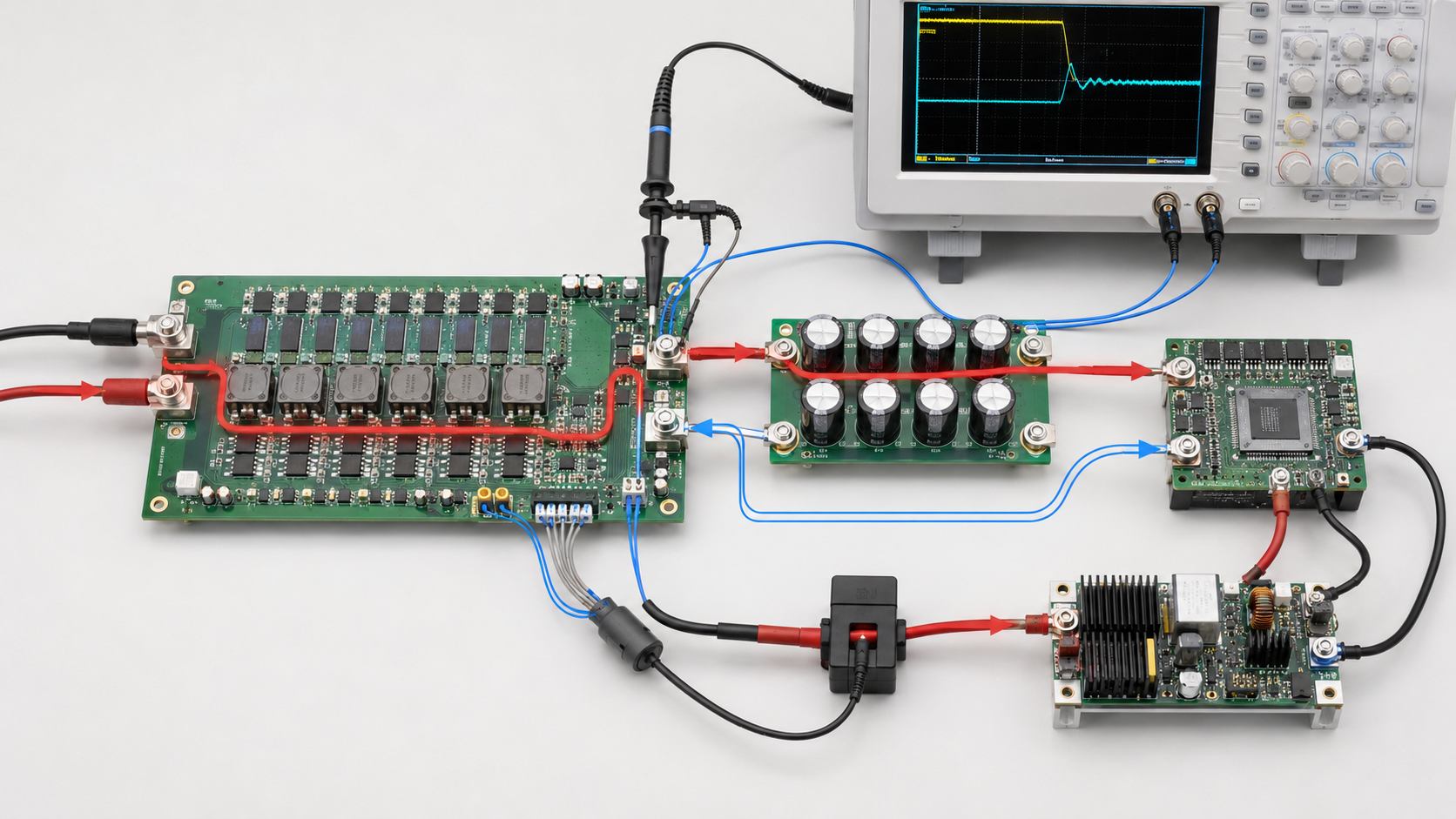
| Setup Element | Role in the Test | Risk if Poorly Implemented |
|---|---|---|
| Static load | Sets the base current operating point | Unrealistic base load can hide thermal or current-sharing problems |
| Dynamic load | Creates the fast current step | Long wiring or slow load edge can understate real transient stress |
| Oscilloscope voltage probe | Measures Vcore deviation and recovery | Long ground lead can create false ringing or exaggerated ripple |
| Current probe or shunt | Confirms load step amplitude and slew rate | Wrong bandwidth or shunt placement can distort current waveform |
| Remote sense point | Defines where the regulator controls the rail | Wrong sense location can make converter-side voltage look correct while ASIC-side voltage droops |
| Thermal condition | Represents airflow, board temperature, and component heating | Open-bench testing may not reflect enclosure or system airflow behavior |
Where to Probe: Converter Output, Capacitor Bank and ASIC Load Point
Probe location is one of the most important details in dynamic load response testing. The waveform at the converter output can differ from the waveform at the capacitor bank, and both can differ from the voltage at the ASIC sense point. A measurement that looks acceptable at the regulator output may still miss load-side droop after plane, via, package, or socket inductance.
A proper test plan usually includes more than one voltage measurement location. Converter-side probing shows how the regulator output behaves. Capacitor-bank probing shows how the decoupling network supports the current step. Load-side probing shows the voltage closest to the ASIC rail. Remote sense routing should be checked against the same physical locations.
| Probe Location | What It Shows | What It May Hide |
|---|---|---|
| Converter output | Regulator-side ripple, switching behavior, and bulk response | ASIC-side droop caused by plane and via inductance |
| Output capacitor bank | How the capacitor network supports load current | Voltage error at the ASIC package or load pins |
| Remote sense point | Voltage at the regulated feedback location | Local high-frequency noise at other pins if sense placement is incomplete |
| ASIC load-side rail | Closest practical view of the voltage seen by the device | Converter output stability details unless measured separately |
| Dynamic load terminals | Voltage at the artificial load connection | Real ASIC package and board distribution behavior |
Reading the Waveform: Undershoot, Overshoot and Recovery Time
During a load increase, the output rail usually dips before the control loop and power stages increase delivered current. The first voltage movement is strongly affected by capacitor ESR, ESL, mounting inductance, current path, and local decoupling. The later recovery shape depends on the converter control loop, phase response, inductor current ramp, and output capacitor network.
During load release, stored energy in inductors and capacitors can create overshoot. A good waveform should remain within the rail tolerance window, recover without excessive ringing, and show repeatable behavior across load levels, input voltages, temperatures, and airflow conditions.
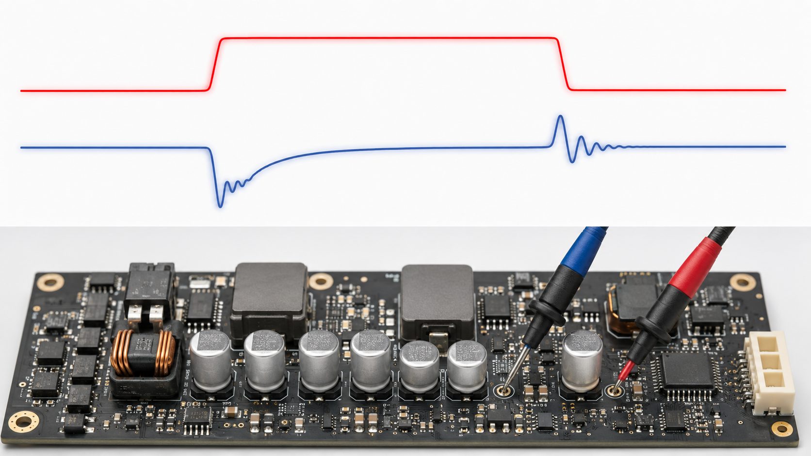
| Waveform Feature | Possible Cause | Engineering Check |
|---|---|---|
| Sharp initial droop | ESR, ESL, mounting inductance, local capacitor shortage | Check MLCC placement, via path, output capacitor mix, and probe loop |
| Slow recovery | Control-loop bandwidth, inductor current ramp, compensation, phase response | Review loop response, controller settings, inductor value, and load-line configuration |
| Large overshoot after load release | Stored energy, control response delay, insufficient damping | Check compensation, output capacitance, ESR damping, and load-dump behavior |
| High-frequency ringing | Probe inductance, PDN resonance, capacitor anti-resonance, switch-node coupling | Repeat with low-inductance probe tip and compare locations |
| Different results at different locations | Plane impedance, remote sense routing, local decoupling distribution | Measure converter output, capacitor bank, and ASIC sense point separately |
| Non-repeatable waveform | Thermal drift, unstable load trigger, measurement noise, marginal loop stability | Repeat across load levels, temperatures, and trigger settings |
Output Capacitors vs Control Loop
Output capacitors and the control loop perform different parts of the transient response. Capacitors supply immediate current during the earliest part of the load step. The control loop then changes the power-stage duty cycle and inductor current to restore the rail. A converter can fail dynamic testing if either side is weak.
Adding output capacitors can reduce droop and lower impedance in certain frequency regions, but it can also shift resonance, change damping, and affect loop stability. A capacitor network should be evaluated with effective capacitance, ESR, ESL, package size, placement, and load-side decoupling. For early transient sizing, the Decoupling Capacitor Calculator can estimate required capacitance from load step, allowed voltage droop, and response time.
| Transient Interval | Main Support Element | Design Sensitivity |
|---|---|---|
| First nanoseconds to early edge | ASIC-side MLCCs, package capacitors, mounted ESL path | Placement, via inductance, package inductance, probe method |
| Early microsecond region | MLCC arrays, polymer capacitors, power plane, current path | ESR, ESL, anti-resonance, remote sense, load-side distribution |
| Control recovery region | Controller, power stages, inductors, compensation, phase response | Loop bandwidth, phase margin, inductor current ramp, switching frequency |
| Thermal and repetitive operation | Power stages, inductors, bulk capacitors, airflow, PCB copper | Ripple current, temperature rise, lifetime, derating |
Bode Plot and Load-Step Testing
A Bode plot is useful for reviewing small-signal loop stability, crossover frequency, gain margin, and phase margin. It should not be treated as a complete substitute for large-signal dynamic load testing. Fast load steps can expose behavior that is influenced by capacitor placement, large-signal controller action, current limit behavior, dynamic load layout, and real board parasitics.
The PMP21887 test report makes this distinction explicit. In the Bode plot section, the report states that for constant on-time controllers, Bode plots can be used to predict stability, but not dynamic response; it also notes a difference between Bode-based timing expectation and the measured dynamic response timing. (TI Test Report, PMP21887)
| Method | Useful For | Limitation |
|---|---|---|
| Bode plot | Small-signal stability, crossover frequency, phase margin, gain margin | Does not fully represent large load-step behavior |
| Load-step waveform | Real undershoot, overshoot, ringing, recovery time, load-side behavior | Must be measured with correct probe location and realistic setup |
| PDN impedance simulation | Frequency-domain capacitor and plane impedance review | Depends on accurate models, layout extraction, and mounted parasitics |
| Thermal measurement | Power-stage, inductor, capacitor, and PCB heating under test conditions | Does not directly show fast voltage deviation |
Common Measurement Mistakes
Dynamic load response testing is sensitive to setup error. A waveform can look worse than the real rail if the probe loop is too large, and it can look better than the real rail if the measurement is taken far from the ASIC load point. The test should be designed to separate real converter behavior from measurement artifacts.
| Mistake | Effect on Result | Correction |
|---|---|---|
| Using a long oscilloscope ground lead | Adds false ringing and exaggerated noise | Use a short ground spring or coaxial low-inductance probe method |
| Measuring only at converter output | Can miss ASIC-side droop after board parasitics | Probe converter output, capacitor bank, and load-side sense point |
| Dynamic load placed far from rail | Slows the current edge and adds loop inductance | Place dynamic load close to the tested rail or account for interconnect inductance |
| Insufficient probe bandwidth | Hides fast spikes or distorts rise-time measurement | Use probe and oscilloscope bandwidth suitable for the expected edge speed |
| Bandwidth limit enabled accidentally | Filters high-frequency ringing and ripple | Document bandwidth setting and repeat if needed at full bandwidth |
| Wrong current measurement location | Load step amplitude or slew rate may be misread | Measure current at the dynamic load path or calibrated shunt location |
| Testing at one current point only | Misses behavior at low, mid, high, and peak load conditions | Test multiple static load levels and step amplitudes |
| Ignoring temperature and airflow | Waveform may change after components heat up | Repeat transient tests under realistic thermal conditions |
PMP21887 as a Reference Measurement Case
PMP21887 provides a useful example of how a high-current ASIC rail can be tested beyond static current capability. TI's test report lists input voltage of 10 V to 14 V DC, an output voltage range of 0.8 V to 1.2 V DC, testing at a 0.85 V setting, and a maximum load current of 360 A static / 600 A peak. The required equipment list includes a lab 12 V 50 A source, electronic loads, signal generator for the onboard dynamic load, loop stability analyzer, thermal camera, oscilloscope, voltage/current meters or current shunts. (TI Test Report, PMP21887)
In the dynamic response section, TI reports testing with a 100 A load step applied on top of a 300 A static load. The short-term waveform description notes about 31 mV peak undershoot, a 67 ns 10% to 90% rise time, an estimated load slew rate of about 1200 A/µs, and settling to within less than 10 mV of the initial value in 2 µs.
| PMP21887 Test Detail | Engineering Interpretation |
|---|---|
| 300 A static load | Tests transient response from a high-current operating point, not from light load only |
| 100 A dynamic load step | Represents a large current transition added to an already loaded rail |
| About 31 mV peak undershoot | Shows the immediate voltage droop under the current step |
| 67 ns rise time | Indicates a very fast load edge that stresses local capacitance and layout |
| About 1200 A/µs slew rate | Shows the severity of the current transition |
| 2 µs settling within less than 10 mV | Shows how quickly the rail returns close to the initial level |
Practical Test Checklist
A useful test plan should define the rail requirement first, then define the load step, measurement points, environmental conditions, and pass/fail criteria. The waveform should be captured at enough locations to separate converter behavior, capacitor-network behavior, and load-side voltage behavior.
| Checklist Item | What to Confirm |
|---|---|
| Rail tolerance | Allowed minimum and maximum Vcore during transient and steady state |
| Static load condition | Base load current before the transient step |
| Load step amplitude | Current step matches realistic ASIC, FPGA, or processor operating transitions |
| Slew rate | Current edge speed is fast enough to stress local decoupling and layout |
| Undershoot limit | Vcore does not fall below the device tolerance window |
| Overshoot limit | Vcore does not exceed maximum safe voltage during load release |
| Recovery time | Rail returns within the defined settling band fast enough for system operation |
| Ringing behavior | No excessive oscillation, anti-resonance, or measurement-induced ringing |
| Probe locations | Converter output, capacitor bank, and ASIC load-side sense point are reviewed |
| Thermal condition | Test is repeated after temperature stabilizes and under realistic airflow |
| Repeatability | Waveforms are consistent across repeated pulses and load conditions |
Frequently Asked Questions
What is dynamic load response in a buck converter?
Dynamic load response is the output voltage behavior when load current changes quickly. It includes undershoot, overshoot, ringing, recovery time, and settling behavior.
Why is static load testing not enough for an ASIC Vcore rail?
Static load testing shows steady current capability, but ASIC current can change very quickly. Dynamic load testing reveals whether the rail stays within tolerance during fast load transitions.
What is load step slew rate?
Load step slew rate is the speed of current change during the transient. Higher slew rate creates more stress on local capacitors, power planes, package inductance, and the regulator control loop.
What causes undershoot in a buck converter?
Undershoot can be caused by insufficient local capacitance, high ESR, high ESL, mounting inductance, slow control-loop response, poor remote sense placement, or long current paths.
What causes overshoot after load release?
Overshoot can occur when stored energy in inductors and capacitors remains after the load current drops. Control-loop response, damping, and output capacitor network design influence the peak.
Where should Vcore be measured during load-step testing?
Measure at multiple points: converter output, output capacitor bank, remote sense location, and as close as practical to the ASIC load. The load-side measurement is usually the most relevant for device tolerance.
Why does oscilloscope probe grounding matter?
A long probe ground lead adds inductance and can create false ringing. Low-inductance probing is required for meaningful transient and ripple measurements.
How do output capacitors affect dynamic response?
Output capacitors supply immediate transient current, reduce rail impedance, and influence damping. Effective capacitance, ESR, ESL, placement, and DC bias all affect the measured waveform.
Is a Bode plot enough to validate dynamic response?
No. A Bode plot helps review small-signal stability, but large-signal load-step testing is still required to verify real undershoot, overshoot, ringing, and recovery behavior.
How should a high-current Vcore rail be tested?
Test static load, ripple, thermal behavior, phase current sharing, dynamic load response, multiple probe locations, multiple load levels, realistic airflow, and approved component alternatives.
Engineering Summary
Dynamic load response testing is a required validation step for low-voltage high-current buck converters used in ASIC, FPGA, processor, switch-chip, and accelerator Vcore rails. Static current capability does not confirm transient performance. A rail must be tested for load step amplitude, slew rate, undershoot, overshoot, ringing, recovery time, probe location, thermal condition, and repeatability.
The most useful waveform is measured at the correct physical location with a low-inductance probe method and a realistic current step. Output capacitors provide immediate current support, while the control loop restores the rail. The final result depends on capacitor network design, power-stage response, inductor behavior, remote sense routing, PCB parasitics, measurement setup, and thermal operating condition.


