
 My Inquiry
 My Account


LDO Regulator: Dropout Voltage, Noise, PSRR and Power Dissipation
Article Details
An LDO regulator is a low-dropout linear voltage regulator. It provides a stable DC output voltage from a higher input voltage, even when the input voltage is only slightly above the output voltage. LDOs are widely used for MCU rails, analog circuits, sensors, RF modules, ADCs, DACs, PLLs, clocks, audio circuits and post-regulation after switching converters.
The main advantage of an LDO is simplicity and clean output. It usually needs fewer external parts than a switching regulator and can provide low-noise power for sensitive loads. The main limitation is heat. The voltage difference between input and output is burned as power inside the regulator, so an LDO is efficient only when the input-to-output voltage drop and load current are reasonable.
What Is an LDO Regulator?
An LDO regulator is a type of linear regulator designed to keep regulating with a small voltage headroom between input and output. A standard linear regulator may need a larger voltage difference to stay in regulation. An LDO reduces that required headroom, making it useful in battery-powered systems and low-voltage rails.
For example, a circuit that needs 3.3 V from a falling battery or from a 3.8 V intermediate rail may not work well with a regulator that needs 1 V or 2 V of headroom. A suitable LDO can keep the 3.3 V rail stable until the input voltage gets much closer to the output voltage.
| Term | Meaning | Design Check |
|---|---|---|
| LDO | Low-dropout linear regulator. | Check dropout voltage at the actual load current, not only the headline value. |
| Dropout voltage | Minimum input-to-output voltage difference required to keep regulation. | Compare worst-case input voltage against output voltage plus dropout margin. |
| Line regulation | Output change caused by input voltage change. | Useful when the input rail varies widely. |
| Load regulation | Output change caused by load current change. | Important for MCU, RF, motor-control and pulsed-load circuits. |
| PSRR | Power supply rejection ratio. | Shows how well the LDO rejects input ripple at a specified frequency and load condition. |
How an LDO Regulator Works
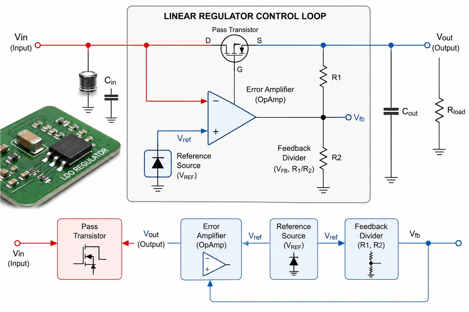
An LDO uses a voltage reference, an error amplifier, a pass transistor and a feedback path. The reference provides a stable comparison point. The error amplifier compares the feedback voltage with the reference. The pass transistor adjusts how much current flows from input to output. The output capacitor helps the loop stay stable and respond to load changes.
In a fixed-output LDO, the feedback divider is usually inside the IC. In an adjustable LDO, the output voltage is set by external feedback resistors. The same basic loop still applies: the regulator changes the pass device drive until the feedback voltage matches the internal reference.
Dropout Voltage
Dropout voltage is the minimum difference between input voltage and output voltage that the LDO needs to stay in regulation. If the input voltage falls too close to the output voltage, the regulator can no longer control the output. At that point, output voltage begins to fall with the input voltage.
Dropout voltage depends strongly on load current. A datasheet may show a very low dropout number at light load, but a much higher value at full load. For design work, use the dropout value specified at the expected load current, temperature range and output voltage condition.
| Example Condition | What Happens | Design Action |
|---|---|---|
| Input voltage well above output voltage | LDO has enough headroom and regulates normally. | Check heat, PSRR and maximum input voltage. |
| Input voltage close to output voltage | Dropout margin becomes small. | Check worst-case Vin, Vout tolerance, load current and temperature. |
| Input voltage below output plus dropout | LDO falls out of regulation. | Output voltage may sag; circuit may reset, misread ADC data or lose RF performance. |
A quick margin check is:
Dropout margin = Vin(min) - Vout - Vdropout(max)
Positive margin means the LDO should stay in regulation under that condition. Zero or negative margin means the output rail can drop out. The LDO Performance Calculator can estimate dropout margin, power dissipation, efficiency, PSRR ripple reduction and current-limit margin in one check.
LDO Dropout Voltage Video
The video above from Texas Instruments gives a practical explanation of LDO dropout voltage and why input headroom must be checked before selecting a regulator.
LDO Power Dissipation and Thermal Design
An LDO turns the voltage difference between input and output into heat. This is the most common reason an LDO that looks acceptable on paper fails in hardware. A small SOT-23 or DFN package may not survive a large voltage drop at high load current unless the PCB provides enough copper area for heat spreading.
The basic loss estimate is:
Power dissipation ≈ (Vin - Vout) × Iout
For example, regulating 5 V down to 3.3 V at 500 mA creates about 0.85 W of heat. That is already too much for many small packages without strong thermal layout. Regulating 12 V down to 3.3 V at the same current would create about 4.35 W, which is usually not a good LDO use case.
| Input | Output | Load | Approximate LDO Heat | Practical Meaning |
|---|---|---|---|---|
| 5 V | 3.3 V | 100 mA | 0.17 W | Often manageable with a suitable package and layout. |
| 5 V | 3.3 V | 500 mA | 0.85 W | Thermal check is required; small packages may run hot. |
| 12 V | 3.3 V | 500 mA | 4.35 W | Usually better handled by a buck converter or a buck plus LDO post-regulator. |
| 3.8 V | 3.3 V | 200 mA | 0.10 W | Good LDO use case when dropout margin is sufficient. |
Junction temperature depends on power dissipation, package thermal resistance, copper area, airflow, ambient temperature and board layout. The datasheet thermal resistance is only a starting point; a real PCB with poor copper can run hotter than expected.
LDO Efficiency
LDO efficiency is roughly output voltage divided by input voltage, when quiescent current is small compared with load current. This means an LDO can be efficient when Vin is close to Vout. It becomes inefficient when the voltage drop is large.
A 3.3 V output from 3.8 V input can be efficient enough for many low-noise rails. A 3.3 V output from 12 V input wastes most of the input power as heat. This is why LDOs are often used after a buck converter: the buck handles the large voltage reduction efficiently, and the LDO cleans up the final sensitive rail.
| Use Case | LDO Fit | Reason |
|---|---|---|
| Battery 4.2 V to 3.3 V sensor rail | Good | Small voltage drop, simple design and low noise. |
| Buck 3.8 V to 3.3 V RF rail | Good | LDO can reduce ripple and provide a clean local rail. |
| 12 V to 5 V at high current | Poor | Large heat loss; buck converter is usually preferred. |
| USB 5 V to 3.3 V low-current MCU rail | Often acceptable | Simple and low noise if load current is modest. |
PSRR and Low-Noise Performance
PSRR, or power supply rejection ratio, tells how much input ripple is rejected by the LDO. It is usually shown in dB across frequency. A high PSRR number at 100 Hz does not guarantee strong rejection at 1 MHz. PSRR changes with frequency, load current, input-output headroom, output capacitor network and layout.
Output noise is different from PSRR. Noise is generated inside the regulator itself, mainly from the reference, amplifier and pass device. PSRR describes how well the LDO blocks noise already present on the input rail. A good low-noise LDO should be checked for both output noise and PSRR at the frequency range that matters to the load.
| Parameter | What It Means | Where It Matters |
|---|---|---|
| Output noise | Noise produced by the LDO output itself. | ADC, DAC, RF, clock, PLL, VCO, audio and sensor rails. |
| PSRR | Ability to reject ripple or noise from the input supply. | Post-regulation after buck converters, noisy USB rails or shared power systems. |
| Noise spectral density | Noise level across frequency. | RF and high-resolution analog circuits. |
| Bypass / noise-reduction pin | Optional capacitor pin used by some LDOs to reduce reference noise. | Low-noise analog rails where startup time and noise trade-offs are acceptable. |
Analog Devices notes that LDO noise and PSRR behavior are especially relevant for high-speed clocks, ADCs, DACs, VCOs and PLLs. In those circuits, a power rail can directly affect jitter, phase noise, conversion accuracy or dynamic range. (ADI AN-1329)
Output Capacitor and Stability
The output capacitor is not only a bulk energy part. It is part of the LDO control loop. Wrong capacitance, wrong ESR, poor placement or excessive DC bias reduction can cause unstable output, ringing or oscillation.
Modern LDOs often support ceramic output capacitors, but the required value must still be checked in the datasheet. A capacitor marked 10 µF may provide much less effective capacitance under DC bias, especially in small MLCC packages. The MLCC DC Bias Calculator can help estimate how package size, dielectric and applied voltage may reduce usable capacitance before hardware validation.
| Capacitor Item | Design Check |
|---|---|
| Output capacitance | Use the datasheet minimum effective capacitance, not only the printed capacitor value. |
| ESR range | Some older LDOs need ESR within a stable range; some newer parts work with low-ESR ceramic capacitors. |
| DC bias | MLCC capacitance can drop sharply when DC voltage is applied. |
| Placement | Place the input and output capacitors close to the LDO pins with short return paths. |
| Load transient | Capacitor value and ESR affect voltage dip and recovery when load current changes quickly. |
| Temperature | Capacitance and ESR vary across temperature and dielectric type. |
LDO Regulator Circuit
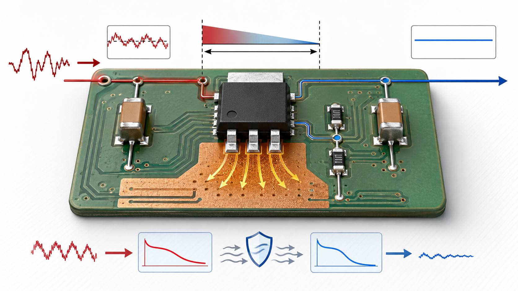
A basic fixed-output LDO circuit uses input capacitor, output capacitor and the LDO IC. Some devices also include enable, power-good, bypass, soft-start or noise-reduction pins. For adjustable-output LDOs, two feedback resistors set the output voltage.
The common adjustable LDO equation is:
Vout = Vref × (1 + R2 / R1)
Some regulators include feedback pin current or use different resistor naming conventions, so the exact datasheet equation should be followed. The Adjustable LDO Output Voltage Calculator can estimate Vout from R1, R2 and Vref, or calculate a resistor value for a target output voltage.
| Circuit Part | Purpose | Design Note |
|---|---|---|
| Input capacitor | Stabilizes the input rail near the LDO. | Place close to Vin and ground pins. |
| Output capacitor | Supports loop stability and transient response. | Use datasheet-recommended capacitance and ESR range. |
| Enable pin | Turns the LDO on or off. | Check logic threshold, leakage and startup sequence. |
| Feedback resistors | Set adjustable LDO output voltage. | Use proper tolerance and check feedback current or adjust-pin current. |
| Bypass / NR capacitor | Reduces reference noise in some low-noise LDOs. | Can affect startup time and transient behavior. |
| Power-good pin | Indicates when output is in range. | Useful for sequencing MCU, FPGA or RF rails. |
LDO vs Buck Converter
An LDO and a buck converter both regulate voltage, but they solve different problems. A buck converter is usually better for large voltage drops and high current. An LDO is usually better for simple, quiet, low-to-medium current rails where heat is acceptable.
| Item | LDO Regulator | Buck Converter |
|---|---|---|
| Efficiency | Depends mainly on Vout/Vin; poor when voltage drop is large. | Usually high across large voltage drops. |
| Noise | Low output noise possible, no switching ripple. | Has switching ripple and EMI that require layout and filtering control. |
| External parts | Usually simple: capacitors and optional feedback resistors. | Requires inductor, diode or synchronous switch, capacitors and careful layout. |
| Heat | Can be high when Vin - Vout is large. | Usually lower heat at high current. |
| Best use | Low-noise rails, post-regulation, small sensors, analog and RF rails. | Main power conversion, high-current rails and large step-down ratios. |
A common power architecture uses both. A buck converter generates an efficient intermediate rail, and an LDO generates the final clean supply for analog, RF or clock circuitry.
Quiescent Current and Battery Systems
Quiescent current is the current the LDO uses to operate itself. It matters in battery-powered devices, sleep-mode systems, remote sensors, meters and IoT nodes. A regulator with low dropout but high quiescent current may still waste too much battery energy during standby.
For always-on rails, check quiescent current across temperature and input voltage. For shutdown rails, check shutdown current and enable-pin leakage. In low-power systems, regulator self-consumption can be as important as load current.
| System Type | Important LDO Parameter |
|---|---|
| Always-on RTC or sensor rail | Very low quiescent current and stable light-load operation. |
| Battery MCU rail | Dropout voltage, quiescent current and shutdown current. |
| RF receive rail | Low noise, PSRR, transient response and thermal behavior. |
| High-current digital rail | Thermal limit, dropout margin, load transient and current limit. |
Common LDO Applications
LDO regulators are used when a clean local rail is more important than maximum efficiency, or when the input voltage is already close to the required output voltage. They are also used to isolate sensitive circuits from noisy shared rails.
| Application | Why an LDO Is Used | Key Selection Point |
|---|---|---|
| MCU 3.3 V rail | Simple regulation from USB, battery or intermediate rail. | Dropout voltage, output current, quiescent current and reset behavior. |
| ADC / DAC supply | Cleaner analog power rail. | Noise, PSRR, output impedance and load transient response. |
| RF module | Reduces supply noise that can affect RF performance. | Noise, PSRR at RF-related frequencies, thermal behavior and startup sequencing. |
| PLL / clock rail | Cleaner supply can reduce jitter sensitivity. | Output noise, PSRR and capacitor layout. |
| Sensor supply | Stable local rail for measurement accuracy. | Output accuracy, noise, quiescent current and load regulation. |
| Post-regulator after buck | Filters switching ripple and creates a quiet final rail. | PSRR at switching frequency, headroom, heat and transient response. |
How to Select an LDO Regulator
LDO selection starts with the power path. Check the worst-case input voltage, target output voltage, maximum load current and ambient temperature first. Then check dropout margin and heat. After the rail can survive electrically and thermally, check noise, PSRR, stability, package and protection functions.
| Selection Item | What to Check in the Datasheet |
|---|---|
| Input voltage range | Absolute maximum rating and recommended operating range. |
| Output voltage | Fixed value or adjustable range, tolerance and temperature drift. |
| Output current | Continuous load current, current limit and thermal shutdown behavior. |
| Dropout voltage | Specified value at actual load current and temperature. |
| Power dissipation | Loss from voltage drop and load current, including quiescent current when relevant. |
| Thermal resistance | Package and PCB thermal path to keep junction temperature within limit. |
| PSRR | Rejection at the ripple frequency that matters to the system. |
| Output noise | RMS noise, noise density and bypass capacitor option for sensitive rails. |
| Output capacitor requirement | Minimum effective capacitance, ESR range, capacitor type and placement. |
| Quiescent current | Self-consumption in active and shutdown modes. |
| Protection features | Thermal shutdown, current limit, reverse current protection and short-circuit behavior. |
| Grade and availability | Industrial or automotive grade, lifecycle status, package availability and second-source options. |
LDO Layout Notes
A good LDO layout keeps current loops short and gives heat a way out. Place input and output capacitors close to the regulator pins. Use a low-impedance ground return. Connect exposed pads to copper as recommended by the datasheet. Keep noisy switching nodes away from low-noise output rails.
| Layout Area | Practical Rule |
|---|---|
| Input capacitor | Place near Vin and ground to reduce input rail disturbance. |
| Output capacitor | Place near Vout and ground to support stability and transient response. |
| Thermal copper | Use copper area and vias to spread heat from the package. |
| Feedback trace | Keep away from noisy traces; connect to the output sense point where the datasheet recommends. |
| Grounding | Use a clean return path for analog or RF rails. |
| Post-buck filtering | Separate switching converter high di/dt loops from the LDO clean output rail. |
Common LDO Design Mistakes
Many LDO problems come from using the part as a simple three-pin voltage block and ignoring the datasheet conditions. The part may still output the right voltage during a light bench test, then fail during temperature, load transient or production variation.
| Mistake | Result | Better Check |
|---|---|---|
| Using dropout value without load condition | Output drops out at full load or low battery. | Use dropout at maximum load current and temperature. |
| Ignoring thermal loss | Regulator overheats or enters thermal shutdown. | Calculate power loss and junction temperature. |
| Choosing output capacitor by nominal value only | Effective capacitance is too low under DC bias. | Check effective capacitance and ESR. |
| Assuming high PSRR at all frequencies | Switching ripple passes into analog or RF rail. | Read the PSRR curve at the actual ripple frequency. |
| Replacing an LDO only by voltage and current | Stability, noise, pinout, package or thermal behavior changes. | Compare the full datasheet and validate the circuit. |
Frequently Asked Questions
What does LDO stand for?
LDO stands for low-dropout regulator. It is a linear voltage regulator that can regulate with a small voltage difference between input and output.
Is an LDO the same as a linear regulator?
An LDO is a type of linear regulator. Its main feature is lower dropout voltage than older or standard linear regulator designs.
What is dropout voltage in an LDO?
Dropout voltage is the minimum input-to-output voltage difference needed for the LDO to keep regulating. It should be checked at the actual load current and temperature.
Why does an LDO get hot?
An LDO gets hot because it dissipates the voltage difference between input and output as heat. Higher load current and larger voltage drop create more heat.
How do I calculate LDO power dissipation?
A basic estimate is power dissipation ≈ (Vin - Vout) × Iout. Quiescent current can be added for more accurate low-power calculations.
What is PSRR in an LDO?
PSRR is power supply rejection ratio. It shows how well the LDO reduces ripple or noise from the input supply, usually across frequency.
Is low noise the same as high PSRR?
No. Low noise means the LDO generates little output noise itself. High PSRR means it rejects noise already present on the input rail.
What capacitor does an LDO need?
Most LDOs require input and output capacitors. The datasheet specifies capacitance, ESR, type and placement requirements. Ceramic capacitors may lose effective capacitance under DC bias.
Can an LDO reduce switching regulator noise?
Yes, an LDO is often used after a buck converter to reduce ripple and provide a clean local rail. PSRR at the buck switching frequency must be checked.
When should I use an LDO instead of a buck converter?
Use an LDO when the voltage drop is small, the load current is modest, low noise is important, and heat is manageable. Use a buck converter for large voltage drops or high current.
How do I choose a 3.3 V LDO?
Check input voltage range, 3.3 V output tolerance, dropout voltage at load current, package thermal limit, quiescent current, PSRR, output noise and capacitor requirements.
Can I replace one LDO with another?
Only after checking pinout, package, output voltage, current rating, dropout voltage, stability capacitor, PSRR, noise, protection features and thermal behavior.
Engineering Summary
An LDO regulator is a simple and useful way to generate a clean voltage rail when the input voltage is close enough to the output voltage. It is commonly used for MCU, analog, RF, sensor, clock, ADC, DAC and post-buck power rails.
The key checks are dropout voltage, dropout margin, power dissipation, junction temperature, PSRR, output noise, output capacitor stability, quiescent current and package thermal layout. A good LDO design is not just a voltage match. It must stay in regulation, stay cool, remain stable and provide the noise performance required by the load.


