
 My Inquiry
 My Account


Logic Level Shifter: How to Connect 3.3V and 5V Logic Safely
Article Details
A logic level shifter transfers a digital signal between circuits that use different voltage domains. The decision to add one is not based on the rail labels alone. A 3.3 V output can drive some 5 V inputs directly and fail completely with others; a 5 V output can permanently overstress one 3.3 V input while being harmless to another that is explicitly 5 V tolerant.
The safe interface is found by comparing guaranteed output levels, receiver thresholds, input-voltage limits, signal direction and timing. That check also determines whether the right circuit is a direct wire, a resistor divider, a logic buffer, a dual-supply translator or an open-drain MOSFET level shifter.
What Does a Logic Level Shifter Do?
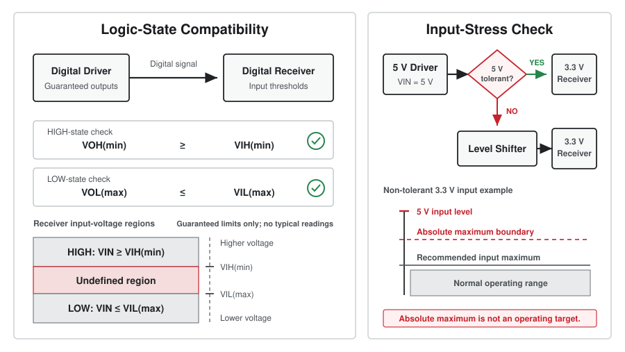
A digital receiver does not measure a signal as an exact voltage. It recognizes a LOW below its specified input-low limit, VIL(max), and a HIGH above its input-high limit, VIH(min). The region between those limits is undefined. Noise, temperature and production variation can move a marginal signal across the switching point even when a bench prototype appears to work.
The driver has its own guaranteed limits. VOH(min) is the lowest voltage it promises while sourcing the stated current; VOL(max) is the highest voltage it permits while sinking the stated current. Typical oscilloscope readings are not substitutes for these guaranteed values.
| Data-sheet item | Belongs to | Design use |
|---|---|---|
| VOH(min) | Driver | Must exceed the receiver's VIH(min) with positive noise margin. |
| VOL(max) | Driver | Must remain below the receiver's VIL(max). |
| VIH(min) | Receiver | Minimum guaranteed input voltage recognized as HIGH. |
| VIL(max) | Receiver | Maximum guaranteed input voltage recognized as LOW. |
| Recommended input range | Receiver | Voltage range allowed during normal operation. |
| Absolute maximum input voltage | Receiver | Stress boundary, not a valid operating target. |
| IOFF or partial-power-down rating | Receiver or translator | Shows whether an input may remain driven while that device or rail is off. |
The two basic DC margins are:
LOW-state margin = VIL(max) − VOL(max)
Both results must be positive at the actual supply voltages, load currents and temperature range. Extra margin is desirable where traces are long, ground noise is significant or edges are exposed to switching transients.
Can 3.3 V Logic Drive a 5 V Input Directly?
Sometimes. The deciding comparison is the 3.3 V driver's VOH(min) against the 5 V receiver's VIH(min). A 5 V CMOS input whose HIGH threshold is specified near 0.7 × VCC may require about 3.5 V, which a 3.3 V source cannot guarantee. A 5 V device with a TTL-compatible input threshold may accept the same signal because its guaranteed VIH(min) is lower. The exact part number and manufacturer data sheet decide the result.
For example, a driver guaranteed to produce 2.4 V under its specified load does not reliably drive a receiver requiring at least 3.5 V:
If the receiving device instead guarantees HIGH recognition from 2.0 V, the same driver has 0.4 V of stated HIGH margin. Output loading, supply tolerance and temperature still belong in the check.
This issue appears in real mixed-voltage chains. A 3.3 V microcontroller cannot be assumed to drive a 5 V power shift register merely because both use digital control pins. The 74HC595 and TPIC6B595 comparison, for example, shows why the TPIC6B595 control interface needs a separate threshold review even though its shift-register operation resembles the 74HC595.
Can a 5 V Output Drive a 3.3 V Input?
Only when the 3.3 V input is explicitly rated to accept that voltage. "5 V tolerant" must appear in the data sheet for the applicable pins and operating state. Some microcontrollers make only selected GPIO pins tolerant; analog inputs, oscillator pins, reset pins and USB-related pins may follow different limits.
A clamp diode inside a non-tolerant input can conduct when the signal rises above the local supply. The resulting injection current may lift the 3.3 V rail, back-power an unpowered IC, corrupt nearby analog circuitry or exceed an input-current limit. A series resistor can limit current in certain clamp-based interfaces, but it does not automatically make the operating condition valid. The data sheet must authorize that mode and specify the allowable injection current.
Logic Level Shifter Circuit Options
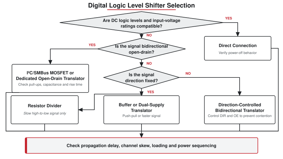
Direction, output topology and edge rate eliminate most unsuitable circuits before a part number is considered.
| Method | Direction | Good fit | Main limitation |
|---|---|---|---|
| Direct connection | Fixed | Thresholds and input ratings already match | Compatibility must be proved for both logic states and power conditions |
| Two-resistor divider | High voltage to low voltage | Slow push-pull control, status or UART-like signals | RC loading slows edges; cannot translate LOW to HIGH |
| Single-supply logic buffer | Fixed | Clean up- or down-translation when its input thresholds and tolerance fit | One output-voltage domain; logic-family details matter |
| Dual-supply direction-controlled translator | Fixed or switched with DIR | Push-pull GPIO, UART, SPI and control buses | Direction and output-enable sequencing must be defined |
| Auto-direction translator | Bidirectional | Interfaces supported by the selected translator architecture | External pull-ups, capacitive loads and strong drivers can conflict with some families |
| Discrete N-channel MOSFET | Bidirectional open-drain | I²C and SMBus at validated bus speed | Not a universal push-pull GPIO, UART or SPI translator |
Using a Resistor Divider for 5 V to 3.3 V Logic
A resistor divider is useful when the source is push-pull, the signal travels in one direction and the required edge rate is modest. Connect R1 from the 5 V driver to the receiver node and R2 from that node to ground:
With R1 = 5.1 kΩ and R2 = 10 kΩ, an unloaded 5.0 V HIGH becomes approximately 3.31 V. The divider draws about 0.33 mA while the source is HIGH.
The ratio is only the DC part of the design. Receiver leakage and any internal pull resistor alter the loaded voltage, while input and trace capacitance slow the edge. The receiver sees the divider's Thevenin resistance:
For 5.1 kΩ and 10 kΩ, RTH is about 3.38 kΩ. With 20 pF of combined input, trace and probe capacitance, the first-order time constant is about 67.5 ns. A 10% to 90% transition takes roughly 2.2 time constants, or about 149 ns. That may be harmless on a slow enable line and unacceptable on a fast clock.
The Aetrix voltage divider calculator can check the resistor ratio. For digital use, follow the ratio calculation with an RC edge-rate check; the RC time-constant calculator provides the first-order value when the effective source resistance and bus capacitance are known.
Do not use this divider as a bidirectional I²C level shifter. It permanently loads the line, gives the wrong behavior when either side needs to pull LOW and couples the two voltage domains through a fixed ratio. It is also a poor choice for a high-speed clock whose receiver has tight rise-time or duty-cycle requirements.
Buffers and Dedicated Voltage Translators
Single-supply buffers
A buffer powered from the destination rail can provide a restored full-swing output. For 3.3 V-to-5 V conversion, its inputs must guarantee a HIGH at the source's minimum output level while the buffer runs from 5 V. TTL-compatible HCT or AHCT inputs are often used for this job, but the full data sheet-not the family letters alone-must confirm thresholds, supply range, timing and input behavior.
For 5 V-to-3.3 V conversion, a buffer powered at 3.3 V needs inputs specified as 5 V tolerant. Its 3.3 V output then presents a normal logic swing to the destination. Check whether the input remains tolerant when the buffer supply is off.
Dual-supply, direction-controlled translators
A dual-supply translator establishes one logic domain on each side. Devices such as a single-bit 74LVC1T45 use VCCA, VCCB and a DIR input to set the transfer direction. This architecture suits push-pull buses because the active direction is explicit and each output is driven to the rail of its own domain.
DIR must not change while two external drivers are active on the same line. If the selected translator also provides OE, use it to place the ports in high impedance during startup, reset or direction reversal whenever the surrounding circuit could otherwise contend. Verify which supply powers each control pin; it is not necessarily referenced to the rail that is most convenient for the controller.
Auto-direction translators
"Automatic bidirectional" describes several different internal architectures, not one interchangeable behavior. Pass-FET devices depend on pull-ups or the connected drivers. Edge-accelerated translators detect transitions and briefly reinforce them. Their limits can include maximum lumped capacitance, restrictions on external pull-up values and minimum drive strength needed to reverse direction.
Choose the translator from its application table and loading conditions rather than from channel count and voltage range alone. A part advertised for both open-drain and push-pull signals may still require direction control whenever two push-pull outputs could oppose each other.
How the BSS138 Bidirectional Level Shifter Works
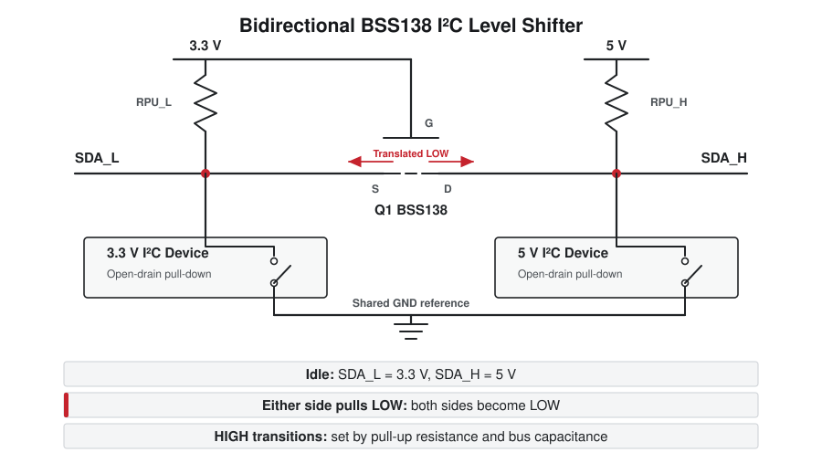
The common MOSFET level shifter uses one N-channel MOSFET per open-drain signal. For a 3.3 V-to-5 V I²C connection, the source connects to the 3.3 V side, the drain connects to the 5 V side and the gate is held at 3.3 V. Each side has its own pull-up resistor to its own supply.
- When neither side pulls LOW, both pull-ups hold their local bus nodes HIGH. VGS is approximately zero, so the MOSFET is off and each side rests at its own rail.
- When the 3.3 V side pulls LOW, VGS becomes positive. The MOSFET turns on and pulls the 5 V side LOW.
- When the 5 V side pulls LOW, the MOSFET body diode initially lowers the source-side voltage. This creates sufficient VGS to turn the channel on, after which both sides are held LOW.
- When the pulling device releases the line, the two pull-ups restore the HIGH levels. The rising edges are therefore passive RC transitions.
Why the BSS138 circuit is well suited to I²C
I²C devices use open-drain outputs. No device drives the line HIGH; it either pulls LOW or releases the bus. That behavior prevents a 3.3 V push-pull HIGH driver from fighting a 5 V LOW driver and lets the pass-MOSFET topology operate without a direction pin.
The pull-ups must satisfy both the LOW-state current limit and the permitted rise time. A useful first-order rise-time relationship for the 30% to 70% interval is:
Lower resistance produces a faster rise but increases the current that every device must sink during a LOW. Higher resistance reduces LOW-state current but may violate the I²C rise-time limit. Account for device pins, MOSFET capacitance, connectors, traces, cables and probes in CBUS. Calculate each voltage side separately because its pull-up and capacitance may differ.
Why it is not a universal bidirectional level converter
UART and conventional SPI outputs are push-pull. They actively drive both HIGH and LOW. Connecting two push-pull drivers through a passive bidirectional MOSFET network can create contention, distorted HIGH levels and poorly controlled direction changes. A BSS138 module may appear to pass a slow UART signal in one lab setup, but that does not make the topology valid across baud rate, capacitance, temperature and device variation.
For UART, treat TX and RX as two separate unidirectional signals and translate each in its fixed direction. For SPI, translate SCLK, MOSI and chip-select toward the peripheral, then translate MISO back toward the controller. A direction-controlled or channel-direction-specific translator makes those paths explicit.
Which Level Shifter Fits GPIO, UART, SPI and I²C?
| Interface | Electrical behavior | Suitable starting point | Critical check |
|---|---|---|---|
| Static GPIO or enable | Usually unidirectional push-pull | Direct connection, divider for down-shift, or single-channel buffer | Startup state and whether the line can reverse direction |
| UART | Separate push-pull TX and RX | Two unidirectional translator channels | Propagation delay and edge integrity at the selected baud rate |
| SPI | Fast push-pull signals with fixed directions | Direction-controlled or direction-specific translator | Clock delay, channel skew, MISO turn-off and bus contention |
| I²C or SMBus | Bidirectional open-drain | MOSFET/pass-FET or dedicated open-drain translator | Pull-up current, bus capacitance, rise time and VOL budget |
| One-wire open-drain control | Shared bidirectional line | Open-drain translator approved for the protocol | Idle level, timing recovery and pull-up placement |
| Fast memory or display bus | Multiple push-pull channels, sometimes changing direction | Purpose-built bus translator | Bandwidth, skew, direction timing, loading and power sequencing |
Three Practical 3.3 V and 5 V Interface Examples
3.3 V microcontroller to a 5 V CMOS control input
Read VOH(min) for the microcontroller at the intended source current and VIH(min) for the 5 V receiver. If the receiver uses a CMOS-ratio threshold that the controller cannot meet, use a 5 V-powered buffer with compatible input thresholds or a dual-supply translator. Do not rely on a typical 3.28 V scope reading.
5 V sensor output to a 3.3 V GPIO
If the GPIO is explicitly 5 V tolerant in every relevant power state, a direct connection may be valid. Otherwise, a resistor divider can serve a slow, fixed-direction push-pull output. A buffer or translator is preferable when the line is fast, the cable is long, the input capacitance is uncertain or edge timing matters.
5 V I²C sensor on a 3.3 V controller bus
First check whether the sensor can operate with pull-ups to 3.3 V even though its supply is 5 V; some devices accept that arrangement and need no translator. Confirm that the sensor has no internal pull-up to 5 V. If both sides require their own HIGH voltage, use an open-drain level shifter with separate pull-ups. Verify that neither side contains an incompatible push-pull accelerator and that the combined bus meets rise-time and LOW-level requirements.
Timing, Loading and Power-Sequencing Checks
Propagation delay and channel skew
A translator adds delay to the signal path. For a static enable pin, a few nanoseconds or tens of nanoseconds may be irrelevant. On SPI, delay through SCLK and the return delay through MISO reduce the controller's sampling margin. Multi-bit buses also need channel-to-channel skew limits, not just a headline maximum data rate.
Rise time is not the same as propagation delay
Propagation delay measures when an output crosses a defined threshold after the input event. Rise time measures how long the edge takes to move between two voltage percentages. A pass-FET I²C translator may add little intrinsic delay while still producing an edge that is too slow because the HIGH transition is set by pull-up resistance and capacitance.
Power-off isolation
Mixed-voltage rails rarely start and stop at exactly the same time. If side A is powered while side B is off, current can flow through input protection structures unless the device specifies partial-power-down behavior such as IOFF. A translator with power-off protection places its ports in high impedance under the stated conditions; a generic buffer may not.
Where the translator has OE, hold it in the disabled state with a resistor until both rails and the controller are valid. Also check supply-order requirements. Some dual-supply translators permit either rail to start first, while others prescribe a relationship between VCCA and VCCB.
Ground reference and transient voltage
Non-isolated logic-level translation assumes a shared reference. Ground offset subtracts directly from the receiver's noise margin. A remote board with long ground wiring, motor current or hot-plug transients may need a robust transceiver, common-mode-tolerant interface or galvanic isolation rather than a small logic translator.
Common Level-Shifting Failures
| Symptom | Likely cause | What to measure |
|---|---|---|
| 3.3 V HIGH is read intermittently by a 5 V input | Negative or inadequate HIGH-state margin | VOH at the driver pin, VIH requirement, supply tolerance and ground offset |
| 3.3 V rail rises when the board should be off | Back-powering through a driven input or translator port | Input current with the destination supply off and the device's IOFF rating |
| I²C works at 100 kHz but fails at 400 kHz | Pull-ups are too weak for the total bus capacitance | SDA/SCL 30%–70% rise time on both voltage domains |
| I²C bus does not return HIGH | Wrong MOSFET orientation, swapped rails, stuck device or missing or overly weak pull-up | Gate, source and drain DC voltages with devices disconnected in stages |
| UART data is corrupted only at higher baud rates | Divider RC delay or an unsuitable auto-direction translator | Edge time, threshold-crossing time and waveform at the receiving pin |
| SPI reads the wrong bits at high clock rate | Round-trip delay, skew or MISO contention | SCLK and MISO together at the controller, including chip-select timing |
| Signal overshoots the destination rail | Fast edge, long trace, poor return path or probe artifact | Waveform with a short ground spring at the receiver pin |
Logic Level Translator Selection Checklist
- Record the actual minimum and maximum voltage of both supply rails.
- Identify every signal as push-pull, open-drain or three-state.
- Mark the fixed direction of each channel and any direction changes during operation.
- Compare VOH(min), VOL(max), VIH(min) and VIL(max) at the stated currents.
- Check recommended input voltage, absolute maximum voltage and injection-current limits.
- Calculate rise time from source resistance or pull-up resistance and total capacitance.
- Budget propagation delay and channel skew at the real interface frequency.
- Review OE, DIR, pull resistors and safe states during reset, hot-plug and power sequencing.
- Confirm partial-power-down behavior if one voltage domain can be off independently.
- Use the exact manufacturer data sheet for package, pinout and operating-temperature limits.
Technical References
- Texas Instruments Voltage-Level Translation Guide
- Texas Instruments LSF0102 bidirectional translator information
- Nexperia 74LVC1T45 dual-supply translating transceiver
- NXP level-shifting I²C resources and AN10441
Frequently Asked Questions
What is the difference between a logic level shifter and a logic level converter?
For digital interfaces, the terms usually describe the same function: translating a logic signal between voltage domains. "Level shifter" is also used in analog and power circuits, so the interface type must be clear.
Do I need a level shifter from 3.3 V to 5 V?
Use one when the 3.3 V driver's guaranteed VOH(min) does not meet the 5 V receiver's VIH(min) with adequate margin. A direct connection is valid only when the exact data sheets prove compatibility.
Can I use a resistor divider as a logic level shifter?
Yes, for unidirectional high-to-low translation of a reasonably slow push-pull signal. Check the divider ratio, input loading and RC rise time. It cannot perform low-to-high translation or proper bidirectional I²C translation.
Is a BSS138 level shifter suitable for UART?
It is designed around open-drain behavior and is a poor general choice for push-pull UART. Translate TX and RX as separate fixed-direction signals with buffers or a translator intended for push-pull data.
Why does an I²C level shifter need pull-up resistors on both sides?
The MOSFET transfers LOW states, but it does not generate the HIGH voltage. Each pull-up restores its own side to that side's supply rail and sets the bus rise time and LOW-state sink current.
Can a 5 V-tolerant input be driven while its 3.3 V supply is off?
Not necessarily. Five-volt tolerance during normal operation does not guarantee power-off tolerance. Look for an IOFF or partial-power-down specification covering the unpowered state.
Does a level shifter make two circuits electrically isolated?
No. Ordinary level translators share a ground reference and do not provide galvanic isolation. Use a digital isolator or optocoupler architecture when ground separation or high common-mode voltage is required.
What should I probe when a level shifter does not work?
Measure both supply rails, OE and DIR, then view the input and output at the IC pins. Check HIGH and LOW levels, rise and fall times, propagation delay, bus contention and behavior while either voltage domain is powered down.


