
 My Inquiry
 My Account


Operational Amplifier (Op Amp): Basics, Configurations, Feedback and Applications
Article Details
An operational amplifier, or op amp, is a high-gain analog integrated circuit used to amplify, buffer, filter, compare or condition voltage signals. It is one of the most common building blocks in analog electronics because the same IC can support many circuit functions when combined with the correct feedback network.
Op amps are used in sensor interfaces, ADC front ends, audio circuits, active filters, current sensing, photodiode amplifiers, instrumentation systems, power-supply feedback loops and industrial measurement circuits. The final circuit behavior is not set by the op amp alone. It is set by the op amp, feedback resistors, input source, load, power rails, layout and real device limits.
What Is an Operational Amplifier?
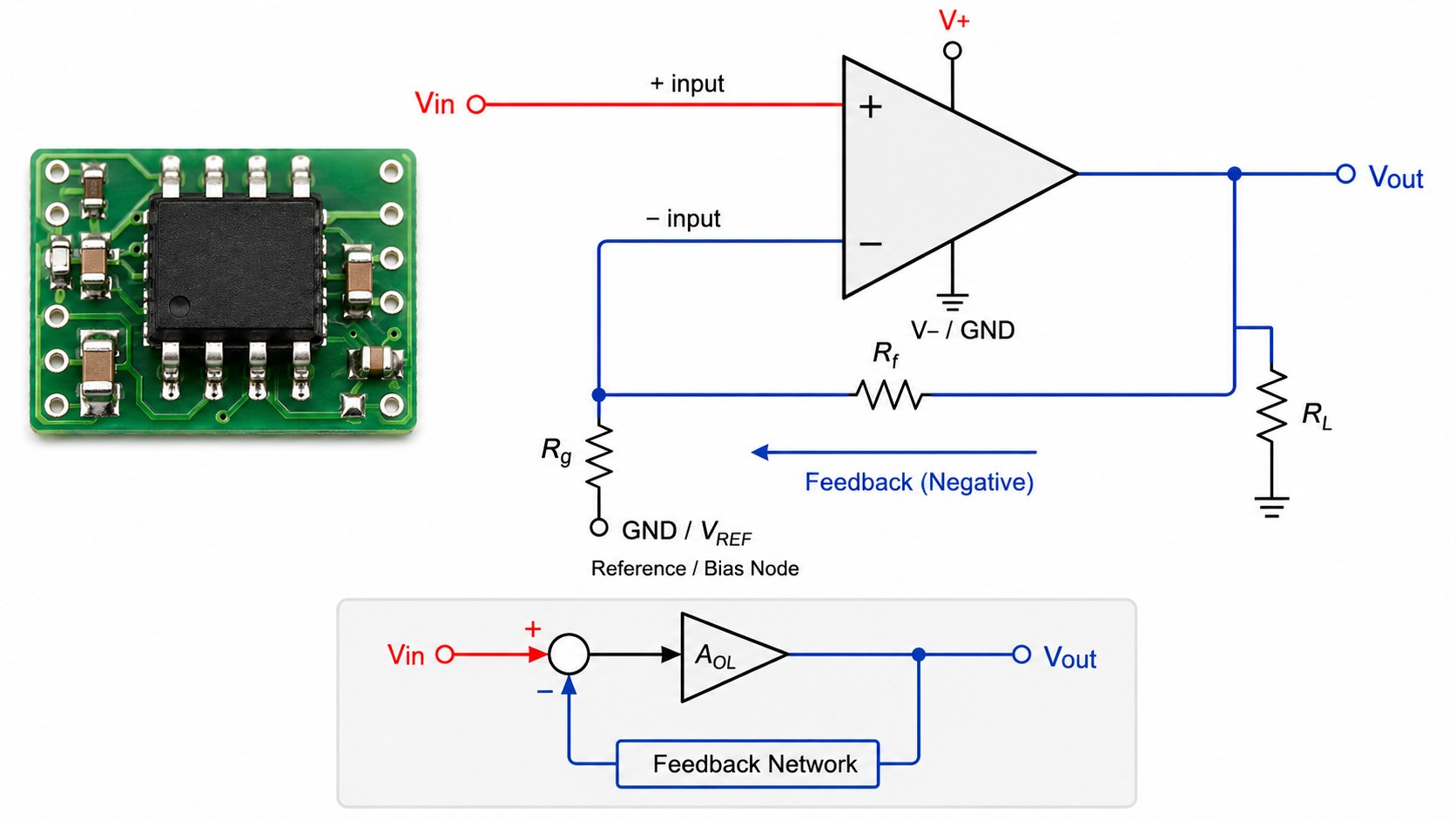
An operational amplifier is a differential-input, single-output analog amplifier. It has a non-inverting input, an inverting input and an output. The output responds to the voltage difference between the two inputs. In most practical circuits, negative feedback is used to control the gain and force the two input terminals to operate near the same voltage.
Without feedback, the open-loop gain of an op amp is very high. A tiny voltage difference between the inputs can push the output close to one supply rail. With feedback, the circuit becomes predictable: the external resistors, capacitors or other network components define the closed-loop gain, filter response or signal-conditioning function.
| Op Amp Pin / Function | Meaning | Design Check |
|---|---|---|
| Non-inverting input (+) | Output moves in the same direction as this input when feedback allows it. | Check input common-mode voltage range. |
| Inverting input (-) | Output moves in the opposite direction when this input rises relative to the non-inverting input. | Check feedback node impedance and bias-current error. |
| Output | Drives the load or next circuit stage. | Check output swing, output current, capacitive load and short-circuit behavior. |
| Power rails | Set the allowed voltage range for input and output operation. | Check single-supply, dual-supply and rail-to-rail limits. |
| Feedback network | Controls closed-loop gain, filter response or operating point. | Check resistor tolerance, capacitor tolerance, stability and noise contribution. |
Op Amp vs Operational Amplifier
Operational amplifier is the full name. Op amp, op-amp and opamp are common short forms. Datasheets may use terms such as operational amplifier, precision amplifier, low-noise amplifier, zero-drift amplifier, rail-to-rail amplifier or high-speed amplifier depending on the product family and target application.
The short name does not change the function. In engineering work, "op amp" usually refers to the same class of analog IC, but the actual device type still matters. A low-power CMOS op amp, a high-speed op amp, an audio op amp and a zero-drift precision op amp can have very different input structures, output stages and stability limits.
How an Op Amp Works
A simple way to understand an op amp is to treat it as a controlled output stage. The input pair senses the voltage difference between the two input pins. The internal gain stages amplify that difference. The output stage then drives the load. When negative feedback is connected, the output moves until the feedback input is driven to the correct voltage.
In a non-inverting amplifier, the output is fed back to the inverting input through a resistor divider. In an inverting amplifier, the input signal is applied through a resistor to the inverting node, and the feedback resistor returns output voltage to that same node. In a voltage follower, the output is connected directly to the inverting input, creating a buffer with unity gain.
Ideal Op Amp vs Real Op Amp
The ideal op amp model is useful for first-pass circuit analysis, but it is not enough for component selection. Analog Devices describes the ideal op amp as having infinite input impedance, infinite open-loop gain, zero output impedance, infinite bandwidth and zero noise; real op amps have finite limits that must be checked in actual circuits. (Analog Devices op amp glossary)
| Parameter | Ideal Op Amp | Real Op Amp | Why It Matters |
|---|---|---|---|
| Open-loop gain | Infinite | High but finite | Finite gain creates closed-loop gain error, especially at high frequency. |
| Input current | Zero | Input bias current flows | Bias current creates voltage error with high source resistance. |
| Input offset voltage | Zero | Small input-referred error voltage | Offset is amplified by closed-loop gain and can dominate precision circuits. |
| Bandwidth | Infinite | Limited by gain-bandwidth product and internal compensation | High closed-loop gain reduces usable bandwidth. |
| Slew rate | Infinite | Limited output voltage change rate | Large fast signals can distort even when small-signal bandwidth looks sufficient. |
| Output swing | Can reach both rails | Limited by output stage and load current | Single-supply circuits may clip before reaching ground or VCC. |
| Output current | Unlimited | Limited | Loads, ADC sampling capacitors and cables can exceed output drive capability. |
Open-Loop and Closed-Loop Operation
Open-loop operation means the op amp is used without feedback. Because open-loop gain is very high, the output usually saturates high or low when the input difference is small. This behavior is closer to comparator use than linear amplification. A standard op amp can sometimes be used as a simple comparator in slow, non-critical circuits, but a real comparator is usually better for fast switching, logic output, overdrive recovery and predictable threshold behavior.
Closed-loop operation uses feedback to control the output. Negative feedback reduces the effective gain, improves linearity, sets the bandwidth and makes the circuit behavior much more predictable. Most buffer, amplifier, filter, integrator and signal-conditioning circuits are closed-loop op amp circuits.
Operational Amplifier Video
The video above from Texas Instruments gives a useful introduction to op amps and the TI Precision Labs op amp curriculum. It is a practical reference before comparing closed-loop configurations, feedback, bandwidth, offset and stability.
Common Op Amp Configurations
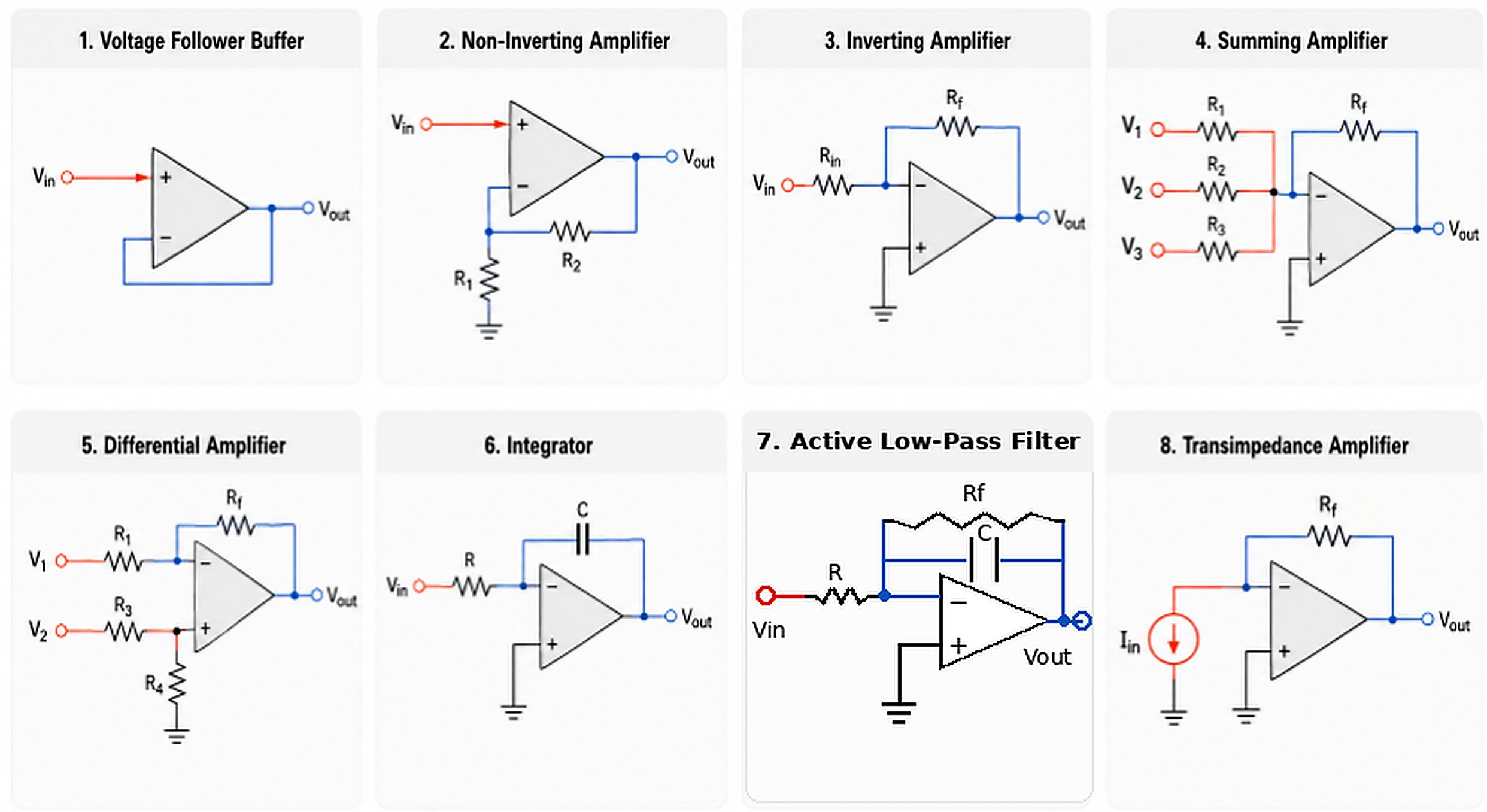
Op amp circuits are usually named by the feedback network and signal path around the amplifier. The same op amp can act as a buffer, voltage amplifier, summing amplifier, active filter, integrator or current-to-voltage converter when the surrounding components change.
| Configuration | Main Function | Typical Use | Key Check |
|---|---|---|---|
| Voltage follower / buffer | Gain of 1 with high input impedance and low output impedance. | Sensor buffering, voltage-divider buffering, ADC input drive. | Unity-gain stability, output current and capacitive load. |
| Non-inverting amplifier | Positive gain without phase inversion. | General signal amplification and high-impedance input stages. | Input common-mode range, gain-bandwidth product and output swing. |
| Inverting amplifier | Negative gain with 180-degree phase inversion. | Scaling, summing, active filters and signal inversion. | Input impedance, feedback resistor value and noise. |
| Summing amplifier | Adds multiple input signals. | Audio mixing, analog summing, control-signal combining. | Input resistor matching and output headroom. |
| Differential amplifier | Amplifies the voltage difference between two nodes. | Bridge sensors, low-side sensing, balanced signal measurement. | Resistor matching and common-mode voltage range. |
| Integrator | Output changes according to accumulated input over time. | Active filters, control loops, waveform shaping. | Input offset, leakage, saturation and reset path. |
| Active filter | Provides frequency-selective gain. | Low-pass, high-pass, band-pass and anti-alias filters. | Op amp bandwidth, capacitor tolerance and stability. |
| Transimpedance amplifier | Converts input current to output voltage. | Photodiodes, current-output sensors and optical receivers. | Input capacitance, feedback capacitor, noise and stability. |
Inverting and Non-Inverting Op Amp Circuits
The non-inverting amplifier keeps the output signal in phase with the input. It also provides high input impedance because the signal enters the non-inverting input. The closed-loop gain is set by the feedback divider from output to the inverting input.
The inverting amplifier applies the signal through an input resistor to the inverting node. The output is inverted relative to the input. Its input impedance is largely set by the input resistor, which can be useful when the source impedance and summing behavior must be controlled.
| Item | Non-Inverting Amplifier | Inverting Amplifier |
|---|---|---|
| Output phase | Same phase as input. | Inverted relative to input. |
| Input impedance | Very high in many cases. | Set mainly by input resistor. |
| Common use | Sensor amplification, high-impedance signal conditioning. | Scaling, summing, active filters and signal inversion. |
| Common mistake | Ignoring input common-mode range in single-supply circuits. | Using very large feedback resistors and creating noise or bias-current error. |
For quick resistor checks, the Non-Inverting Op-Amp Resistor Calculator can estimate feedback resistor values for a target gain, while the Inverting Op-Amp Resistor Calculator can support inverting gain and offset resistor selection. Final values should still be checked against input impedance, noise, tolerance and available standard resistor series.
Voltage Follower and Buffer Circuits
A voltage follower connects the op amp output directly to the inverting input. The output follows the non-inverting input, so the voltage gain is 1. The reason to use this circuit is not voltage gain; it is impedance isolation.
A buffer lets a high-impedance signal source drive a lower-impedance load. It is common after sensor outputs, resistor dividers, RC filters and reference nodes. It is also used before ADC inputs when the ADC sampling capacitor would otherwise disturb the signal source.
| Buffer Use Case | Why It Helps | Important Check |
|---|---|---|
| Voltage divider output | Prevents load current from changing the divider voltage. | Input bias current and output swing. |
| Sensor output | Protects weak sensor output from downstream loading. | Input common-mode range, offset and noise. |
| ADC input | Provides low source impedance for the ADC sampling capacitor. | Settling time, output current and capacitive load stability. |
| Reference voltage node | Allows a reference or divider to drive multiple loads. | Output noise and load transient behavior. |
Op Amp Offset, Bias Current and Accuracy
Input offset voltage is a small error voltage that appears as if it were applied between the op amp inputs. In high-gain circuits, this error can become large at the output. A 1 mV input offset becomes 100 mV of output error at a gain of 100.
Input bias current is the small current that flows into or out of the input pins. With low source resistance, it may be negligible. With high-value resistors, photodiodes, sensors or precision dividers, bias current can create measurable voltage error.
| Error Source | Where It Appears | Design Response |
|---|---|---|
| Input offset voltage | Output DC error after closed-loop gain. | Use precision, low-offset or zero-drift op amp where needed. |
| Offset drift | Error changes with temperature. | Check drift specification for industrial and automotive designs. |
| Input bias current | Voltage error across source or feedback resistance. | Use suitable input architecture and avoid unnecessarily large resistors. |
| Input offset current | Mismatch between two input bias currents. | Important in balanced resistor networks and precision differential circuits. |
| Resistor tolerance | Gain error and CMRR degradation. | Use precision resistors or matched resistor networks where required. |
Gain-Bandwidth Product and Slew Rate
Gain-bandwidth product, or GBW, links closed-loop gain with usable bandwidth. As closed-loop gain increases, available bandwidth decreases. A low-frequency sensor amplifier may work with a modest GBW device, while an audio stage, ADC driver or fast control-loop circuit needs more bandwidth margin.
Slew rate is the maximum rate at which the output voltage can change. It matters when the signal is large and fast. An op amp can have enough small-signal bandwidth but still distort a large output waveform if the required voltage change exceeds its slew rate.
| Parameter | Controls | Common Failure |
|---|---|---|
| GBW | How much bandwidth remains at the selected closed-loop gain. | Gain is correct at DC but rolls off too early at signal frequency. |
| Slew rate | How fast the output can move for large signals. | Large sine wave, pulse or audio signal becomes distorted. |
| Phase margin | Closed-loop stability. | Ringing or oscillation with capacitive load or high-speed layout. |
| Settling time | Time needed for output to reach final accuracy after a step. | ADC input does not settle before conversion. |
Rail-to-Rail and Single-Supply Op Amps
Many modern circuits use a single 3.3 V or 5 V supply. In these designs, input common-mode range and output swing are often more important than the nominal supply voltage. A rail-to-rail input specification does not always mean the output can also swing fully to both rails. A rail-to-rail output specification also depends on load current.
Single-supply op amp circuits often need a mid-supply bias point when the signal is AC-coupled or bipolar. If the op amp input is driven below ground or above the allowed common-mode range, the output can saturate, distort or recover slowly.
| Single-Supply Check | Why It Matters |
|---|---|
| Input common-mode range | The input signal must stay within the valid input range. |
| Output swing | The output may not reach ground or VCC under load. |
| Input protection | Input pins should not be driven outside absolute maximum ratings. |
| Mid-supply bias | AC signals often need a DC operating point in single-supply circuits. |
| Startup behavior | Reference and bias nodes must settle before accurate signal measurement. |
Low-Noise Op Amps and Audio Op Amps
Low-noise op amp selection depends on source impedance. Voltage noise matters more with low source impedance. Current noise becomes more important with high source impedance because it creates voltage noise across the source resistance.
Audio op amps are usually selected for low noise, low distortion, adequate slew rate, proper output drive and stable operation in the circuit. A very high-speed op amp is not automatically better for audio or sensor circuits; faster devices can be more sensitive to layout, capacitive load and power-supply decoupling.
| Noise / Audio Parameter | What to Check |
|---|---|
| Voltage noise density | Important for low source impedance and low-level signals. |
| Current noise density | Important for high source impedance sensors and large feedback resistors. |
| 1/f noise | Important in low-frequency precision measurement. |
| THD+N | Relevant for audio and high-linearity signal paths. |
| Slew rate | Needed for large audio signals and fast output changes. |
| Output drive | Check load impedance, headphones, cables or next-stage input network. |
Instrumentation Amplifier vs Op Amp
An instrumentation amplifier is not just a random op amp with gain. It is a precision differential amplifier structure, usually built from multiple amplifiers and matched resistor networks. It is designed to amplify small differential signals while rejecting common-mode voltage.
A single op amp differential amplifier can work in simple cases, but its common-mode rejection depends heavily on resistor matching. Instrumentation amplifiers are preferred for bridge sensors, strain gauges, medical front ends, industrial transmitters and other small differential signals riding on a larger common-mode voltage.
| Item | General Op Amp Circuit | Instrumentation Amplifier |
|---|---|---|
| Main role | General analog gain, buffering, filtering or signal conditioning. | Precision differential measurement. |
| CMRR | Depends on topology and resistor matching. | Usually much higher due to matched internal network. |
| Input impedance | Depends on configuration. | Usually high on both inputs. |
| Best use | General analog circuits. | Bridge, sensor, medical and industrial differential signals. |
Current Sense Amplifier vs Op Amp
A current sense amplifier is designed to measure the small voltage across a shunt resistor, often while that shunt sits at a common-mode voltage that can be far above ground. A general op amp can measure shunt voltage in simple low-side circuits, but it may not survive or measure accurately in high-side current sensing.
In high-side sensing, the important parameters are input common-mode range, offset voltage, gain accuracy, bandwidth, shunt voltage range and transient robustness. A current sense amplifier often has a fixed or selectable gain and input stage built for this exact job.
| Current-Sense Item | Why It Matters |
|---|---|
| Common-mode range | High-side shunts may sit near battery, motor or supply voltage. |
| Offset voltage | Small shunt voltages make offset a large percentage of the reading. |
| Gain accuracy | Directly affects current measurement accuracy. |
| Bandwidth | Needed for motor current, switching current or fault detection. |
| Input protection | Important near inductive loads, motors and hot-plug events. |
Op Amp Applications
Op amps are used anywhere a low-level analog signal needs to be amplified, shifted, buffered, filtered or converted before the next circuit stage. The application determines the right op amp family more than the symbol on the schematic.
| Application | Op Amp Role | Important Parameters |
|---|---|---|
| Sensor interface | Amplify or buffer small analog sensor signals. | Offset, bias current, noise, input range and drift. |
| ADC driver | Provide low source impedance and settle the ADC input. | Settling time, bandwidth, output current and stability. |
| Audio circuit | Gain, filtering, mixing or buffering. | Noise, distortion, slew rate and output drive. |
| Active filter | Create low-pass, high-pass, band-pass or anti-alias response. | GBW, capacitor tolerance, noise and phase margin. |
| Power supply feedback | Error amplifier or compensation element. | Input range, output swing, stability and temperature behavior. |
| Photodiode amplifier | Convert photodiode current to voltage. | Input bias current, noise, feedback capacitance and stability. |
| Motor control | Condition current, voltage or position feedback signals. | Bandwidth, common-mode range, offset and transient robustness. |
| Industrial measurement | Precision gain and filtering before controller or ADC input. | Offset drift, CMRR, EMI immunity and temperature range. |
How to Select an Operational Amplifier
Op amp selection starts with the signal, not the package. Define the input signal range, required gain, frequency range, source impedance, load, supply voltage and accuracy target first. Then compare op amp parameters against those conditions.
| Selection Item | What to Check in the Datasheet |
|---|---|
| Supply voltage | Single-supply or dual-supply range, absolute maximum and recommended operating range. |
| Input common-mode range | Whether both inputs can accept the real signal voltage across temperature and tolerance. |
| Output swing | How close the output can get to each rail under the required load current. |
| Input offset voltage | Input-referred DC error and its effect after closed-loop gain. |
| Input bias current | Voltage error with source resistance and feedback resistance. |
| Gain-bandwidth product | Enough bandwidth at the selected closed-loop gain. |
| Slew rate | Enough large-signal speed for waveform amplitude and frequency. |
| Noise | Voltage noise, current noise and 1/f noise for the source impedance and bandwidth. |
| CMRR | Common-mode rejection for differential or sensor measurement. |
| PSRR | Supply ripple sensitivity, especially on shared or switching supply rails. |
| Output current | Ability to drive load resistance, cables, filters or ADC input capacitors. |
| Capacitive load stability | Whether the op amp remains stable with cable capacitance, ADC input capacitance or output filter capacitors. |
| Temperature range | Industrial, automotive or commercial operating range and drift behavior. |
| Package and lifecycle | PCB footprint, thermal behavior, availability and long-term sourcing risk. |
Common Op Amp Design Mistakes
Many op amp problems come from treating the device as ideal. A circuit can simulate correctly with an ideal block and still fail with a real IC because of input range, output swing, stability, bandwidth or layout.
| Mistake | Likely Result | Better Check |
|---|---|---|
| Using an op amp as a comparator without checking behavior | Slow recovery, output saturation or undefined logic behavior. | Use a comparator when fast threshold detection is required. |
| Ignoring input common-mode range | Output rails, distorts or behaves unpredictably. | Check input voltage range under all operating conditions. |
| Assuming rail-to-rail means perfect rail contact | Unexpected clipping near ground or VCC. | Read output swing at the required load current. |
| Using too much closed-loop gain for the GBW | Bandwidth is too low or phase margin becomes poor. | Check gain-bandwidth and stability margin. |
| Ignoring slew rate | Large signals become triangular or distorted. | Check required voltage change rate for the waveform. |
| Using large resistor values without checking bias current and noise | Offset error, noise pickup and slow settling. | Balance input impedance, noise and bias-current error. |
| Driving capacitive load directly | Ringing or oscillation. | Use isolation resistor or compensation method recommended by the datasheet. |
| Skipping local supply decoupling | Noise, oscillation or poor transient behavior. | Place bypass capacitors close to the op amp supply pins. |
| Poor high-speed layout | Oscillation, crosstalk or EMI issues. | Keep feedback loop short, reduce parasitic capacitance and control grounding. |
Frequently Asked Questions
What is an operational amplifier?
An operational amplifier is a high-gain analog IC with differential inputs and one output. It is used for amplification, buffering, filtering, signal conditioning and feedback control.
What does op amp mean?
Op amp is the common short form of operational amplifier. Op-amp and opamp are also used in datasheets, tutorials and engineering discussions.
What is an op amp used for?
Op amps are used for voltage gain, buffering, active filters, audio circuits, sensor interfaces, ADC drivers, current sensing, photodiode amplifiers and power-supply feedback.
What is op amp feedback?
Feedback returns part of the output signal to an input node. Negative feedback controls gain, improves linearity and makes the circuit behavior more predictable.
What is the difference between inverting and non-inverting op amp circuits?
A non-inverting amplifier keeps the output in phase with the input. An inverting amplifier reverses phase and uses the input resistor to define input impedance.
What is an op amp buffer?
An op amp buffer, or voltage follower, has a gain of 1. It isolates a high-impedance source from a lower-impedance load.
Can an op amp be used as a comparator?
Sometimes, but it is not always safe. Comparators are designed for threshold switching, fast recovery and logic outputs. Op amps may recover slowly from saturation.
What is input offset voltage?
Input offset voltage is a small input-referred error voltage. It becomes output error after being multiplied by the closed-loop gain.
What is gain-bandwidth product?
Gain-bandwidth product describes the trade-off between closed-loop gain and usable bandwidth. Higher gain leaves less bandwidth.
What is slew rate?
Slew rate is the maximum rate at which the op amp output can change voltage. It limits large, fast waveforms.
What is a rail-to-rail op amp?
A rail-to-rail op amp is designed to allow input range, output swing or both to approach the supply rails. The exact limits still depend on load and datasheet conditions.
How do I choose an operational amplifier?
Start with supply voltage, input signal range, gain, bandwidth, load, accuracy and noise requirements. Then check offset, bias current, GBW, slew rate, output swing, stability and package.
Engineering Summary
An operational amplifier is a flexible analog IC, but the useful circuit is defined by feedback and real device limits. The same op amp symbol can represent a buffer, gain stage, filter, integrator, differential amplifier or current-to-voltage converter depending on the external network.
Practical selection should check input range, output swing, offset voltage, bias current, gain-bandwidth product, slew rate, noise, CMRR, PSRR, load drive, capacitive stability, power-supply decoupling, temperature range and lifecycle. A good op amp design is not just a gain calculation; it is a complete signal-chain check.


