
 My Inquiry
 My Account


How to Calculate LDO Thermal Resistance and Manage PCB Heat
Article Details
LDO regulators are widely used in embedded systems, analog circuits, industrial controllers, communication hardware, and low-noise power supplies. Compared with switching regulators, an LDO is simple to apply, has low output ripple, and requires fewer external components. However, this simplicity often causes one important issue to be underestimated during PCB design: thermal performance.
In practical designs, an LDO may look correct in the schematic but become hot after the PCB is assembled. The regulator may still regulate voltage, but the package temperature rises quickly under load. This usually happens because too much voltage is being dropped across the regulator, while the PCB does not provide enough copper area, airflow, or thermal path to remove the heat.
Why LDO Regulators Generate Heat
An LDO is a linear regulator. It does not convert excess voltage into switching energy like a buck converter. Instead, the unused voltage is dissipated as heat inside the regulator package.
The basic power dissipation formula is:
P = (VIN − VOUT) × IOUT
For example, if the input voltage is 12V, the output voltage is 5V, and the load current is 0.5A, the voltage drop across the LDO is:
12V − 5V = 7V
The power dissipation is:
7V × 0.5A = 3.5W
For a small regulator package, 3.5W is already a serious thermal load. A TO-220 package with a heatsink may handle it, but a small SOT-223, SOT-89, or DFN package on a compact PCB may overheat quickly if the copper area is limited.
In industrial systems powered from 24V rails, this problem becomes more obvious. A 24V-to-5V LDO at only 200mA still dissipates 3.8W. In this type of design, engineers often place a buck converter before the LDO stage. The buck converter handles the large voltage drop efficiently, while the LDO provides final low-noise regulation.
| VIN | VOUT | Load Current | LDO Power Dissipation | Thermal Risk |
|---|---|---|---|---|
| 5V | 3.3V | 200mA | 0.34W | Low to moderate |
| 12V | 5V | 500mA | 3.5W | High |
| 24V | 5V | 300mA | 5.7W | Very high |
LDO Thermal Resistance and Junction Temperature
LDO thermal resistance describes how easily heat moves from the regulator junction to the surrounding air. The most commonly used parameter is θJA, or junction-to-ambient thermal resistance. It is normally expressed in °C/W.
A lower thermal resistance means heat can escape more easily. A higher thermal resistance means the same power dissipation will cause a larger temperature rise.
| Thermal Parameter | Meaning |
|---|---|
| Power Dissipation | Heat generated by voltage drop and load current |
| θJA | Junction-to-ambient thermal resistance |
| Junction Temperature | Estimated internal semiconductor temperature |
| PCB Copper Area | Main heat spreading path for many surface-mount LDOs |
The common junction temperature formula is:
TJ = TA + PD × θJA
Where TJ is junction temperature, TA is ambient temperature, PD is power dissipation, and θJA is junction-to-ambient thermal resistance.
For example, if the ambient temperature is 40°C, the LDO dissipates 3.5W, and the thermal resistance is 35°C/W, the estimated junction temperature is:
40°C + 3.5 × 35 = 162.5°C
This is above the safe operating range of many regulators. Even if the device has thermal shutdown protection, repeatedly operating near the thermal limit is poor design practice. Long-term reliability is usually better when the regulator runs well below its maximum junction temperature.
During early PCB evaluation, an LDO Thermal Resistance Calculator is useful for estimating how PCB thermal conditions affect temperature rise. When power dissipation and thermal resistance are already known, an LDO Junction Temperature Calculator can help check whether the regulator is operating within a reasonable temperature range.
PCB Heat Management for LDO Regulators
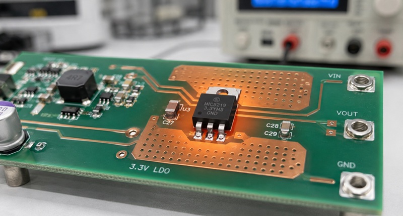
For many surface-mount LDOs, the PCB is the heatsink. The regulator package transfers heat into copper pads, copper pours, ground planes, and thermal vias. If the PCB copper area is too small, heat remains concentrated around the regulator and the package temperature rises quickly.
A common mistake is placing the LDO in a crowded corner of the board with only narrow traces connected to the power pins. Electrically, the circuit may still function. Thermally, the layout may fail because there is no effective heat spreading path.
Useful PCB thermal design methods include:
- Using larger copper pours connected to the regulator tab or exposed pad.
- Adding thermal vias to move heat into internal or bottom copper layers.
- Keeping heat-sensitive components away from the regulator package.
- Allowing airflow around the regulator when enclosure space permits.
- Using thicker copper for higher current or higher dissipation designs.
On small two-layer boards, even a modest increase in copper area can noticeably reduce regulator temperature. On four-layer boards, connecting the exposed pad to an internal ground plane through thermal vias often improves heat spreading. For compact industrial controllers, this layout work is often more important than selecting a slightly higher-rated LDO package.
Power Dissipation Before Package Selection
Package selection should not be based only on output current rating. Many LDO datasheets list high current capability, but that rating assumes favorable thermal conditions. A regulator rated for 1A may not safely deliver 1A if the input-output voltage difference is large and the PCB has poor thermal design.
Before selecting the final LDO package, engineers normally estimate worst-case power loss. This includes maximum input voltage, minimum output voltage, peak load current, high ambient temperature, and limited airflow inside the enclosure.
An LDO Power Dissipation Calculator fits naturally into this step because it helps evaluate the thermal load before package choice, copper area, and heatsink strategy are finalized.
| Package Type | Thermal Behavior | Design Note |
|---|---|---|
| SOT-23 | Limited heat dissipation | Best for low current and low voltage drop |
| SOT-223 | Moderate thermal capability | Needs enough copper area for practical heat spreading |
| DFN / QFN | Depends heavily on exposed pad layout | Thermal vias are usually important |
| TO-220 | Good with heatsink | Suitable for higher dissipation designs |
When an LDO Is Not the Right Thermal Choice
LDO regulators are useful when the design needs low noise, simple circuitry, or clean post-regulation after a switching stage. They are not always suitable when the voltage drop and load current create excessive heat.
An LDO may become a poor choice when:
- The input voltage is much higher than the output voltage.
- The load current is high.
- The PCB is small and has limited copper area.
- The enclosure has poor airflow.
- The ambient temperature is already high.
In these conditions, a switching regulator is usually more efficient. A common power architecture is to use a buck converter to step down the voltage first, then use an LDO to clean up ripple for sensitive analog, RF, sensor, or ADC power rails.
Practical LDO Thermal Design Checklist
Reliable LDO thermal design usually comes from checking several small details rather than relying on one large heatsink or one datasheet number.
- Calculate power dissipation before selecting the package.
- Check junction temperature under worst-case ambient conditions.
- Use enough copper area around the regulator package.
- Add thermal vias when using exposed-pad packages.
- Keep high-temperature components away from sensitive analog circuits.
- Consider a buck pre-regulator when voltage drop is too large.
- Verify real board temperature during prototype testing.
Reliable LDO thermal design depends on power dissipation, junction temperature, PCB copper area, package selection, and airflow. In compact power designs, thermal calculation should be completed before final PCB layout rather than after prototype failure.


