
 My Inquiry
 My Account


Open Collector vs Open Drain vs Push-Pull Outputs: Circuit Design Guide
Article Details
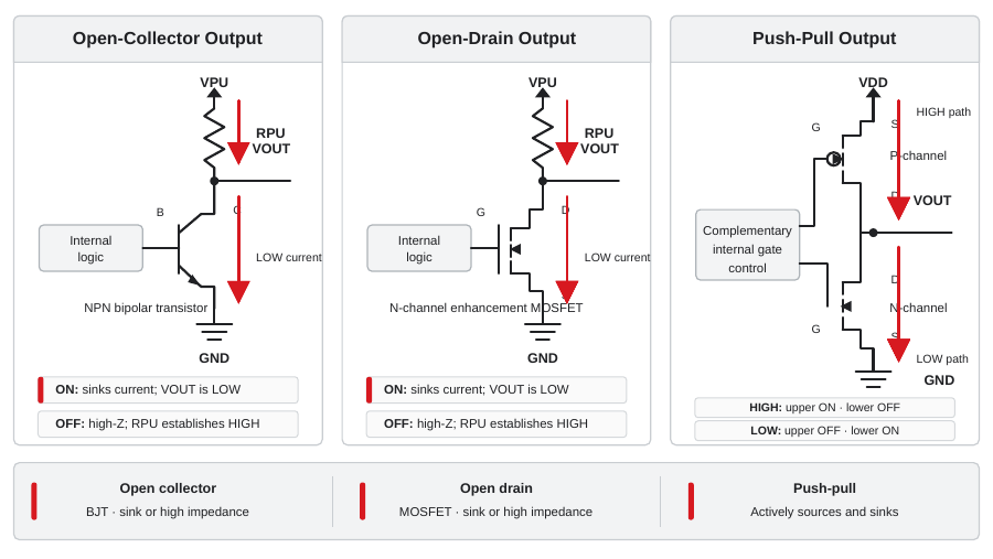
An open-collector output uses a bipolar transistor to pull a signal node LOW and releases the node for the HIGH state. An open-drain output performs the same external function with a MOSFET. Both need a pull-up resistor or another defined source of HIGH voltage. A push-pull output contains active pull-up and pull-down devices, so it drives both states directly.
Those structures impose different limits on sink current, output voltage, rise time, power sequencing and shared-bus connections. A signal that reaches the correct voltage on a static meter can still fail when leakage lowers its HIGH level, capacitance delays its rising edge, or an unpowered device clamps the pull-up rail.
Open Collector, Open Drain and Push-Pull at a Glance
| Output structure | Active devices at the pin | How LOW is produced | How HIGH is produced | Primary design constraint |
|---|---|---|---|---|
| Open collector | Usually one NPN bipolar transistor | The transistor saturates and sinks current through its collector | The transistor turns off; an external pull-up establishes the voltage | Collector voltage rating, VOL, sink current, leakage and passive rise time |
| Open drain | Usually one n-channel MOSFET | The MOSFET turns on and sinks current through its drain | The MOSFET turns off; an external pull-up establishes the voltage | Drain voltage rating, RDS(on) or VOL, leakage and passive rise time |
| Push-pull | Complementary upper and lower output devices | The lower device actively drives toward ground | The upper device actively drives toward the output supply | Source/sink current, loaded VOH/VOL, contention and voltage compatibility |
Open collector and open drain describe the transistor connected to the output node. Their external behavior is similar, while their semiconductor limits can differ substantially. An open-collector BJT is commonly specified by VCE, saturation voltage and collector current. An open-drain MOSFET may be specified by output voltage, VOL, RDS(on), leakage and sink current. The exact data-sheet table remains controlling.
How an Open-Collector Output Works
In the usual active-LOW circuit, the NPN emitter connects to ground and the collector connects to the output pin. Turning the transistor on creates a current path from the pull-up supply through RPU and the transistor to ground. The output voltage settles at the loaded VOL, often described as collector-emitter saturation voltage for a discrete transistor.
Turning the transistor off removes that pull-down path. The collector is then high impedance apart from leakage. The output has no internally driven HIGH state, so an omitted pull-up leaves the node undefined unless another circuit drives it.
How to Read the Open-Collector Symbol
A detailed open-collector symbol shows the output node connected to the collector of an NPN transistor with no upper transistor connected to the positive rail. Simplified logic symbols may identify the pin as OC, OD or open output in a pin table. An output bubble indicates logic polarity; it does not prove that the electrical stage is open collector. Confirm the topology in the functional diagram and output specifications.
How an Open-Drain Output Works
The corresponding MOS circuit uses an n-channel transistor with its source normally connected to ground and its drain connected to the output pin. A commanded LOW turns the MOSFET on. A commanded HIGH turns it off and places the output in its released state.
Microcontrollers often provide open-drain GPIO modes. With the output latch LOW, the pin sinks current; with the latch HIGH, the pin releases the bus. Register behavior varies by MCU, and some peripherals control the pad independently of the GPIO configuration. Microchip, for example, documents separate open-drain control in which the selected output becomes sink-only while standard mode can source and sink.
The pull-up can sometimes connect to a rail different from the device supply. Approval requires an explicit output-pin voltage range, suitable behavior when VCC is zero, and compatible receiver thresholds. The label "open drain" alone provides no voltage-tolerance guarantee.
Open Drain vs Push-Pull Output
A push-pull stage charges and discharges the load through active transistors. Its rising and falling edges can therefore be fast and comparatively symmetrical. The output HIGH remains dependent on source current and the guaranteed VOH specification; "active HIGH" does not mean an ideal connection to VCC.
An open-drain output discharges the node actively and charges it through RPU. The rising edge follows an RC curve, while the falling edge is set mainly by the transistor, interconnect inductance and load. This asymmetry is central to timing analysis.
| Design question | Open collector / open drain | Push-pull |
|---|---|---|
| External pull-up required? | Yes, unless another specified circuit establishes HIGH | No for normal enabled operation |
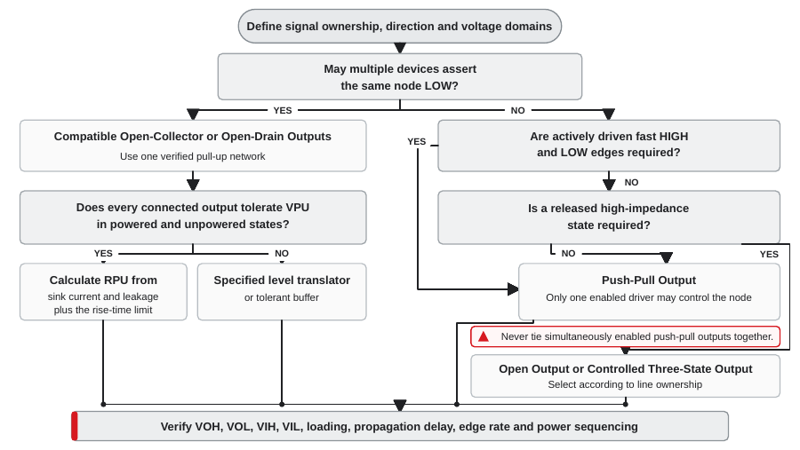
| Can several outputs share one node? | Yes when all outputs are compatible open outputs and one pull-up network satisfies every limit | Only with controlled tri-state ownership; two simultaneously enabled outputs can contend |
| Rising-edge behavior | Passive RC charging; often slower than the falling edge | Actively driven; normally faster for the same load |
| Static LOW-state current | Continuous current through the pull-up while LOW | Set mainly by the connected load and internal output stage |
| Different logic voltage at output? | Possible only within the output pin and power-state ratings | Normally tied to the driver's I/O supply; use a specified tolerant or translating device for other rails |
| Typical uses | I²C/SMBus, reset, interrupt, fault, power-good, comparators and shared alarm lines | Clocks, SPI, UART transmit, chip select and ordinary point-to-point GPIO |
Calculating the Pull-Up Resistor
A familiar 4.7 kΩ value is a starting point, not a universal selection. The acceptable range is bounded from below by LOW-state sink current and from above by HIGH-state leakage and rise time. Supply tolerance, resistor tolerance, temperature and the number of connected devices belong in the calculation.
Lower Resistance Limit: Sink Current and VOL
When the output transistor is on, it must carry the pull-up current plus any additional current entering the node from connected inputs. A conservative first pass assumes the LOW voltage can approach ground:
Use an IOL condition that guarantees an acceptable VOL, rather than the absolute maximum output current. Current above the data-sheet VOL test condition may produce a LOW voltage that the receiver no longer recognizes. The resistor's LOW-state dissipation should also be checked:
Upper Resistance Limit: HIGH-State Leakage
Released output transistors, receiver inputs, connectors and PCB contamination all contribute leakage. Use the worst-case direction that pulls the node away from VPU. The resulting HIGH voltage must remain above the receiver's guaranteed VIH(min):
For a shared node, ILEAK,total includes every released output and every receiver. Leakage can rise sharply at high temperature, so room-temperature typical values provide insufficient evidence.
Upper Resistance Limit: Rise Time
The released node charges through the pull-up resistor. For a single-pole approximation, the 10% to 90% rise time is:
CLOAD includes output capacitance, receiver input capacitance, PCB traces, connectors, cable and probe loading. Protocol specifications may define rise time between other voltage percentages; use the coefficient and thresholds required by that interface.
The final upper limit is the smaller of the DC leakage and timing results:
Worked Pull-Up Resistor Example
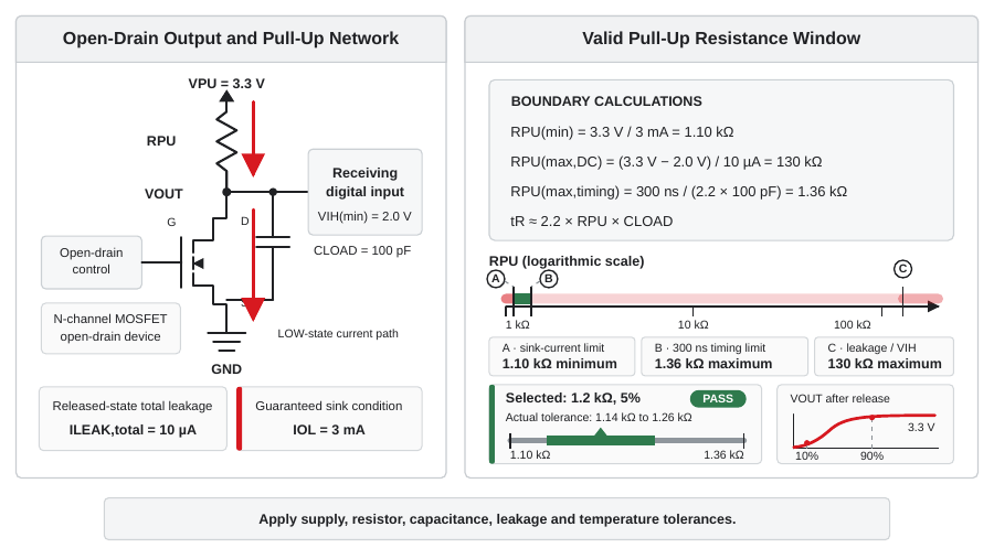
Consider an illustrative 3.3 V node with a receiver requiring VIH(min) = 2.0 V. The open-drain output guarantees the required VOL at IOL = 3 mA. Total worst-case released-state leakage is 10 µA, total capacitance is 100 pF, and the allowed 10% to 90% rise time is 300 ns.
| Constraint | Calculation | Result |
|---|---|---|
| Minimum resistance from sink current | 3.3 V / 3 mA | 1.10 kΩ |
| Maximum resistance from leakage | (3.3 V − 2.0 V) / 10 µA | 130 kΩ |
| Maximum resistance from rise time | 300 ns / (2.2 × 100 pF) | 1.36 kΩ |
| Usable calculated interval | 1.10 kΩ to 1.36 kΩ | Timing sets the upper boundary |
A nominal 1.2 kΩ, 5% resistor spans 1.14 kΩ to 1.26 kΩ. At 1.26 kΩ, the first-order rise time is about 277 ns and the 10 µA leakage drop is about 12.6 mV. At 1.14 kΩ, the idealized current with the node near ground is about 2.89 mA. Supply tolerance and all additional sink currents still need to be applied before approval.
The example shows why resistor selection can become narrow on a capacitive, fast node. Reducing capacitance, selecting an output with higher guaranteed sink current, relaxing the rise-time requirement or using a push-pull buffer may be more effective than forcing an unsuitable resistor value.
Wired-AND and Shared Open-Drain Lines
Compatible open-collector or open-drain outputs may connect to one node with a shared pull-up. Any conducting transistor pulls the node LOW; the node becomes HIGH only after every output releases it. With positive logic this behaves as wired-AND. With active-LOW signals the same physical connection is often described as wired-OR because any asserted fault forces the combined line LOW.
That connection requires more than matching topology labels:
- Every output pin must tolerate VPU in powered, startup, shutdown and unpowered states.
- The LOW-driving device must sink the pull-up current and any current from all receivers.
- Released-state leakage from every output must be added.
- The sum of device, trace and connector capacitance must meet the rise-time budget.
- Signal polarity must be defined so one device cannot unintentionally hold the system in reset or fault.
- Failures such as a shorted output or missing supply need a documented system response.
I²C and SMBus use open-drain signaling so multiple devices can acknowledge, arbitrate and hold a line LOW without two active output transistors driving opposite states. The bus pull-up calculation must follow the applicable protocol timing and capacitance limits; a generic GPIO calculation does not replace the bus specification.
Can an Open-Drain Output Translate Logic Voltage?
A suitable open-drain stage can produce a HIGH level referenced to the pull-up rail instead of the driver's supply. For example, a device powered at 5 V may feed a 3.3 V receiver through a 3.3 V pull-up, or a low-voltage open-drain buffer with a sufficiently rated output may pull up to a higher logic rail.
Four conditions decide whether that connection is valid:
- Output-pin voltage rating: VPU(max) must remain inside the recommended operating range for the open output, not merely below an absolute maximum.
- Receiver thresholds and stress limits: the resulting HIGH and LOW levels must satisfy VIH, VIL and the normal input-voltage range.
- Partial-power-down behavior: the output must permit the pull-up voltage while its own VCC is zero or ramping. Look for IOFF, fail-safe, powered-off protection or an equivalent explicit specification.
- Direction: one open-drain buffer normally translates in one signal direction. A bidirectional open-drain bus requires a topology specified for bidirectional operation.
Some pins contain a diode or clamp to VCC. A higher pull-up can then inject current into the supply, raise an unpowered rail or exceed the pin rating. The 3.3 V to 5 V Logic Level Shifter Guide covers receiver stress, direction and dedicated translator choices in more detail.
Where These Output Types Are Used
| Application | Common topology | Reason for the choice | Checks that commonly decide the design |
|---|---|---|---|
| Voltage comparator | Open collector, open drain or push-pull | Open outputs support an independent logic pull-up; push-pull provides active edges | Output polarity, VOL, pull-up range, response time and input common-mode limits |
| I²C / SMBus | Open drain | Multiple devices can pull the shared clock and data lines LOW | Bus capacitance, protocol rise time, sink current, level translation and stuck-bus behavior |
| Reset, fault and power-good | Frequently open drain or open collector | Several supervisors can share an active-LOW status line | Startup state, release delay, leakage, pull-up availability and fail-safe behavior |
| Interrupt line | Open drain when shared; push-pull when point-to-point | A shared active-LOW interrupt can identify that at least one source needs service | Firmware servicing, deassertion behavior, edge/level detection and line rise time |
| SPI clock, data output or chip select | Normally push-pull | Fast actively driven edges suit fixed-direction point-to-point signaling | Voltage levels, edge rate, ringing, source damping and tri-state bus ownership |
| GPIO strap or enable | Depends on required default and ownership | Open drain supports safe override; push-pull supports speed and direct drive | Boot state, internal pulls, external resistance, leakage and power sequencing |
The Comparator Circuit and LM393 Guide shows how an open-collector comparator interfaces with a 3.3 V microcontroller. For family-level threshold calculations, the TTL vs CMOS Logic Levels Guide explains the VOH, VOL, VIH and VIL comparisons.
Common Open-Collector and Open-Drain Failures
| Observed symptom | Likely electrical cause | Verification or correction |
|---|---|---|
| Output never goes HIGH | Missing pull-up, a device continuously pulling LOW, reversed logic polarity or an unpowered-device clamp | Disconnect loads in a controlled sequence; measure resistance to ground and inspect each device's state |
| HIGH voltage is too low | RPU is too large for total leakage, or the pull-up supply is incorrect | Calculate VOH(min) from worst-case leakage and compare it with receiver VIH(min) |
| LOW voltage is too high | RPU is too small, sink current exceeds the guaranteed condition, or too many loads source current into the node | Measure current and VOL at the pin; increase resistance or select a stronger rated output |
| Rising edge violates timing | Pull-up resistance or total capacitance is excessive | Measure at the receiver, calculate the RC limit and reduce RPU only within the sink-current budget |
| Device warms while the line is LOW | Continuous pull-up current exceeds the output or package power budget | Calculate current, duty cycle and resistor/output dissipation across supply tolerance |
| Board powers partially through a signal pin | Pull-up remains active while the open-drain device or receiver supply is off | Check IOFF and powered-off pin limits; change sequencing or add a specified translator/buffer |
| Two outputs fail after a firmware change | Push-pull pins were tied together and drove opposite levels | Use controlled tri-state ownership or compatible open outputs; never rely on software timing alone for unsafe contention |
Output-Interface Design Checklist
- Confirm open collector, open drain, push-pull or three-state operation from the exact data sheet.
- Record the allowed output voltage for every supply state, including VCC = 0 V.
- Compare guaranteed VOL and VOH with receiver VIL and VIH.
- Add leakage from every released output, receiver and protection network.
- Calculate the minimum pull-up resistance from guaranteed sink performance.
- Calculate both maximum resistance limits: HIGH-state leakage and rise time.
- Apply pull-up supply tolerance, resistor tolerance, capacitance tolerance and temperature.
- Check static LOW-state power and expected duty cycle.
- Verify that every output sharing a node is electrically compatible and uses the intended polarity.
- Capture startup, shutdown and fault behavior at the receiving pin.
- Measure rise time with realistic board, connector, cable and probe capacitance.
- Recheck the circuit when changing manufacturer, logic family, package or orderable suffix.
A robust open-output interface has a documented resistor interval rather than a habitual resistor value. The approved design shows positive logic margins, an acceptable edge at the receiver, safe sink current and defined behavior while each rail powers up or down.
Technical References
- Analog Devices - Open-Drain and Open-Collector Definition
- Texas Instruments - Choosing an Appropriate Pull-Up/Pull-Down Resistor for Open-Drain Outputs
- Texas Instruments - Applications of an Open-Drain Hex Buffer
- Analog Devices - Choosing Supervisor Outputs
- Microchip Technology - Open-Drain Control
Frequently Asked Questions
What is an open-collector output?
An open-collector output exposes the collector of a bipolar output transistor. The transistor actively sinks current for LOW and becomes high impedance when released. An external pull-up resistor normally creates the HIGH state.
What is the difference between open collector and open drain?
Open collector normally uses a bipolar transistor, while open drain uses a MOSFET. Both commonly pull LOW and release the output for HIGH. Their voltage, leakage, sink-current and power-off ratings depend on the exact device.
Why does an open-drain output need a pull-up resistor?
The output transistor can pull the node LOW but cannot actively source the HIGH state. The pull-up resistor establishes HIGH when the transistor is off and limits current when the transistor pulls LOW.
How is an open-drain pull-up resistor calculated?
The minimum resistance is set by guaranteed LOW-state sink current and VOL. The maximum resistance is set by released-state leakage and permitted rise time. Supply, resistor, capacitance and temperature tolerances must remain inside the calculated interval.
What is the difference between open drain and push-pull?
An open-drain output actively drives LOW and uses an external pull-up for HIGH. A push-pull output actively drives both HIGH and LOW, giving faster edges but preventing direct connection of multiple enabled outputs that may select opposite states.
Can open-collector outputs be connected together?
Yes, when every connected output is a compatible open type and all pins tolerate the pull-up voltage. The shared line is LOW when any output conducts and HIGH only when every output releases it.
Can an open-drain output be pulled up to a different voltage?
Sometimes. The pull-up voltage must remain within the output pin's recommended rating, the receiver must accept both logic levels, and the circuit must permit the voltage during startup, shutdown and unpowered operation.
Is every open-drain output 5 V tolerant?
No. Open-drain describes the output structure, while 5 V tolerance is a separate pin rating. Some low-voltage outputs contain clamps or have maximum voltages only slightly above their own supply.
Why is an open-drain rising edge slower than its falling edge?
The output transistor actively discharges the node for a falling edge. After release, the pull-up resistor charges total node capacitance exponentially, producing an RC-limited rising edge.
Can a push-pull output be used on an I²C bus?
Standard I²C signaling requires devices to release the line and allow other devices to pull it LOW. A push-pull HIGH can contend with another device's LOW. Use the peripheral mode and pin configuration specified for I²C.
Selecting and Sourcing Output-Interface Components
Choosing an open-collector comparator, open-drain buffer, logic gate or level translator requires the exact output topology, voltage range, package, temperature grade and orderable suffix. Search the Aetrix Electronics component catalog or submit the required part numbers, quantities and application constraints for sourcing review.


