
 My Inquiry
 My Account


TTL vs CMOS Logic Levels: 74HC and 74HCT Compatibility Explained
Article Details
TTL and CMOS describe two logic technologies with different input behavior, output drive, supply requirements and power consumption. A valid HIGH or LOW depends on guaranteed voltage limits at the driver and receiver; the family name alone does not establish compatibility.
The distinction becomes especially useful when choosing between 74HC and 74HCT devices. Both are CMOS families. A 74HC input uses CMOS-level thresholds, while a 74HCT input uses thresholds intended for 5 V TTL signals. Their outputs remain CMOS push-pull stages. The single letter T therefore changes the input interface without turning the device into bipolar TTL.
TTL vs CMOS at a Glance
| Design characteristic | TTL | CMOS | Engineering consequence |
|---|---|---|---|
| Basic technology | Bipolar junction transistors; classic 74xx and 74LS are common examples | Complementary MOSFET input and output structures; 74HC and 74HCT are common examples | Technology affects input current, output drive, static power and switching behavior. |
| Typical supply context | Legacy TTL families normally operate near 5 V; the permitted range is family- and part-specific | Supply range varies widely by family; a common 74HC implementation spans 2.0 V to 6.0 V, while HCT commonly requires 4.5 V to 5.5 V | CMOS does not automatically mean 3.3 V operation. HCT usually belongs to a 5 V rail. |
| 5 V input thresholds | Common TTL reference limits are VIH(min) = 2.0 V and VIL(max) = 0.8 V | HC thresholds track VCC; HCT uses TTL-compatible thresholds | A TTL HIGH can satisfy HCT and still fall below the guaranteed HIGH threshold of 5 V HC. |
| Input loading | Input current is directional and materially affects DC fan-out, especially in the LOW state | Very small DC leakage; input capacitance often sets the practical fan-out at speed | TTL fan-out is frequently current-limited. CMOS fan-out may be edge-rate- or delay-limited. |
| Output drive | Classic TTL outputs usually sink more current than they source | Push-pull CMOS outputs drive toward both rails, with guaranteed voltage tied to stated load current | Source and sink limits must be checked separately for the exact device. |
| Power behavior | Consumes static supply current even without switching; consumption depends on family and logic state | Low static current with valid rail-level inputs; switching power rises with capacitance, voltage and frequency | Slow or mid-rail CMOS inputs can create extra current and unstable operation. |
TTL is a broad historical category rather than one fixed electrical specification. Standard TTL, Schottky TTL, low-power Schottky TTL and later bipolar families have different output currents, delays and supply currents. CMOS also includes many families: CD4000, HC, HCT, AHC, AHCT, AC, ACT, LVC, AUC and others. The letters following "74" carry electrical meaning.
How Logic-Level Compatibility Is Calculated
A receiver guarantees a LOW at or below VIL(max) and a HIGH at or above VIH(min). Voltage between those limits is undefined. A driver guarantees that its LOW will remain at or below VOL(max) and its HIGH will remain at or above VOH(min) while carrying the specified load current.
LOW-state noise margin = VIL(max, receiver) − VOL(max, driver)
Both margins must be positive at the applicable supply tolerance, temperature and output current. Typical switching thresholds and unloaded bench measurements cannot replace guaranteed minimum and maximum values.
The voltage check is only the first gate. The receiver's recommended input range must accept the driver's entire output swing. A 5 V output may have adequate HIGH and LOW logic margins for a 3.3 V receiver yet exceed that receiver's input rating. The 3.3 V to 5 V logic-level shifter guide covers the input-stress and translator-circuit checks in more detail.
What TTL Logic Levels Mean
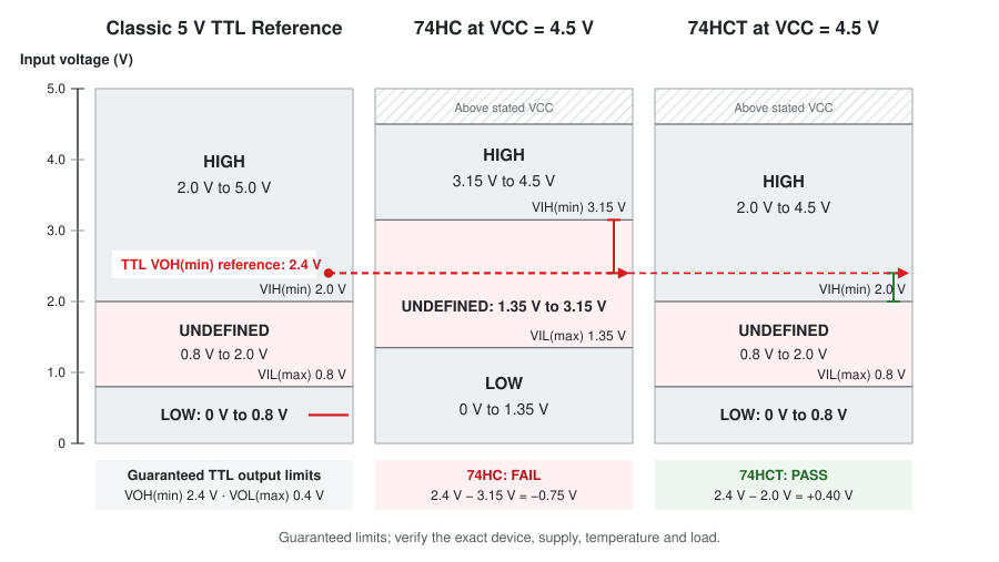
Transistor-transistor logic uses bipolar transistor input and output structures. The familiar 7400 and 74LS00 NAND gates are representative parts, although their electrical limits are not identical. TI specifies a 2.0 V minimum HIGH input and a 0.8 V maximum LOW input for the commercial 7400-class devices in its combined data sheet.
A standard SN7400-class output at its stated test current guarantees at least 2.4 V for HIGH and no more than 0.4 V for LOW. The HIGH output guarantee leaves 0.4 V of margin above a 2.0 V TTL input threshold; the LOW guarantee leaves 0.4 V below the 0.8 V input limit. A low-power Schottky part can have different output values and currents even though the familiar 2.0 V and 0.8 V input limits remain.
TTL output current is asymmetric
Classic TTL outputs generally sink more current than they source. For example, an SN74LS00 output is rated at a much larger LOW-state current than HIGH-state current under its recommended conditions. A load that works while the output is LOW may exceed the HIGH-state drive budget when the state reverses.
TTL inputs also draw state-dependent current. Their LOW input current has a larger magnitude than the HIGH input current, so the LOW-state fan-out calculation is often decisive. Leaving a TTL input open may make it drift toward a HIGH interpretation, but that behavior is not a valid bias method. Unused inputs require a defined connection consistent with the manufacturer's guidance.
What CMOS Logic Levels Mean
CMOS logic uses complementary p-channel and n-channel MOSFETs. An input near a supply rail turns one side of the input stage off and keeps static current low. During a transition, both devices can conduct briefly. Output switching also charges and discharges trace, package and receiver capacitance.
CMOS input thresholds often scale with supply voltage. In Nexperia's 74HC00 specification, the guaranteed limits at VCC = 4.5 V are:
- VIH(min) = 3.15 V
- VIL(max) = 1.35 V
Those values correspond to 0.7 × VCC and 0.3 × VCC. At VCC = 2.0 V, the same family uses different absolute thresholds. "CMOS level" therefore cannot be reduced to one universal pair of voltages.
Slow and floating CMOS inputs
A floating CMOS input can settle in the undefined region, increase supply current and oscillate in response to coupled noise. Every unused input needs a defined HIGH or LOW unless the exact device provides a bus-hold or other specified bias function. Outputs should not be tied directly to a supply rail merely because they are unused.
Rise and fall time also have data-sheet limits. A slow ramp holds the input stage in its linear region longer and can cause extra current, multiple output transitions or downstream timing errors. A Schmitt-trigger input is the usual choice for a deliberately slow or noisy signal; ordinary HC and HCT inputs should receive clean edges within their specified transition-rate limits.
74HC vs 74HCT: The Difference Is at the Input
74HC and 74HCT devices with the same function number usually implement the same Boolean logic and often share a pinout. Their defining difference is the input stage:
| Parameter | 74HC00 example | 74HCT00 example | Design meaning |
|---|---|---|---|
| Technology | High-speed CMOS | High-speed CMOS with TTL-compatible inputs | HCT is still CMOS; the T identifies its TTL-level input interface. |
| Recommended VCC | 2.0 V to 6.0 V | 4.5 V to 5.5 V | HCT should not be treated as a general 3.3 V family. |
| VIH(min) | 3.15 V at VCC = 4.5 V | 2.0 V at VCC = 4.5 V to 5.5 V | A TTL-level or many 3.3 V HIGH outputs can satisfy HCT more easily. |
| VIL(max) | 1.35 V at VCC = 4.5 V | 0.8 V at VCC = 4.5 V to 5.5 V | HC allows a higher LOW input at this supply, while HCT follows the TTL LOW limit. |
| Output type | CMOS push-pull | CMOS push-pull | An HCT output still swings toward its own supply rails; it is not voltage-limited to TTL output levels. |
| Input held below VCC | May enter the transition region if below the HC HIGH limit | Recognized as HIGH above the specified HCT limit, with possible additional supply current | Check the HCT device's ΔICC specification when inputs remain at TTL-level HIGH voltages. |
The same distinction appears in functions such as 74HC04 versus 74HCT04 and 74HC595 versus 74HCT595. The 74HC595 pinout and timing guide shows how the input-family choice affects a practical serial interface while the shift-register function remains the same.
Worked TTL-to-HC and TTL-to-HCT Comparison
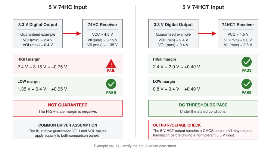
Consider a representative 5 V SN7400-class driver with VOH(min) = 2.4 V and VOL(max) = 0.4 V. Compare it with Nexperia 74HC00 and 74HCT00 receiver limits at the stated operating conditions.
| Connection | HIGH margin | LOW margin | Result |
|---|---|---|---|
| SN7400-class output to 74HC00 input at VCC = 4.5 V | 2.4 V − 3.15 V = −0.75 V | 1.35 V − 0.4 V = 0.95 V | Fails the guaranteed HIGH-state requirement even though the LOW state has margin. |
| SN7400-class output to 74HCT00 input at VCC = 4.5 V | 2.4 V − 2.0 V = 0.4 V | 0.8 V − 0.4 V = 0.4 V | Passes the DC threshold comparison at the stated loads and temperatures. |
The failed HC connection can appear functional on a prototype because an unloaded TTL output may rise above its guaranteed minimum and a particular HC input may switch below its guaranteed HIGH limit. Neither typical behavior provides production margin. HCT was created to close this specific interface gap.
Other solutions include a specified level translator or, in selected TTL interfaces, a pull-up resistor that raises the HIGH level. A pull-up changes output current, LOW-state dissipation and rise time. It belongs in the design only after checking the exact TTL output topology, resistor value, capacitance and timing.
Can 3.3 V Logic Drive 5 V HC or HCT?
A 3.3 V rail label does not prove the output HIGH voltage. The controlling specification is the driver's VOH(min) at the intended source current. Many 3.3 V GPIO outputs satisfy a 2.0 V HCT HIGH threshold with useful margin. The same output may fail the 3.15 V HIGH requirement of a 74HC input powered at 4.5 V.
A 74HC device powered from the same 3.3 V rail as the microcontroller is a different case. Its absolute threshold values fall with VCC, and a direct connection may have valid margin. That does not authorize the 74HC output to drive a non-tolerant lower-voltage input when the HC device is later moved to 5 V.
This distinction also appears when a 3.3 V controller drives a power shift register. The 74HC595 and TPIC6B595 comparison shows a device whose 5 V input threshold cannot be inferred from the "595" function name.
Can CMOS Drive TTL?
A 5 V CMOS output commonly provides ample voltage margin for a 5 V TTL input because its HIGH output approaches VCC and its LOW output approaches ground. Current remains part of the interface. A TTL receiver draws more LOW-state input current than a CMOS receiver, and one CMOS output may have to sink the combined current of several TTL inputs.
Calculate DC fan-out for both states:
LOW-state fan-out ≤ IOL(driver) ÷ |IIL(receiver)|
Use the smaller result and retain margin. The signs in data sheets indicate current direction; the magnitudes determine the count. Also add input capacitance, trace capacitance and connector loading. A connection can pass its DC fan-out calculation and still produce an edge too slow for the required clock or data timing.
Why a 5 V HCT Output Can Damage a 3.3 V Input
TTL-compatible input thresholds apply only to HCT inputs. A 5 V-powered HCT output is a CMOS output that can rise close to 5 V. Connecting it to a 3.3 V receiver is safe only when that receiving pin is explicitly 5 V tolerant or another authorized overvoltage interface is used.
Input clamp current, power-off behavior and injection-current limits require separate checks. A receiver powered down while its input remains HIGH can be back-powered through a protection structure. Look for IOFF, partial-power-down support or a stated input-voltage range that remains valid when VCC = 0 V. Absolute maximum ratings describe stress boundaries and should not be used as operating targets.
Power, Speed and Signal Integrity
Static and dynamic power
Classic TTL consumes supply current in a steady logic state. CMOS static current is much lower when inputs sit at valid rails, but switching power grows with load capacitance, supply voltage and transition frequency. A useful first-order relationship is:
The activity factor α represents how often a node switches. Package power also includes internal dissipation and any extra current caused by non-rail input levels. Use the device's ICC, CPD and ΔICC specifications when a reliable thermal or battery estimate is required.
Propagation delay and edge rate
Replacing a logic family changes more than DC thresholds. Propagation delay, output transition time and channel-to-channel skew can change the timing relationship between clock, data and enable signals. A faster family may also create more ringing on an unterminated trace. Series damping at the source, controlled return paths and local decoupling may be required even when the previous slower device worked without them.
Simultaneous switching
Several outputs changing together create transient current through VCC and ground inductance. Ground bounce reduces the effective LOW margin and supply droop reduces the effective HIGH margin. Place a ceramic bypass capacitor close to each logic package, keep return paths short and evaluate connector or cable inductance when many channels switch at once.
Logic-Family Selection Guide
| Interface requirement | Likely direction | Checks before selection |
|---|---|---|
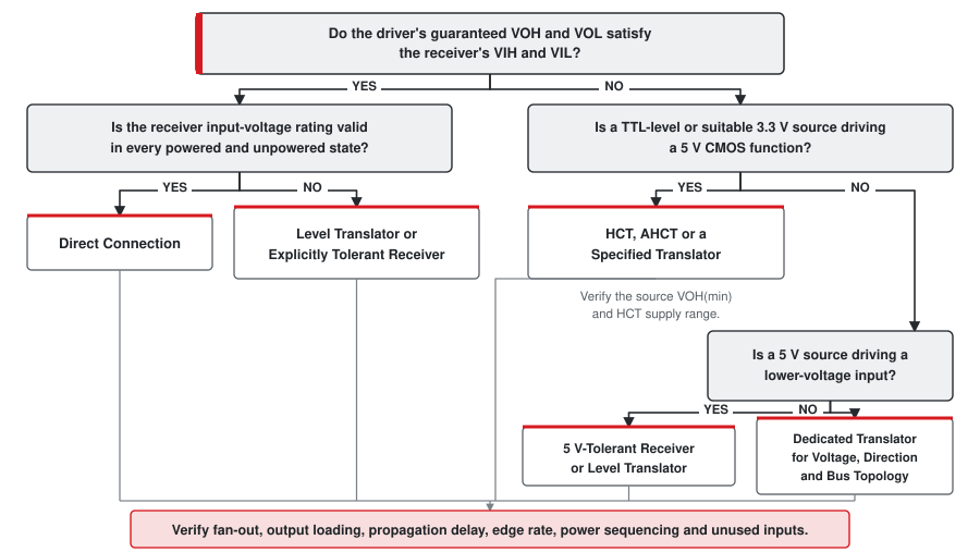
| 5 V TTL or 74LS output driving a 5 V CMOS function | Use the HCT or AHCT version of the required function when its speed, drive and package fit | Confirm VOH/VIH, VOL/VIL, ΔICC, fan-out and input edge rate. |
| 3.3 V MCU output driving 5 V logic | HCT/AHCT may provide a simple fixed-direction interface; a translator covers wider requirements | Use the MCU's guaranteed VOH(min); confirm the receiver supply range and HIGH threshold. |
| 5 V HC or HCT output driving 3.3 V logic | Use a 5 V-tolerant receiver or a suitable level shifter | Check the recommended input maximum, power-off behavior and timing. Do not rely on the absolute maximum. |
| Same-voltage modern CMOS connection | Direct connection is often suitable | Verify thresholds, output current, capacitive loading, edge rate and inactive power states. |
| Bidirectional bus across voltage domains | Use a translator designed for the bus topology | Separate open-drain buses such as I²C from push-pull buses; check direction control, pull-ups and contention. |
| Replacing a 74LS function with CMOS | HCT commonly offers the closest threshold match | Recheck pinout, unused inputs, output drive, edge speed, package, supply current and load behavior. |
Common Interface Failures
| Observed behavior | Likely cause | Engineering check |
|---|---|---|
| A 5 V HC input works on some boards and fails on others when driven from TTL | The HIGH level is inside the gap between the TTL output guarantee and HC input requirement | Calculate worst-case HIGH margin; change to HCT/AHCT or add a specified translator. |
| Supply current is unexpectedly high | An HCT input is held at a non-rail HIGH level, or a CMOS input is slow or floating | Measure every input at the IC pin and compare it with ΔICC and transition-rate conditions. |
| A replacement part causes ringing or double clocking | The new CMOS family has a faster output edge | Probe at the receiving pin, inspect the return path and consider source-series damping. |
| The interface fails only when one rail is off | Input current is back-powering an unpowered device | Check IOFF, input-voltage limits at VCC = 0 V and the complete power sequence. |
| One output cannot drive as many TTL inputs as expected | LOW-state input current or HIGH-state source current exceeds the fan-out budget | Calculate both DC fan-out limits and use the smaller value. |
| Unused gates switch or increase current | Inputs were left open | Tie each unused input to a valid logic level using the method permitted for that family and function. |
Replacing 74HC, 74HCT and TTL Parts
A shared function number does not make two devices electrically interchangeable. Before replacing a 74LS00 with a 74HCT00, or a 74HC04 with a 74HCT04, confirm:
- recommended supply-voltage range and tolerance;
- VIH, VIL, VOH and VOL at the actual loads;
- input and output current in both logic states;
- propagation delay, minimum pulse width and transition-rate limits;
- power-off input behavior and overvoltage tolerance;
- pinout, package dimensions, thermal limits and exposed-pad requirements;
- operating temperature, qualification and ESD ratings;
- manufacturer suffix, packing format and lifecycle status.
Aetrix lists devices from several logic families, including the 74HCT04S14-13 TTL-input-compatible CMOS inverter and the 74HC595D,118 CMOS shift register. The Nexperia product portfolio includes gates, buffers, latches and shift registers across multiple voltage and speed families. For a production replacement review, provide the complete manufacturer part number, package, supply rails, connected loads and quantity through the Aetrix RFQ page.
Technical References
- Nexperia 74HC00 / 74HCT00 product data sheet
- Nexperia HC/HCT User Guide
- Texas Instruments SN7400 / SN74LS00 family data sheet
- Texas Instruments SN54/74HCT CMOS Logic Family Applications and Restrictions
Frequently Asked Questions
What is the main difference between TTL and CMOS?
TTL uses bipolar transistor logic, while CMOS uses complementary MOSFETs. Their input currents, output drive, voltage thresholds, static power and switching behavior differ. Compatibility must be checked from guaranteed electrical limits.
What are standard TTL logic levels?
A common 5 V TTL reference uses VIL(max) = 0.8 V and VIH(min) = 2.0 V. Output guarantees vary by family and load; standard SN7400-class values include VOL(max) = 0.4 V and VOH(min) = 2.4 V under specified conditions.
What is the difference between 74HC and 74HCT?
Both families use CMOS technology. 74HC has CMOS-level inputs whose thresholds scale with supply voltage. 74HCT has TTL-compatible input thresholds and commonly operates from 4.5 V to 5.5 V. Their outputs are CMOS push-pull stages.
Is 74HCT a TTL device?
No. HCT is CMOS logic with an input stage designed to recognize TTL voltage levels. Its output characteristics and low static-current behavior remain those of a CMOS family.
Can a 3.3 V microcontroller drive a 5 V 74HCT input?
Often yes, provided the microcontroller's guaranteed VOH(min) exceeds the HCT VIH(min), its VOL(max) remains below VIL(max), and all input-voltage and power-state limits are satisfied. The rail value alone is not enough.
Can a 3.3 V microcontroller drive a 5 V 74HC input?
It may fail the guaranteed HIGH requirement. A 74HC input at VCC = 4.5 V can require 3.15 V, while the 3.3 V driver's guaranteed HIGH may be lower. Use the exact data sheets and calculate the worst-case margin.
Can a 5 V HCT output drive a 3.3 V input?
Only when the 3.3 V receiving pin is explicitly 5 V tolerant or a suitable level-shifting method is present. TTL-compatible thresholds apply to HCT inputs and do not limit an HCT output to 3.3 V.
Can 74HCT directly replace 74LS?
HCT often provides compatible input thresholds and matching logic functions, but replacement still requires checks for pinout, output current, timing, edge speed, unused inputs, package, power sequencing and qualification.
Why must unused CMOS inputs be connected?
A floating CMOS input can enter the undefined region, increase supply current and switch in response to noise. Tie it to a permitted logic level unless the device includes a specified bus-hold or bias function.
Which family uses less power, TTL or CMOS?
CMOS normally has much lower static power with valid rail-level inputs. Its dynamic power increases with switching activity, capacitance, supply voltage and frequency. A slow or mid-rail input can also add substantial current.


