What Is an FPGA? Architecture, FPGA Boards, Programming and Applications
Article Details
An FPGA is a programmable logic device that lets engineers create custom digital hardware after the chip has been manufactured. Unlike a fixed-function logic IC, an FPGA can be configured for different digital circuits, interfaces, control logic, signal processing paths, and acceleration tasks.
FPGA is a broad search term. Some users want the FPGA meaning, some want to understand FPGA boards, some are looking for FPGA programming, and others compare FPGA vs CPU, GPU, microcontroller, or ASIC. In electronics design, the most useful way to understand an FPGA is as reconfigurable hardware rather than ordinary software running on a processor.
This guide explains what an FPGA is, what FPGA stands for, how FPGA architecture works, how FPGA boards are used, how FPGA programming differs from software programming, how FPGA compares with MCU, CPU, GPU, and ASIC devices, and what engineers should check when selecting an FPGA device or FPGA development board.
Quick Answer: What Is an FPGA?
An FPGA, or Field-Programmable Gate Array, is a semiconductor device made of configurable logic blocks, programmable routing, memory blocks, DSP resources, clocking circuits, and I/O blocks. Engineers configure these resources to build custom digital hardware for a specific task.
| Item | Simple Explanation |
|---|---|
| Full name | Field-Programmable Gate Array |
| Main function | Implements custom digital hardware after manufacturing |
| Programmed with | Verilog, VHDL, SystemVerilog, block design tools, IP cores, and vendor toolchains |
| Best for | Parallel logic, low-latency I/O, custom interfaces, signal processing, protocol bridging, and hardware acceleration |
| Common vendors | AMD/Xilinx, Intel/Altera, Lattice, Microchip, Gowin |
What Does FPGA Mean?
FPGA stands for Field-Programmable Gate Array. Each word describes an important part of the device. The name means that the device can be configured in the field, after manufacturing, to implement hardware logic built from programmable resources.
| Term | Meaning | Why It Matters |
|---|---|---|
| Field | The device can be configured after manufacturing, often in the lab, factory, or deployed product. | The hardware function can be changed without making a new silicon chip. |
| Programmable | The internal logic and routing can be configured by a bitstream. | The same FPGA family can support many different circuit designs. |
| Gate Array | The device contains many configurable logic elements and routing resources. | Designers can build custom logic, state machines, interfaces, arithmetic paths, and processing blocks. |
The word programmable can be misleading for beginners. FPGA programming is not the same as writing a normal C or Python program for a CPU. In FPGA design, the engineer usually describes hardware behavior. The FPGA toolchain then maps that hardware description into logic blocks, routing, timing paths, and configuration data.
How Does an FPGA Work?
An FPGA works by configuring many small hardware resources inside the chip. These resources include lookup tables, flip-flops, routing switches, memory blocks, DSP blocks, clock management circuits, I/O banks, and sometimes high-speed serial transceivers or embedded processor cores.
A design is converted into a configuration file called a bitstream. When the FPGA is powered and configured, the bitstream defines how the internal logic blocks and routing connections behave. The result is a hardware circuit built inside the FPGA fabric.
| FPGA Resource | Function | Typical Use |
|---|---|---|
| Lookup table | Implements combinational logic functions | Boolean logic, multiplexers, small arithmetic functions |
| Flip-flop | Stores one bit of state | Registers, counters, state machines, pipelining |
| Routing matrix | Connects logic resources together | Signal paths between logic blocks, memory, DSP, and I/O |
| Block RAM | On-chip memory | Buffers, FIFOs, lookup tables, frame storage |
| DSP block | Dedicated arithmetic hardware | Filters, multiply-accumulate operations, signal processing |
| I/O bank | Connects FPGA logic to external pins | LVTTL, LVCMOS, LVDS, memory buses, control interfaces |
| Clock management | Generates, distributes, and conditions clock signals | PLL, MMCM, clock division, phase alignment |
| Transceiver | High-speed serial I/O block | PCIe, Ethernet, JESD204, high-speed communication links |

AMD describes FPGAs as flexible programmable devices used across requirements from low-cost software-defined technology to high-capacity networking, high bandwidth, and performance-per-watt applications. (AMD, FPGAs)
FPGA Internal Architecture Explained
FPGA architecture can be understood as a large grid of configurable hardware resources. A simple FPGA design may use only a small amount of logic and I/O. A larger design may use thousands of lookup tables, registers, memory blocks, clock networks, and DSP resources at the same time.
Configurable Logic Blocks
Configurable logic blocks are the main logic fabric of an FPGA. They contain lookup tables, flip-flops, and local routing. A lookup table can implement a small logic function, while flip-flops store state for synchronous designs.
These blocks are used to build counters, state machines, bus logic, arithmetic functions, custom control circuits, and many other digital structures. The FPGA toolchain decides how to map the design into available logic resources.
Programmable Routing
Routing resources connect logic blocks, memory blocks, DSP blocks, clock networks, and I/O pins. This routing is programmable, which means the same physical FPGA can support many different circuit structures.
Routing delay is a major part of FPGA timing. A design may be logically correct but still fail timing if signals cannot move through the routing fabric fast enough. This is one reason timing constraints and timing analysis are essential in FPGA projects.
Block RAM and Distributed Memory
Many FPGAs include block RAM for on-chip storage. Block RAM can be used for FIFOs, packet buffers, lookup tables, frame buffers, line buffers, and embedded processor memory. Some FPGA fabrics also support distributed memory built from logic resources.
Memory capacity matters when a design handles video lines, ADC samples, communication packets, or lookup tables. A small FPGA may have enough logic but not enough memory for a data-heavy application.
DSP Blocks
DSP blocks are dedicated arithmetic blocks optimized for multiplication, multiply-accumulate operations, filters, mixers, and signal-processing functions. They reduce logic usage and improve performance compared with building all arithmetic from general lookup tables.
Applications such as motor control, radar, software-defined radio, digital filtering, image processing, and edge acceleration may depend heavily on DSP block count and speed.
I/O Banks and Voltage Domains
FPGA I/O pins are usually grouped into banks. Each bank may require a specific I/O supply voltage. This matters when the FPGA must communicate with 1.8V, 2.5V, 3.3V, LVDS, or other signal standards.
I/O planning should happen early. A design can fail at the board level if the chosen FPGA package does not provide enough pins, the I/O banks cannot support the required voltages, or the board layout cannot route high-speed signals correctly.
Why Is an FPGA Different from a CPU?
A CPU executes software instructions in sequence, even when it has multiple cores. An FPGA creates custom hardware paths that can operate in parallel. This makes FPGAs useful when a system needs deterministic timing, low-latency I/O, or many operations running at the same time.
A CPU is easier to program and more flexible for general-purpose tasks. An FPGA is harder to design but can be better for custom data paths, hardware interfaces, real-time signal handling, and parallel processing. The difference is not only speed; it is the difference between executing instructions and building custom hardware behavior.
FPGA vs Microcontroller, CPU, GPU and ASIC
FPGA is often compared with microcontrollers, CPUs, GPUs, and ASICs. Each device type has a different design purpose. The best choice depends on performance, latency, power, cost, development time, and production volume.
| Device Type | Best At | Main Limitation | Typical Use |
|---|---|---|---|
| Microcontroller | Low-cost control, simple firmware, peripheral management | Limited parallel processing and high-speed custom I/O | Motor control, sensors, appliances, simple embedded systems |
| CPU | General-purpose software execution | Less deterministic for many low-latency hardware operations | Computers, servers, embedded Linux systems |
| GPU | Large-scale data parallel computation | Not ideal for every custom I/O or very low-latency control task | Graphics, AI training, image processing, parallel math |
| FPGA | Custom parallel hardware, low-latency I/O, reconfigurable logic | Development is more complex than ordinary software | Protocol bridging, data acquisition, video, communications, industrial control |
| ASIC | Highest efficiency for high-volume fixed functions | High development cost and no field reconfiguration | Mass-production chips, high-volume consumer and data-center silicon |
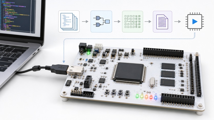
What Is an FPGA Board?
An FPGA board is a circuit board that contains an FPGA and the supporting components needed to power, configure, clock, connect, and test it. FPGA boards are used for learning, development, prototyping, verification, and sometimes production deployment.
A basic FPGA development board may include the FPGA device, configuration memory, voltage regulators, oscillator, USB or JTAG programming interface, user LEDs, switches, buttons, and I/O headers. More advanced boards may include DDR memory, Ethernet, PCIe, HDMI, ADC, DAC, FMC connectors, MIPI interfaces, or high-speed transceivers.
| Board Block | Purpose | Selection Point |
|---|---|---|
| FPGA device | Main programmable logic component | Logic cells, DSP blocks, RAM, I/O count, speed grade |
| Configuration memory | Stores the bitstream for FPGA startup | Memory size, interface type, boot mode |
| Power regulators | Provide core, auxiliary, and I/O voltages | Sequencing, current capacity, noise, efficiency |
| Oscillator or clock input | Provides timing reference | Frequency, jitter, clock routing, PLL compatibility |
| JTAG or USB programming | Loads and debugs FPGA configuration | Toolchain support and connector availability |
| External memory | Supports larger buffers and software systems | DDR type, capacity, bandwidth, layout quality |
| I/O connectors | Connects FPGA signals to other hardware | Voltage level, pin count, signal integrity, protection |
How Is an FPGA Programmed?
FPGA programming usually starts with a hardware description. Engineers use languages such as Verilog, VHDL, or SystemVerilog to describe the intended circuit behavior. Vendor tools then synthesize the design into FPGA logic resources.
FPGA programming can also use block design tools, IP cores, high-level synthesis, or graphical design flows. However, the final result is still hardware configuration, not ordinary software execution.
| Design Step | What Happens | Why It Matters |
|---|---|---|
| Design entry | Engineer writes HDL or builds a block design | Defines the hardware function |
| Simulation | Design behavior is tested before hardware programming | Finds logic errors early |
| Synthesis | HDL is converted into logic structures | Maps design intent into gates, registers, and resources |
| Place and route | Tool assigns logic to physical FPGA resources and connects routing | Determines timing, resource usage, and implementation quality |
| Timing analysis | Tool checks whether timing constraints are met | Critical for reliable hardware operation |
| Bitstream generation | Configuration file is created | Used to program the FPGA |
| Programming and debug | Bitstream is loaded into FPGA or configuration memory | Design is tested on real hardware |
The following video gives a beginner-friendly introduction to what an FPGA is, where it is used, and how FPGA design differs from ordinary programming.
FPGA Programming vs Software Programming
FPGA programming describes hardware structure and timing behavior. Software programming describes instructions that a processor executes. This difference affects how engineers think about performance, debugging, concurrency, and design verification.
| Topic | Software Programming | FPGA Design |
|---|---|---|
| Main concept | Instructions executed by a processor | Hardware logic configured inside the FPGA |
| Execution style | Mostly sequential, with threads or cores for parallelism | Many hardware blocks can run in parallel |
| Timing | Depends on processor speed, operating system, and instruction flow | Defined by clock domains, constraints, and hardware timing paths |
| Debugging | Software debugger, logs, breakpoints | Simulation, testbenches, logic analyzers, timing reports, on-chip debug |
| Output file | Executable or firmware image | Bitstream or configuration image |
Common FPGA Families and Brands
Several semiconductor manufacturers provide FPGA and programmable logic families. Brand names and part families matter because toolchains, IP cores, package options, I/O capabilities, lifecycle, and supply availability differ by vendor.
| Vendor | Common FPGA or Programmable Logic Families | Typical Positioning |
|---|---|---|
| AMD / Xilinx | Spartan, Artix, Kintex, Virtex, Zynq, UltraScale, Versal | Low-cost logic, embedded SoC, high-performance FPGA, adaptive SoC |
| Intel / Altera | MAX, Cyclone, Arria, Stratix, Agilex | CPLD, cost-optimized FPGA, mid-range FPGA, high-end programmable logic |
| Lattice | iCE40, MachXO, ECP, CrossLink | Low-power FPGA, small form factor, bridging, control, embedded vision |
| Microchip | IGLOO, SmartFusion, PolarFire | Low power, security-focused FPGA, SoC FPGA, industrial and aerospace use |
| Gowin | GW1N, GW2A, GW5A and related families | Cost-sensitive programmable logic and embedded applications |
Common FPGA-related part examples include XC7S6, XC7A35T, XC7Z020, EP4CE10, 10M08, LCMXO2, and LCMXO3.
What Is an FPGA Used For?
FPGAs are used when a system needs custom hardware behavior, many parallel operations, fast I/O response, or protocol-specific logic. They are common in engineering systems where a microcontroller or CPU cannot meet timing, bandwidth, or interface requirements alone.
| Application | Why FPGA Is Useful |
|---|---|
| Industrial control | Deterministic timing, custom I/O, parallel control loops |
| Motor control | Fast PWM, encoder processing, real-time protection logic |
| Data acquisition | High-speed ADC capture, buffering, triggering, custom filtering |
| Video processing | Parallel pixel pipelines, frame buffering, interface conversion |
| Communication systems | Protocol handling, packet processing, timing-sensitive data paths |
| Protocol bridging | Conversion between interfaces such as SPI, LVDS, MIPI, PCIe, Ethernet, or custom buses |
| Test equipment | Precise timing, pattern generation, signal capture, trigger logic |
| Edge AI and acceleration | Custom dataflow, low-latency inference, hardware acceleration |
How to Choose an FPGA
FPGA selection should start with the design requirements, not only the part number. The correct device depends on logic capacity, I/O count, memory, DSP requirements, speed, package, voltage, temperature grade, toolchain, lifecycle, and availability.
| Selection Parameter | What to Check |
|---|---|
| Logic cells or LUTs | Enough capacity for the intended logic design and future updates |
| Flip-flops | Registers needed for pipelining, counters, state machines, and control logic |
| Block RAM | Internal memory required for buffers, FIFOs, tables, and frame data |
| DSP blocks | Hardware multipliers and arithmetic blocks for signal processing |
| I/O count | Enough pins for interfaces, buses, control signals, and expansion |
| I/O voltage | Compatibility with external devices and I/O bank voltage planning |
| Transceivers | Required for PCIe, Ethernet, JESD204, and other high-speed serial links |
| Package | PCB routing difficulty, assembly process, thermal path, and board size |
| Power consumption | Core power, I/O power, dynamic switching power, and thermal design |
| Configuration method | Flash, SPI memory, JTAG, processor configuration, or secure boot options |
| Toolchain | Vendor software, simulation support, IP availability, and licensing |
| Lifecycle and supply | Availability, lead time, long-term support, and second-source strategy |
FPGA Board vs Bare FPGA Device
A beginner usually starts with an FPGA board. A board reduces the need to design power rails, clocks, programming circuits, memory, connectors, and PCB layout before learning the FPGA design flow. Production designs may use a bare FPGA device on a custom PCB.
| Option | Best For | Limitation |
|---|---|---|
| FPGA development board | Learning, prototyping, proof of concept, IP evaluation | May not match final size, cost, connector, or power requirements |
| Custom FPGA PCB | Production hardware, optimized form factor, custom I/O, final system integration | Requires power design, signal integrity, configuration, clocking, and layout expertise |
Common Mistakes When Using FPGAs
FPGA projects can fail when designers treat the FPGA like a microcontroller, ignore timing constraints, or underestimate the board-level requirements. FPGA design needs both digital logic knowledge and hardware implementation awareness.
- Thinking FPGA programming is the same as ordinary software programming.
- Writing HDL without simulation or testbenches.
- Ignoring timing constraints and assuming the design will automatically meet timing.
- Choosing an FPGA with too few LUTs, I/O pins, RAM blocks, or DSP blocks.
- Using the wrong I/O voltage for an external device.
- Forgetting that FPGA I/O banks often share voltage constraints.
- Ignoring power sequencing, rail current, and regulator noise requirements.
- Not planning configuration memory, JTAG access, or boot mode.
- Underestimating PCB routing difficulty for BGA packages and high-speed interfaces.
- Ignoring clocking, reset synchronization, and metastability in multi-clock designs.
- Assuming a development board design can be copied directly into production without review.
Quick Reference: FPGA Terms
| Term | Meaning |
|---|---|
| HDL | Hardware description language, such as Verilog or VHDL |
| Bitstream | Configuration file used to program the FPGA |
| LUT | Lookup table used to implement logic functions |
| BRAM | Block RAM inside the FPGA fabric |
| DSP slice | Dedicated arithmetic block for multiplication and signal processing |
| Timing closure | Process of ensuring the implemented design meets timing requirements |
| IP core | Reusable design block for functions such as memory controllers, interfaces, or processors |
| JTAG | Common interface for programming and debugging FPGA devices |
Frequently Asked Questions
What is FPGA in simple words?
An FPGA is a chip that can be configured to become custom digital hardware. Engineers use it to build logic circuits, interfaces, processors, filters, controllers, and other hardware functions after the chip is manufactured.
What does FPGA stand for?
FPGA stands for Field-Programmable Gate Array.
Is FPGA a microcontroller?
No. A microcontroller runs firmware instructions on a fixed processor core. An FPGA is configured to create custom hardware logic. Some FPGA SoC devices include processor cores, but the FPGA fabric itself is different from a microcontroller.
Is FPGA faster than CPU?
An FPGA is not always faster for every task. It can be faster or lower-latency for custom parallel hardware, streaming data paths, timing-sensitive I/O, and protocol-specific processing. A CPU is usually better for general-purpose software tasks.
What is an FPGA board?
An FPGA board is a circuit board that includes an FPGA plus supporting components such as power regulators, clock sources, configuration memory, programming interface, connectors, and sometimes external memory or communication ports.
What language is used for FPGA programming?
Common FPGA design languages include Verilog, VHDL, and SystemVerilog. Some flows also use high-level synthesis, block design tools, or vendor IP cores.
What is FPGA used for?
FPGAs are used for industrial control, data acquisition, video processing, communications, protocol bridging, motor control, test equipment, aerospace systems, and hardware acceleration.
What is the difference between FPGA and ASIC?
An FPGA is reconfigurable after manufacturing. An ASIC is a custom chip manufactured for a fixed function. ASICs can be more efficient in high-volume production, but they have higher development cost and cannot be reconfigured like an FPGA.
Is Xilinx an FPGA?
Xilinx is a major FPGA brand, now part of AMD. The term refers to FPGA and adaptive SoC products such as Spartan, Artix, Kintex, Virtex, Zynq, UltraScale, and Versal families.
Is Altera the same as Intel FPGA?
Altera was acquired by Intel. Many older FPGA products and references still use the Altera name, while newer branding is Intel FPGA.
An FPGA is a reconfigurable digital hardware device used when a system needs custom logic, parallel processing, low-latency I/O, or interface-specific control. It sits between fixed-function logic ICs, microcontrollers, CPUs, GPUs, and ASICs in the design space.
For engineering selection, the most important points are logic capacity, memory, DSP resources, I/O banks, voltage compatibility, clocking, configuration method, package, power, toolchain support, lifecycle, and supply availability. A good FPGA choice should match both the digital logic design and the board-level hardware requirements.