What Is a Logic Gate? Types, Truth Tables, Symbols and Applications
Article Details
A logic gate is a basic building block of digital electronics. It receives one or more binary inputs and produces one binary output according to a Boolean logic rule. Logic gates are used inside microcontrollers, processors, memory devices, programmable logic, digital control circuits, communication interfaces, and many other electronic systems.
In a digital circuit, binary values are represented by voltage levels. A logic 0 usually means a low voltage, and a logic 1 usually means a high voltage. The exact voltage range depends on the logic family, supply voltage, and device specification. This is why a logic gate is not only a theoretical Boolean function, but also a real electronic component with voltage thresholds, output drive limits, delay time, and package options.
This guide explains what a logic gate is, how logic gates work, the main types of logic gates, truth tables, universal logic gates, logic gate ICs, and practical applications in electronic circuits.
What Is a Logic Gate?
A logic gate is a digital circuit that performs a logical operation on binary inputs. The output depends on the input state and the function of the gate. For example, an AND gate outputs 1 only when all inputs are 1, while an OR gate outputs 1 when at least one input is 1.
Logic gates are called gates because they control whether a signal condition is allowed to produce an output. They can combine signals, invert signals, compare signals, enable or disable functions, and create decision logic inside a larger digital system.
At the circuit level, logic gates are usually built from transistors. At the component level, they may appear as logic ICs such as NAND gate ICs, inverter ICs, AND gate ICs, OR gate ICs, XOR gate ICs, or configurable logic devices.
| Term | Meaning in Digital Electronics |
|---|---|
| Logic 0 | A low-voltage state interpreted as binary 0. |
| Logic 1 | A high-voltage state interpreted as binary 1. |
| Input | A signal applied to the logic gate. |
| Output | The result produced by the logic gate. |
| Truth table | A table showing the output for every possible input combination. |
| Boolean logic | The mathematical system used to describe logic operations. |
How Logic Gates Work
Logic gates work by switching electronic devices inside the circuit. In CMOS logic, the switching action is usually performed by MOSFET transistors. Different transistor arrangements create different logic functions such as AND, OR, NOT, NAND, NOR, XOR, and XNOR.
In a real circuit, the input pins do not receive abstract numbers. They receive voltages. The logic IC interprets those voltages as low or high according to its input threshold. The output then drives another logic input, LED driver, transistor, microcontroller pin, latch, flip-flop, or other circuit block.
Practical logic gate behavior depends on more than the truth table. Supply voltage, input logic threshold, propagation delay, output current, package type, temperature range, and logic family all affect whether the device works correctly in a real design.
| Practical Parameter | Why It Matters |
|---|---|
| Supply voltage | The logic IC must support the circuit voltage, such as 1.8V, 3.3V, or 5V. |
| Input threshold | The input must recognize the driving signal correctly as logic low or logic high. |
| Output drive current | The output must be able to drive the connected load or next logic input. |
| Propagation delay | The output changes after a small delay when the input changes. |
| Package | The package must fit the PCB layout, assembly process, and size requirement. |
| Logic family | Different families such as 74HC, 74HCT, 74LVC, and 4000-series CMOS have different electrical behavior. |
The following video gives a beginner-friendly explanation of logic gates and truth tables before the article moves into gate types, universal gates, IC examples, and engineering design notes.
Basic Types of Logic Gates
The basic logic gates are AND, OR, and NOT. Other common gates include NAND, NOR, XOR, XNOR, and buffer gates. Each gate has a different Boolean function and a different output behavior.
| Logic Gate | Function | Output Is 1 When | Common Use |
|---|---|---|---|
| AND | Logical multiplication | All inputs are 1 | Enable logic, interlock control, condition checking |
| OR | Logical addition | At least one input is 1 | Combining request signals, error flags, wake signals |
| NOT | Inversion | Input is 0 | Signal inversion, polarity conversion |
| NAND | Inverted AND | Not all inputs are 1 | Universal logic, latch circuits, digital control |
| NOR | Inverted OR | All inputs are 0 | Universal logic, reset logic, enable control |
| XOR | Exclusive OR | Inputs are different | Parity checking, adders, comparison circuits |
| XNOR | Exclusive NOR | Inputs are the same | Equality detection, comparison logic |
| Buffer | Non-inverting signal transfer | Input is 1 | Signal restoration, drive-strength improvement |
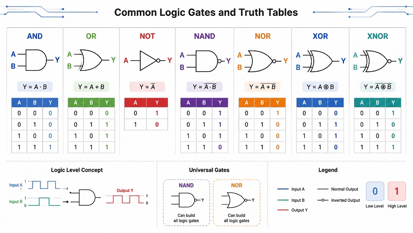
Logic Gate Truth Tables
A truth table shows every possible input combination and the corresponding output. For a two-input logic gate, there are four possible input combinations: 00, 01, 10, and 11. Truth tables are useful because they describe gate behavior without needing a full circuit diagram.
AND Gate Truth Table
| Input A | Input B | Output Y |
|---|---|---|
| 0 | 0 | 0 |
| 0 | 1 | 0 |
| 1 | 0 | 0 |
| 1 | 1 | 1 |
OR Gate Truth Table
| Input A | Input B | Output Y |
|---|---|---|
| 0 | 0 | 0 |
| 0 | 1 | 1 |
| 1 | 0 | 1 |
| 1 | 1 | 1 |
NOT Gate Truth Table
| Input A | Output Y |
|---|---|
| 0 | 1 |
| 1 | 0 |
NAND, NOR, XOR and XNOR Truth Table
| Input A | Input B | NAND | NOR | XOR | XNOR |
|---|---|---|---|---|---|
| 0 | 0 | 1 | 1 | 0 | 1 |
| 0 | 1 | 1 | 0 | 1 | 0 |
| 1 | 0 | 1 | 0 | 1 | 0 |
| 1 | 1 | 0 | 0 | 0 | 1 |
What Is an AND Logic Gate?
An AND gate outputs 1 only when all of its inputs are 1. If any input is 0, the output is 0. This makes the AND gate useful for circuits where several conditions must all be true before an output is allowed.
A common example is an enable circuit. If a power-good signal is 1 and a control-enable signal is 1, the AND gate output can activate the next stage. If either condition is missing, the output remains 0.
What Is an OR Logic Gate?
An OR gate outputs 1 when at least one input is 1. The output is 0 only when all inputs are 0. OR gates are often used to combine signals where any one condition should trigger the output.
For example, several fault signals can be connected through OR logic so that any single fault can activate a warning input. OR gates are also used in wake-up logic, interrupt logic, and request-signal combining.
What Is a NOT Logic Gate?
A NOT gate has one input and one output. It inverts the input. If the input is 0, the output is 1. If the input is 1, the output is 0. A NOT gate is also called an inverter.
Inverters are used when a signal polarity must be changed. For example, a circuit may need an active-low reset signal even though the controlling signal is active-high. An inverter can convert one polarity into the other.
What Is a Universal Logic Gate?
A universal logic gate is a gate that can be used to build all other basic logic functions. NAND and NOR are universal logic gates. With only NAND gates, it is possible to build NOT, AND, OR, NOR, XOR, and other logic functions. The same is true for NOR gates.
Universal gates are important in digital design because they show that complex logic can be built from a small number of repeated building blocks. This idea is used in logic education, IC design, programmable logic, and circuit optimization.
| Universal Gate | Why It Is Universal | Example Use |
|---|---|---|
| NAND | NAND gates can be connected to create NOT, AND, OR, and other gates. | General-purpose digital logic, latches, control circuits |
| NOR | NOR gates can also create all basic Boolean functions. | Reset logic, latch circuits, compact logic functions |
Logic Gate Symbols
Logic gate symbols provide a standard way to represent digital logic functions in schematics. A gate symbol shows the input side, output side, and inversion bubbles when a signal is inverted. For example, a NAND gate is usually drawn like an AND gate with a small bubble at the output. A NOR gate is usually drawn like an OR gate with a small bubble at the output.
Symbols are useful for reading circuit diagrams, but the truth table is the most direct way to confirm what a gate does. When learning logic gates, it is useful to compare the symbol, Boolean expression, and truth table together.
| Gate | Common Boolean Expression | Simple Meaning |
|---|---|---|
| AND | Y = A · B | Y is 1 when A and B are both 1. |
| OR | Y = A + B | Y is 1 when A or B is 1. |
| NOT | Y = A̅ | Y is the opposite of A. |
| NAND | Y = A · B | Y is the inverted result of AND. |
| NOR | Y = A + B | Y is the inverted result of OR. |
| XOR | Y = A ⊕ B | Y is 1 when A and B are different. |
Logic Gate ICs and Logic Families
A logic gate can be implemented inside a large digital chip, but it can also be purchased as a separate logic IC. These ICs are useful when a design needs a small amount of digital logic without using a microcontroller, FPGA, or larger programmable device.
Common logic families include 74HC, 74HCT, 74LVC, 74AUP, 74LS, and 4000-series CMOS. Different families support different voltage ranges, speed, drive strength, input thresholds, power consumption, and package options.
Texas Instruments organizes logic gates by categories such as AND gates, NAND gates, NOR gates, OR gates, XOR gates, XNOR gates, voltage-translating gates, and other logic functions, with selection options such as voltage range and package type. (Texas Instruments, Logic Gates)
| Example Logic IC | Gate Type | Typical Function |
|---|---|---|
| 74HC00 | NAND gate | Quad 2-input NAND gate logic |
| 74HC04 | NOT gate / inverter | Hex inverter for signal polarity conversion |
| 74HC08 | AND gate | Quad 2-input AND gate logic |
| 74HC32 | OR gate | Quad 2-input OR gate logic |
| 74HC86 | XOR gate | Quad 2-input XOR gate logic |
| CD4011 | NAND gate | CMOS NAND gate used in 4000-series logic designs |
| CD4071 | OR gate | CMOS OR gate used in 4000-series logic designs |
Logic Gates in Real Electronic Applications
Logic gates are used in both simple and complex electronic systems. In a simple board, a gate may combine two control signals. In a complex chip, millions or billions of transistor-level gates may form registers, adders, decoders, memory interfaces, processors, and communication logic.
| Application | How Logic Gates Are Used |
|---|---|
| Enable and disable control | Allows a circuit block to operate only when the required conditions are true. |
| Signal inversion | Converts active-high signals to active-low signals, or the reverse. |
| Reset logic | Combines multiple reset sources or creates correct reset polarity. |
| Chip select logic | Selects a memory device, peripheral, or digital interface. |
| Interlock circuits | Requires multiple conditions to be valid before an output is activated. |
| Parity and comparison | XOR and XNOR gates help detect difference, equality, and parity. |
| Address decoding | Logic gates help map address lines to chip select signals. |
| FPGA and ASIC design | Logic gates form the basis of larger digital logic structures. |
Logic Gates vs Logic ICs vs Digital Circuits
The terms logic gate, logic IC, and digital circuit are related, but they do not mean exactly the same thing.
| Term | Meaning | Example |
|---|---|---|
| Logic gate | A Boolean function such as AND, OR, NOT, NAND, or XOR. | An AND gate function inside a circuit. |
| Logic IC | A physical integrated circuit containing one or more logic gates. | 74HC00, 74HC04, 74HC08, 74HC32. |
| Digital circuit | A larger circuit built from gates, registers, clocks, memories, or controllers. | A counter, decoder, processor, FPGA, or control board. |
A single logic IC may contain one gate, two gates, four gates, six inverters, or a more complex combination. A digital system may contain many logic ICs or may integrate the logic internally inside an MCU, FPGA, CPLD, or ASIC.
Common Mistakes When Using Logic Gates
Logic gates look simple in truth tables, but real circuit designs can fail if electrical details are ignored. The most common problems involve floating inputs, incompatible voltage levels, weak output drive, missing decoupling, or incorrect interpretation of active-low signals.
- Leaving CMOS logic inputs floating instead of tying them to a defined logic level.
- Mixing 5V and 3.3V logic without checking input tolerance and output levels.
- Using 74HC and 74HCT devices interchangeably without checking threshold requirements.
- Ignoring propagation delay in timing-sensitive circuits.
- Driving loads that exceed the output current rating of the logic IC.
- Forgetting decoupling capacitors near the logic IC supply pins.
- Misreading active-low outputs or inversion bubbles in a schematic.
- Connecting unused inputs incorrectly or leaving unused gates in unstable states.
- Assuming similar part numbers are pin-compatible without checking the datasheet.
- Using a package that is difficult to assemble, test, or source.
Quick Reference: Logic Gate Selection
| Selection Point | What to Check |
|---|---|
| Gate function | AND, OR, NOT, NAND, NOR, XOR, XNOR, buffer, or configurable logic. |
| Number of channels | Single gate, dual gate, quad gate, hex inverter, or multi-function device. |
| Supply voltage | Confirm that the IC supports the board voltage. |
| Logic threshold | Check whether the input thresholds match the driving device. |
| Output drive | Confirm current rating and fanout requirement. |
| Speed | Check propagation delay and switching performance. |
| Package | Select a package suitable for PCB area, assembly, and availability. |
| Temperature range | Choose commercial, industrial, automotive, or extended temperature grade as required. |
Frequently Asked Questions
What is a logic gate?
A logic gate is a digital circuit that performs a Boolean operation on one or more binary inputs and produces one binary output.
What are the basic logic gates?
The basic logic gates are AND, OR, and NOT. Other common gates include NAND, NOR, XOR, XNOR, and buffer gates.
What is an AND logic gate?
An AND gate outputs 1 only when all inputs are 1. If any input is 0, the output is 0.
What is an OR logic gate?
An OR gate outputs 1 when at least one input is 1. The output is 0 only when all inputs are 0.
What is a NOT logic gate?
A NOT gate inverts the input. If the input is 0, the output is 1. If the input is 1, the output is 0.
What is a universal logic gate?
A universal logic gate can be used to build all other basic logic functions. NAND and NOR gates are universal logic gates.
Why are truth tables important?
Truth tables show the output of a logic gate for every possible input combination, making it easier to understand and verify digital logic behavior.
Are logic gates physical components?
A logic gate is a function, but it can be implemented as a physical logic IC, inside a microcontroller, inside an FPGA, or as transistor-level circuitry in a larger chip.
A logic gate is one of the most important concepts in digital electronics. It converts binary input conditions into a binary output according to a Boolean rule. Simple gates such as AND, OR, and NOT form the basis of more complex logic, while NAND and NOR gates can be used as universal building blocks.
In real electronic design, logic gates must be selected by both logic function and electrical specification. Supply voltage, input threshold, output drive, propagation delay, package, and logic family all matter. A truth table explains what the gate does, but the datasheet explains whether the gate will work correctly in the circuit.