
 My Inquiry
 My Account


NXP Semiconductors 74HC00D/AUJ
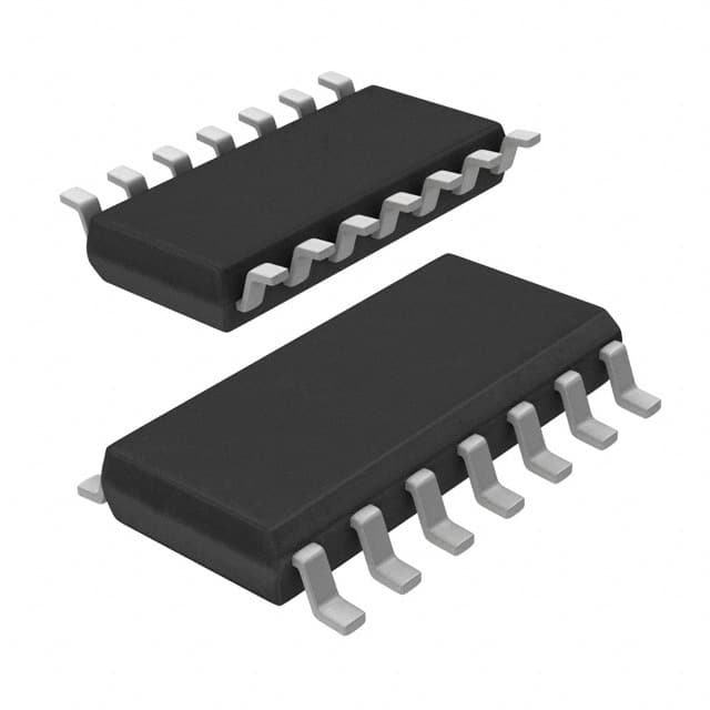
- Part No.:
- 74HC00D/AUJ
- Manufacturer:
- NXP Semiconductors
- Category:
- Gates and Inverters
- Package:
- 14-SOIC (0.154", 3.90mm Width)
- Datasheet:
-
 74HC00D/AUJ.pdf
- Description:
- IC GATE NAND 4CH 2-INP 14SO
- Quantity:
- Payment:

- Shipping:

Inventory:1,556
Please send an inquiry. Send us your inquiry, and we will respond immediately.
Product details
Overview
74HC00D/AUJ from NXP USA Inc. is a quad 2-input NAND gate designed for general-purpose CMOS logic, signal inversion, gate-level control, combinational logic, address qualification, timing logic, and embedded digital systems. The device integrates four independent 2-input NAND gates in a 14-lead SOIC package, allowing designers to implement multiple logic functions with a single standard logic IC.
As part of the 74HC00 high-speed CMOS logic family, 74HC00D/AUJ combines a 2.0V to 6.0V supply range, CMOS input levels, low power dissipation, high noise immunity, input clamp diodes, and standard NAND-gate functionality for flexible board-level logic integration. For engineers reviewing the 74HC00D/AUJ datasheet, 74HC00D/AUJ pinout, 74HC00D/AUJ application, or 74HC00D/AUJ equivalent, this device is widely used in digital logic gates, signal conditioning, address decoding, enable logic, oscillator circuits, latch structures, embedded controllers, industrial boards, and general-purpose CMOS logic designs.
Technical Context
In digital logic systems, 74HC00D/AUJ provides four independent NAND gates. Each gate outputs LOW only when both inputs are HIGH; if either input is LOW, the output remains HIGH. Because NAND gates are universal logic elements, the device can be used to build inverters, AND gates, OR gates, latches, gated control functions, and more complex combinational logic.
The HC version uses CMOS input thresholds and operates across a 2.0V to 6.0V supply range, making it suitable for CMOS-level 3.3V and 5V systems. Compared with HCT versions, the HC device is not intended for TTL-level input thresholds; designers should verify that the driving circuit provides valid CMOS HIGH and LOW levels for the selected VCC.
The device includes input clamp diodes, allowing inputs to be interfaced to voltages above VCC through current-limiting resistors. This can simplify certain mixed-voltage interface cases, but input clamp current and absolute maximum ratings must still be respected during circuit design.
Key Specifications
| Parameter | Value and Actual Design Meaning |
|---|---|
| Device Type | Quad 2-input NAND gate for standard CMOS logic implementation. |
| Logic Family | 74HC high-speed CMOS logic with CMOS input-level compatibility. |
| Gate Count | Four independent 2-input NAND gates in one package. |
| Logic Function | Each output is LOW only when both corresponding inputs are HIGH. |
| Supply Voltage | 2.0V to 6.0V recommended operating range for 74HC00 operation. |
| Input Levels | CMOS input levels for 74HC00 operation. |
| Propagation Delay | 9ns typical at VCC = 4.5V and CL = 50pF, supporting fast board-level logic switching. |
| Input Capacitance | 3.5pF typical, supporting standard CMOS logic input loading. |
| Power Dissipation Capacitance | 22pF typical per package for estimating dynamic power dissipation. |
| Output Current Rating | ±25mA absolute maximum output current rating per output pin; practical drive should follow datasheet operating conditions. |
| Input Protection | Inputs include clamp diodes for current-limited interfacing to voltages above VCC. |
| ESD Protection | HBM class 2 above 2000V and CDM class C3 above 1000V. |
| Latch-Up Performance | Exceeds 100mA per JESD 78 Class II Level B. |
| Operating Temperature | -40°C to +125°C operating range for the 74HC00D package option. |
| Package | SO14 plastic small outline package, body width 3.9mm, SOT108-1. |
Pinout & Package
The 74HC00D/AUJ pinout uses a 14-lead SOIC package with four independent NAND gate sections. Gate 1 uses inputs 1A and 1B with output 1Y; gate 2 uses 2A and 2B with output 2Y; gate 3 uses 3A and 3B with output 3Y; and gate 4 uses 4A and 4B with output 4Y. Pin 7 is GND and pin 14 is VCC.
For PCB implementation, VCC should be bypassed close to the package, unused inputs should be tied to VCC or GND, and outputs should not be shorted together unless the logic design specifically supports that condition. Since NAND gates are often used in gating and edge-sensitive logic, clean input transitions and valid CMOS threshold margins should be maintained.
| Pin / Function | PCB Design and Circuit Role |
|---|---|
| Pin 1 / 1A | Input A of NAND gate 1. |
| Pin 2 / 1B | Input B of NAND gate 1. |
| Pin 3 / 1Y | Output of NAND gate 1. |
| Pin 4 / 2A | Input A of NAND gate 2. |
| Pin 5 / 2B | Input B of NAND gate 2. |
| Pin 6 / 2Y | Output of NAND gate 2. |
| Pin 7 / GND | Ground reference for CMOS logic operation. |
| Pin 8 / 3Y | Output of NAND gate 3. |
| Pin 9 / 3A | Input A of NAND gate 3. |
| Pin 10 / 3B | Input B of NAND gate 3. |
| Pin 11 / 4Y | Output of NAND gate 4. |
| Pin 12 / 4A | Input A of NAND gate 4. |
| Pin 13 / 4B | Input B of NAND gate 4. |
| Pin 14 / VCC | Positive supply pin for 2.0V to 6.0V HC CMOS logic operation. |
| SO14 / SOT108-1 Package | Surface-mount package supporting standard logic PCB layouts and automated assembly. |
Key Features
- Quad 2-input NAND gate with four independent logic gates.
- Universal NAND-gate logic supports inverters, latches, gating, and combinational logic.
- Wide 2.0V to 6.0V operating supply range for CMOS logic systems.
- CMOS low power dissipation and high noise immunity.
- 9ns typical propagation delay at VCC = 4.5V and CL = 50pF.
- Input clamp diodes support current-limited interfacing above VCC.
- HBM and CDM ESD protection support robust handling and assembly.
- Latch-up performance exceeds 100mA per JESD 78 Class II Level B.
- SO14 package supports standard surface-mount digital logic layouts.
- Suitable for address qualification, control logic, enable gating, and signal inversion.
Applications
| General Digital Logic | Address & Enable Gating |
|---|---|
|
Use Scenario: Combinational logic, inverter construction, logic qualification, and simple hardware control. IC Role: 74HC00D/AUJ implements four NAND-gate functions for board-level logic operations. Use Value: Reduces discrete transistor or multi-gate logic count in embedded digital designs. |
Use Scenario: Memory enables, peripheral strobes, chip-select logic, and processor bus qualification. IC Role: Combines address, enable, and control signals through NAND-gate logic. Use Value: Provides deterministic gate-level control without programmable logic. |
| Latch, Timing & Control Circuits | Industrial & Embedded Boards |
|
Use Scenario: SR latch structures, gated timing signals, oscillator support circuits, and logic interlocks. IC Role: Provides universal NAND gates that can be interconnected to create sequential or timing-related logic. Use Value: Supports flexible control-circuit implementation using a standard logic part. |
Use Scenario: Industrial controllers, test fixtures, instrumentation boards, communication modules, and control panels. IC Role: Implements simple, repeatable, and easy-to-qualify CMOS logic functions. Use Value: Improves design reuse and supply flexibility for standard digital logic requirements. |
Equivalent & Alternatives
When evaluating 74HC00D/AUJ equivalent devices, engineers should compare logic family, input threshold type, supply-voltage range, package footprint, propagation delay, output drive, operating temperature, ESD rating, and pin-to-pin compatibility.
| Alternative Part | Technical Difference | Application Difference | Selection Advice |
|---|---|---|---|
| 74HCT00D | Same quad 2-input NAND function in the HCT family with TTL-compatible input thresholds at 5V operation. | Used when the driving logic provides TTL-compatible high-level signals rather than CMOS-level signals. | Choose 74HC00D/AUJ when the system uses CMOS logic thresholds and a wider 2.0V to 6.0V supply range is required. |
| 74HC00PW | Same 74HC00 logic function in a smaller TSSOP14 package instead of SO14. | Used in compact layouts where TSSOP package size is preferred. | Choose 74HC00D/AUJ when the PCB uses the SO14 / SOT108-1 footprint. |
| SN74HC00DR | Texas Instruments 74HC-family quad NAND gate with similar logic function and SOIC package option. | Used in comparable CMOS NAND-gate logic applications. | Choose 74HC00D/AUJ when the approved BOM, qualification, and sourcing history are based on the NXP/Nexperia-style 74HC00D package. |
| CD74HC00M | Texas Instruments HC logic NAND gate with similar function but different manufacturer specifications and package options. | Used in general CMOS logic systems requiring quad 2-input NAND gates. | Choose 74HC00D/AUJ when pinout, package, and existing board qualification match the 74HC00D/AUJ orderable option. |
Compared with 74HCT00D, 74HC00D/AUJ is optimized for CMOS-input logic systems and wider 2.0V to 6.0V operation rather than TTL-level 5V input compatibility. 74HC00D/AUJ vs 74HC00PW selection depends mainly on package footprint, PCB area, assembly preference, and existing SO14 or TSSOP14 layout qualification.
Quality
74HC00D/AUJ should be sourced as original NXP or Nexperia-family components through traceable and controlled supply channels. Quality verification procedures may include package inspection, top-mark validation, solderability testing, pin continuity checks, input threshold verification, functional NAND truth-table testing, output-level measurement, and incoming inspection according to standard logic production requirements.
Because the device is frequently used in control and enable logic, system reliability depends on valid CMOS input levels, clean supply decoupling, stable input timing, tied unused inputs, correct output loading, and verified logic polarity. Traceable sourcing supports manufacturing quality and reduces counterfeit supply-chain risk for standard logic production programs.
Availability
74HC00D/AUJ available at Aetrix Electronics and suitable for general-purpose CMOS logic, NAND-gate logic, address qualification, enable gating, latch structures, signal inversion, embedded control, industrial boards, and communication modules requiring stable component supply and repeatable production support.
Supply support may include scheduled delivery planning, volume procurement support, BOM continuity assistance, traceable sourcing management, and long-term availability support for OEM manufacturers, embedded-system developers, industrial-control designers, logic-board builders, and electronics production programs.
For production deployment, confirming logic family, supply voltage, input threshold compatibility, package footprint, propagation-delay margin, output loading, and sourcing continuity helps reduce procurement risk and improve manufacturing stability.
Manufacturer
NXP USA Inc. is associated with a broad semiconductor portfolio covering microcontrollers, processors, connectivity, interface devices, security ICs, analog products, and legacy standard logic lines used across automotive, industrial, communication, and embedded electronic systems.
The 74HC logic portfolio associated with NXP and Nexperia-style standard logic focuses on CMOS gate functions, broad voltage support, low power dissipation, high noise immunity, compact package options, and long-term availability for embedded logic, interface control, board-level signal qualification, and general-purpose digital systems.
FAQ
What is 74HC00D/AUJ used for?
74HC00D/AUJ is used for NAND-gate logic, signal inversion, address qualification, enable gating, latch construction, oscillator support circuits, embedded control, industrial logic boards, and general-purpose CMOS digital systems.
Where can I find the 74HC00D/AUJ datasheet download?
The 74HC00D/AUJ datasheet is available from the supplied 74HC/HCT00 documentation and includes the functional diagram, pinout, truth table, recommended operating conditions, static characteristics, switching specifications, package data, and ordering information.
What should be considered in 74HC00D/AUJ PCB design?
PCB implementation should provide close VCC decoupling, stable ground routing, tied unused inputs, clean CMOS input transitions, correct output loading, and package footprint verification for the SO14 / SOT108-1 layout.
What logic function does 74HC00D/AUJ provide?
74HC00D/AUJ provides four independent 2-input NAND gates. Each output is LOW only when both corresponding inputs are HIGH.
What are common 74HC00D/AUJ equivalent solutions?
Common alternatives include 74HCT00D, 74HC00PW, SN74HC00DR, and CD74HC00M depending on input threshold requirements, package footprint, supply voltage, timing, output loading, and sourcing continuity.
74HC00D/AUJ Specifications
- Product attributes
- Attribute value
- Manufacturer:
- NXP Semiconductors
- Series:
- 74HC
- Package/Case:
- 14-SOIC (0.154", 3.90mm Width)
- Packaging:
- Tape & Reel (TR)
- Product Status:
- Active
- Logic Type:
- NAND Gate
- Number of Circuits:
- 4
- Number of Inputs:
- 2
- Features:
- -
- Voltage - Supply:
- 2V ~ 6V
- Current - Quiescent (Max):
- 20 µA
- Current - Output High, Low:
- 5.2mA, 5.2mA
- Input Logic Level - Low:
- 0.5V ~ 1.8V
- Input Logic Level - High:
- 1.5V ~ 4.2V
- Max Propagation Delay @ V, Max CL:
- 7ns @ 6V, 50pF
- Operating Temperature:
- -40°C ~ 125°C
- Grade:
- -
- Qualification:
- -
- Mounting Type:
- Surface Mount
- Supplier Device Package:
- 14-SO
74HC00D/AUJ FAQ
1.How can I place an order for 74HC00D/AUJ through Aetrix?
Please submit a Request for Quotation (RFQ) for 74HC00D/AUJ on Aetrix. Our sales agent will provide a competitive quotation and guide you through the order confirmation once you accept the terms.
2.Are the price and stock information for 74HC00D/AUJ reliable?
The price and inventory of 74HC00D/AUJ are updated periodically and may fluctuate due to market conditions. Stock and pricing data are typically refreshed every 24 hours. Quotation validity for 74HC00D/AUJ is usually 5 days.
3.What payment methods are accepted for 74HC00D/AUJ?
We accept Wire Transfer, PayPal, Credit Card, Western Union, MoneyGram, and Escrow for 74HC00D/AUJ transactions.
Note: Certain payment methods may incur a processing fee.
4.How is shipping managed for 74HC00D/AUJ?
74HC00D/AUJ orders can be shipped via leading logistics carriers, including DHL, UPS, FedEx, TNT, or Registered Mail.
Once your 74HC00D/AUJ order is processed, you will receive an email with the shipment details and tracking number.
Note: Tracking information may take up to 24 hours to appear. Express delivery typically takes 3–5 business days.
5.How can I obtain technical support or documentation for 74HC00D/AUJ?
For technical support, including 74HC00D/AUJ datasheets, pinout diagrams, or application guidance, please contact our engineering support team. They can provide detailed documentation and assistance for your 74HC00D/AUJ requirements.
6.How does Aetrix verify that 74HC00D/AUJ is sourced from the original manufacturer or authorized distributors?
All 74HC00D/AUJ products on Aetrix are procured from qualified distributors and authorized channels. Our dedicated quality assurance team conducts strict verification, including traceability checks and, if necessary, third-party testing. This ensures that 74HC00D/AUJ meets industry standards.
7.What is the process for return or replacement of 74HC00D/AUJ?
All 74HC00D/AUJ units undergo pre-shipment inspection (PSI). If there is an issue with 74HC00D/AUJ, returns or replacements are accepted under the following conditions:
1.Quantity discrepancies, incorrect items, or visible external defects (such as breakage or corrosion), acknowledged by Aetrix.
2.The issue is reported within 90 days of delivery.
3.The 74HC00D/AUJ part is unused and in its original packaging.
Return procedure for 74HC00D/AUJ:
1.Submit a request within 90 days.
2.Obtain a Return Material Authorization (RMA) from Aetrix.
74HC00D/AUJ Tags

-
SN74LVC1G14DBVR
Texas Instruments

-
SN74LVC1G14DCKR
Texas Instruments
-
SN74AHC1G14DBVR
Texas Instruments
-
SN74LVC1G08DBVR
Texas Instruments
-
SN74LVC1G08DCKR
Texas Instruments
-
SN74LVC1G32DCKR
Texas Instruments
-
SN74LVC1G04DBVR
Texas Instruments
.jpg)
-
74LVC1G08GW,125
Nexperia USA Inc.
-
SN74LVC1G04DCKR
Texas Instruments
-
SN74AHC1G08DBVR
Texas Instruments
-
SN74LVC1G32DBVR
Texas Instruments
-
SN74AHCT1G08DBVR
Texas Instruments
Tech Hub

18650 battery guide covering lithium-ion cell basics, 3.6V/3.7V voltage, 4.2V charging, mAh and Wh capacity, protected cells, chargers, BMS, series-parallel packs, holders, welding and sourcing checks.…

Hall effect sensor guide covering working principle, linear and digital sensors, Arduino circuits, current sensing, speed detection, automotive applications, A3144 examples, signal filtering and datash…

Product Change Notification guide for electronic components, covering PCN meaning, PCN vs PDN/EOL, common change types, risk levels, form-fit-function review, engineering validation, BOM control, LTB/L…

A practical guide to blend door actuators, covering HVAC function, symptoms, location, AC and heater issues, reset and calibration, replacement cost, electrical diagnosis, compatibility checks, and rep…

Engineering guide to Raspberry Pi alternatives, covering chip-level differences, Orange Pi, ROCK, Jetson, Banana Pi, NanoPi, Compute Module, Pico, GPIO, camera, HAT compatibility, and replacement risks…

Engineering guide to dynamic load response testing for high-current buck converters, covering load step setup, slew rate, Vcore undershoot, overshoot, recovery time, probe location, output capacitors a…

Engineering guide to output capacitor selection for ASIC Vcore rails, covering bulk capacitors, polymer capacitors, MLCC decoupling, DC bias, ESR, ESL, placement, transient response and substitution ri…

Engineering guide to high-current ASIC Vcore rails, covering 12-phase buck architecture, PMBus control, dynamic load testing, output capacitor networks, smart power stage selection, thermal design and …

Voltage regulator guide covering linear, LDO, 7805, Zener, adjustable, buck, VRM and alternator regulators, with design checks, testing methods, troubleshooting and datasheet-based selection.

Amplifier guide covering voltage, current and power amplification, gain, feedback, amplifier classes, audio and RF applications, op-amp circuits, transimpedance amplifiers, datasheet selection and trou…


