My Inquiry
 My Account


Nomura's latest semiconductor report frames the 2026-2030 cycle as a semiconductor renaissance driven by AI infrastructure, Agentic AI, advanced packaging and new materials. The report says metal pitch scalability has not kept pace with demanding AI functions, creating stronger demand for transistor complexity and heterogeneous integration. That view moves the discussion beyond process nodes alone and into the companies that can control power delivery, bonding, substrates, optical links and memory bandwidth at the same time.
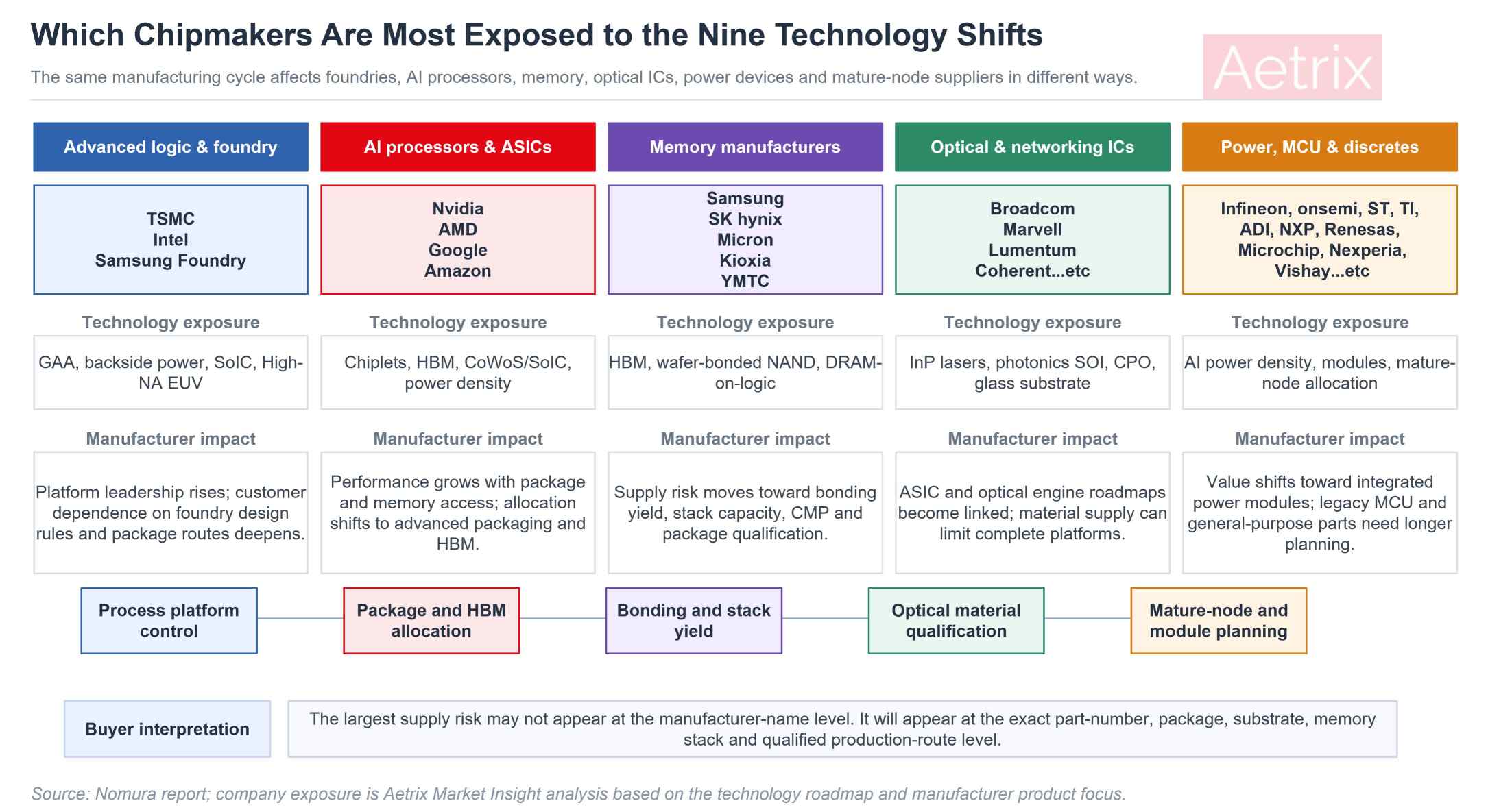
For chipmakers, the commercial impact is direct. TSMC, Intel and Samsung Foundry need to turn GAA, backside power delivery, High-NA EUV and advanced packaging into reliable platforms for Nvidia, AMD, Google, Amazon and other high-volume AI customers. Samsung, SK hynix, Micron, Kioxia and YMTC need to add more bonding and package capability to memory roadmaps. Broadcom, Marvell, Lumentum and Coherent sit near the center of the optical transition. Infineon, onsemi, STMicroelectronics, Texas Instruments, Analog Devices, NXP, Renesas, Microchip, Nexperia and Vishay face a different but related shift as AI power density and capital allocation reshape demand for power devices, MCU platforms and long-lifecycle components.
Nomura's report is primarily written from a semiconductor equipment and materials perspective. Aetrix reads the same technology cycle from a component supply perspective. The question for buyers is how these changes move into exact part numbers, package types, production routes, lead times, quote validity, MOQ, NCNR exposure and alternative-design decisions.
Key Findings
- Nomura identifies nine semiconductor technologies with expected 2025-2030 CAGR above 20%, 30% or 40%, including GAA, SoIC, glass core substrates, backside power delivery, bonded memory, InP lasers, photonics SOI and High-NA EUV.
- TSMC, Intel and Samsung Foundry gain more platform control as logic scaling moves into GAA, backside power, High-NA EUV, SoIC and package-level design.
- Nvidia, AMD, Google and Amazon benefit from advanced packaging and memory bandwidth, while their supply risk becomes more dependent on HBM, CoWoS/SoIC-class capacity, substrates and power delivery.
- Samsung, SK hynix, Micron, Kioxia and YMTC face a memory roadmap increasingly shaped by wafer bonding, stack yield, CMP, thinning and package-level qualification.
- Broadcom, Marvell, Lumentum and Coherent are exposed to the optical transition through InP lasers, photonics SOI, CPO and large networking packages.
- Infineon, onsemi, ST, TI and ADI can capture higher AI power-system content, with more value moving toward integrated power stages, modules, drivers, sensing and high-current packages.
- ST, NXP, Renesas and Microchip may face a more indirect effect through mature-node capacity decisions, product-family migration and long-range customer forecast requirements.
- Component buyers should review exact part numbers, package routes, bonding exposure, substrate availability and qualified alternates instead of relying only on manufacturer-level supply status.
What Nomura Means by a Semiconductor Renaissance
Nomura's semiconductor renaissance thesis does not imply that advanced-node migration stops. The report leaves room for continued pitch scaling if High-NA EUV becomes cost-effective at future nodes such as A10. The change is that scaling alone cannot satisfy every AI requirement across compute performance, power savings, heat dissipation, data bandwidth, optical transmission and physical-interface response.
This creates a broader manufacturing race. GAA improves transistor electrostatic control. Backside power delivery moves the power network away from the frontside signal network. SoIC and hybrid bonding allow vertically integrated dies. Wafer-bonded NAND and DRAM-on-logic improve memory density and bandwidth. InP lasers, photonics SOI and glass core substrates support faster AI networking and larger package footprints.
The business consequence is a deeper link between chip design and manufacturing infrastructure. A Nvidia accelerator, an AMD chiplet processor, a Google TPU, an Amazon Trainium device or a Broadcom switch ASIC increasingly depends on a complete platform: foundry node, package capacity, substrate choice, HBM availability, optical-engine roadmap, power-delivery architecture and qualified materials.
Nine Technologies Reshaping Chipmakers Through 2030
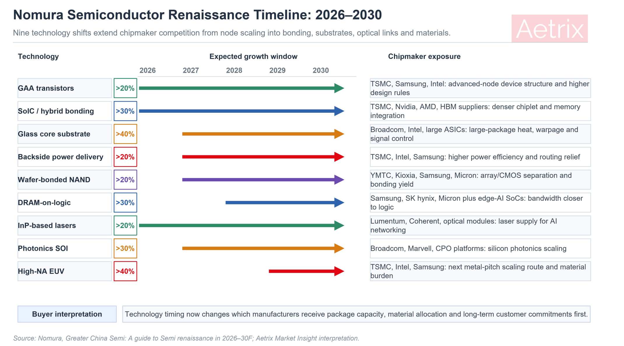
Nomura's technology table lists nine key areas, each with a different growth window and manufacturing requirement. Several begin growing from 2026, while glass core substrates, backside power delivery, wafer-bonded NAND and photonics SOI are more closely tied to the 2027 window. DRAM-on-logic begins later, and High-NA EUV is expected to grow from 2029 at the earliest if major customers adopt it.
| Technology | Nomura 2025-2030 CAGR | Expected Growth Start | Chipmaker Exposure |
|---|---|---|---|
| GAA transistors | >20% | 2026 | TSMC, Samsung and Intel compete through advanced transistor structures and tighter process integration. |
| SoIC and hybrid bonding | >30% | 2026 | TSMC, Nvidia, AMD and HBM suppliers depend on die-to-die bandwidth, bonding precision and package capacity. |
| Glass core substrates | >40% | 2027 at the earliest | Broadcom, Intel and large ASIC suppliers gain a possible path for bigger packages, lower warpage and high-speed signaling. |
| Backside power delivery | >20% | 2027 | TSMC, Intel and Samsung use backside power to reduce routing congestion and improve power delivery in advanced logic. |
| Wafer-bonded NAND | >20% | 2027 | YMTC, Kioxia, Samsung and Micron face more bonding, alignment, CMP and wafer-consumption exposure. |
| DRAM-on-logic | >30% | 2028 | Samsung, SK hynix, Micron and edge-AI chipmakers gain a route toward higher local memory bandwidth. |
| InP-based lasers | >20% | 2026 | Lumentum, Coherent and optical-module suppliers become more critical to AI-networking capacity. |
| Photonics SOI | >30% | 2027 | Broadcom, Marvell and CPO platforms use photonics SOI to scale compact optical engines. |
| High-NA EUV | >40% | 2029 at the earliest | TSMC, Intel and Samsung use the technology path to extend advanced-node scaling if cost and yield support adoption. |
Why the Value of a Chip Is Moving Into Materials, Packaging and Platform Control
Nomura estimates global semiconductor material sales at USD73.6 billion in 2025 and USD130.1 billion in 2030, a 12.1% CAGR. IC manufacturing materials are forecast to rise from USD46.5 billion to USD85.0 billion, while IC packaging materials are forecast to rise from USD27.1 billion to USD45.1 billion. The report also expects wafer, CMP, photoresist and packaging substrate to gain share inside the materials mix.
This matters commercially for manufacturers. A TSMC or Samsung customer is no longer buying only a process node. It is buying a manufacturing route that includes qualified wafers, photoresist, CMP slurries, bonding equipment, substrate supply and package assembly. A Nvidia GPU, AMD accelerator, Broadcom switch ASIC or Google TPU can face a delivery constraint at the package or HBM stage even after the logic die has been fabricated.
For component buyers, the supply signal moves downstream. The earliest sign of tightness may appear as longer lead times on selected orderable part numbers, package-specific allocation, stricter cancellation terms, or a manufacturer request for longer forecast visibility. This has already become visible in parts of the analog and MCU market. Aetrix previously covered Analog Devices' lead-time tightening and six-month order planning signal, and a similar logic applies when advanced manufacturing capacity reshapes internal allocation priorities.
How TSMC, Intel and Samsung Could Extend Advanced Logic Leadership
TSMC is the clearest example of the platform effect. Nomura connects TSMC to several layers of the transition: SoIC capacity expansion, future High-NA EUV decisions, local sourcing and a possible capital-spending surge. The report estimates TSMC could spend up to USD70 billion in capex in 2027 if more than ten fab modules expand simultaneously across Taiwan and overseas.
TSMC's advantage comes from the ability to offer advanced process nodes, CoWoS, SoIC and customer-specific qualification under one ecosystem. Nvidia, AMD, Broadcom, Google and Amazon can gain performance, but they also become more dependent on TSMC's packaging roadmap, material qualification and supplier allocation. A shortage in CoWoS-class capacity, HBM supply, substrates or high-end wafers can delay finished processors even when the design has strong demand.
Intel is exposed through a different route. PowerVia, Foveros, EMIB and glass-substrate research give Intel a chance to link front-end logic, backside power and advanced packaging more tightly. Nomura also discusses Intel's EMIB-T direction and notes that leading substrate companies may prioritize Intel-related capacity over early glass-core substrate ramps in some cases. If Intel can execute across logic nodes and packaging, it can offer AI and HPC customers an alternative advanced platform. If utilization or yield lags, the same technologies increase capital burden and execution risk.
Samsung Foundry faces a similar strategic test. GAA, backside power, advanced packaging and memory integration can strengthen Samsung's position when combined with its DRAM and HBM ecosystem. The challenge is credibility at the full platform level: logic yield, packaging capacity, memory qualification and customer commitment need to move together.
What Backside Power and SoIC Mean for Nvidia, AMD, Google and Amazon
AI chip companies are the largest immediate users of the semiconductor renaissance. Nvidia's GPUs, AMD's chiplet processors and accelerators, Google's TPU programs and Amazon's Trainium and Inferentia platforms all need more memory bandwidth, lower power loss and higher package density.
Backside power delivery can help advanced logic chips by reducing frontside routing congestion and improving power delivery. For companies designing very large AI dies or multi-die processors, that can support higher performance per watt. The cost is tighter co-design with the foundry. Physical design, power-grid layout, thermal behavior and package routing become more specific to each manufacturing platform.
SoIC and hybrid bonding also change sourcing behavior. A chiplet architecture gives AMD and other processor designers flexibility to mix nodes and functions. It can also create a new bottleneck when package capacity or bonding yield is limited. Nvidia's strong AI demand, Google's TPU roadmap and Amazon's custom silicon programs increase competition for the same advanced-packaging and HBM resources.
The buyer-side effect is longer planning. A customer buying boards, servers or modules built around these processors needs to monitor the whole ecosystem: processor allocation, HBM availability, package capacity, power module supply, cooling hardware and optical-networking components. A CPU or GPU part number may be listed as active while the platform remains constrained by another critical element.
How Samsung, SK hynix, Micron, Kioxia and YMTC Face the Bonded-Memory Shift
Memory manufacturers are entering a phase where bonding and packaging matter as much as cell density for premium products. HBM already shows this pattern. Samsung, SK hynix and Micron can compete on DRAM technology, but final supply depends on stacking, packaging, thermal behavior, GPU qualification and customer-specific validation.
Nomura also highlights wafer-bonded NAND and DRAM-on-logic. Wafer-bonded NAND separates the CMOS logic and memory-cell array into different wafer flows before bonding. YMTC's Xtacking technology is a major example of this architecture, while Kioxia has also been used in Nomura's report to explain CMOS-bonded array structures.
For YMTC, bonded NAND shows how structural innovation can narrow part of the gap with larger global memory suppliers. For Kioxia, Samsung and Micron, it raises the need to protect NAND competitiveness through bonding, CMP, alignment and parallel wafer processing. The supply-chain burden rises because one finished memory product may depend on two wafer flows and a high-yield bonding step.
DRAM-on-logic adds another layer. Nomura expects stronger momentum from 2028, led by edge AI, automotive smart cockpits, premium PCs and robotics. Samsung, SK hynix and Micron will need to decide how far they participate directly and how much they rely on foundry or packaging partners. The product may look like memory to the end customer, while its supply risk looks closer to a heterogeneous integration platform.
Why Broadcom, Marvell, Lumentum and Coherent Sit at the Center of Optical Integration
AI networking pushes the bottleneck from computation into data movement. Nomura expects the optical transceiver cycle to continue into 2027, driven by 1.6T upgrades, silicon photonics migration and the development of LPO, LRO, NPO and CPO architectures. InP remains critical for EML and CW lasers, while photonics SOI supports scalable photonic integrated circuits.
Broadcom and Marvell are exposed at the network ASIC, DSP and silicon-photonics platform level. A switch ASIC vendor that can align silicon, optical engines and package integration can capture more system value. Broadcom is also highlighted by Nomura as a likely early mover in glass core substrate adoption, potentially for switch ASICs from 2027 at the earliest.
Lumentum and Coherent sit closer to the optical component layer. Their exposure comes from InP lasers and high-speed optical device demand. A shortage in InP substrates, laser dies, photonics SOI wafers or fiber-attach packaging can restrict the complete optical platform, even if the network ASIC itself is available.
For buyers, the practical lesson is that optical supply should be checked as a full engine. DSP, laser, modulator, photodetector, photonics substrate and package qualification all matter. A replacement optical module or CPO platform may require extensive system validation rather than a simple supplier swap.
What Glass Core Substrates Could Mean for Broadcom, Intel and Large ASIC Packages
Glass core substrates are one of the clearest examples of the opportunity and risk in the next cycle. Large AI and networking chips stress organic substrates through warpage, thermal expansion, via pitch and dielectric loss. Glass offers better flatness, lower warpage, better heat spreading and high-speed signaling advantages.
Nomura says Broadcom is likely to be an early mover in glass core substrates, possibly first on a switch ASIC from 2027 at the earliest. Intel has publicly demonstrated glass core substrates for next-generation advanced packaging, framing the work as foundational for the latter part of the decade. These roadmaps point to large ASICs and advanced packages as the first meaningful use cases.
The cost and manufacturing risk remain high. Nomura notes that current TGV processing with small trial volumes can cost USD400-500 per unit, while total glass core substrate ASP could exceed USD1,500, far above a large ABF substrate. The report also identifies RDL dielectric peeling and delamination as a technical bottleneck, with coefficient-of-thermal-expansion mismatch and adhesion between glass, ABF and copper remaining fundamental challenges.
For buyers, early glass-core packages should be treated as platform-specific. A product using glass may not have a fast alternative in ABF without package, board and reliability requalification. During early adoption, substrate allocation can become as important as silicon availability.
What the AI Power Shift Means for Infineon, onsemi, ST, TI and ADI
Backside power delivery is an internal logic-wafer architecture, so it should not be confused with ordinary MOSFET, IGBT or power module design. The effect on power semiconductor manufacturers comes through system-level power density. AI accelerators require higher current, lower voltage, faster transient response and tighter thermal design.
Infineon and onsemi can benefit from server power, high-efficiency conversion, SiC, GaN, MOSFETs and integrated power modules. The opportunity is strongest where customers need validated power stages, high-current packages, thermal reliability and system-level support. Commodity discrete transistors may see less benefit if customers move toward integrated modules or package-level power delivery.
STMicroelectronics participates through power devices, smart power products, industrial ICs and MCU platforms. Its opportunity is tied to automotive, industrial automation, motor control, energy infrastructure and higher-value embedded systems. The same company also manages a long tail of mature MCU and legacy products, so allocation decisions can differ significantly by family, process node and package.
Texas Instruments and Analog Devices are positioned differently. Their exposure is less about discrete transistors and more about PMICs, multiphase controllers, current sensing, isolation, clocking, data conversion and signal-chain content inside AI and industrial systems. Higher system complexity can raise the value of high-performance analog content, while long-tail industrial products may require longer forecasting when manufacturing resources are pulled toward data-center and automotive programs.
For buyers, power-device sourcing should move from part-level comparison to system-level evaluation. A lower-priced MOSFET may lose to a more integrated power stage if the module reduces thermal risk, board area or validation effort. At the same time, high-volume legacy discrete products should be monitored for die, package and assembly allocation if suppliers prioritize higher-margin modules.
How Capital Reallocation Could Affect ST, NXP, Renesas, Microchip, Nexperia and Vishay Buyers
Mature-node and long-lifecycle manufacturers are not outside the semiconductor renaissance. They may be less directly exposed to High-NA EUV or GAA, yet they still compete for capital, packaging resources, engineering attention and customer forecasts within the same global supply chain.
STMicroelectronics, NXP, Renesas and Microchip operate broad MCU, automotive, industrial and mixed-signal portfolios. These companies will continue supporting mature products, but new investment tends to favor automotive, security, connectivity, edge AI and higher-value industrial platforms. Older product families, small-volume packages and lower-margin orderable parts may receive less capacity expansion even when demand remains steady.
Nexperia and Vishay represent another side of the issue. Discrete transistors, diodes and protection devices are usually more mature, but they still rely on wafer starts, assembly capacity, lead frames, copper, testing and logistics. If higher-value power modules, automotive products or data-center devices receive priority, some standard components can experience longer lead times without a headline industry shortage.
For OEMs and EMS providers, this creates two separate tasks. New designs should consider whether the manufacturer is actively investing in the chosen platform. Existing designs should identify single-source legacy parts, rare packages, special temperature grades and devices with low substitution flexibility. The risk is often hidden in the suffix of the exact part number rather than the product family name.
Manufacturer Impact Table
| Manufacturer | Technology Exposure | Potential Advantage | Supply-Chain Risk | Buyer Impact |
|---|---|---|---|---|
| TSMC | GAA, SoIC, backside power, High-NA EUV, CoWoS | Stronger platform control across process and package | Capex, yield and advanced packaging allocation | More dependence on package route and customer priority |
| Intel | PowerVia, Foveros, EMIB, EMIB-T, glass substrates | Alternative advanced logic and packaging platform | Execution, utilization and customer adoption | Potential second source for advanced packaging, with qualification work |
| Nvidia | HBM, CoWoS-class packaging, high-density power, optical links | AI ecosystem control | Packaging, HBM and power infrastructure allocation | Long planning horizons for GPU systems and modules |
| AMD | Chiplets, 3D V-Cache, advanced packaging | Flexible node mixing and package-level scaling | Foundry and packaging dependence | Package-specific availability and validation requirements |
| Broadcom | Switch ASICs, CPO, silicon photonics, glass substrates | Networking platform integration | TGV, substrate cost and optical-engine qualification | Early products may have limited package alternatives |
| Samsung, SK hynix, Micron | HBM, DRAM-on-logic, advanced memory packaging | Premium memory content and AI platform qualification | Bonding, stack yield and customer allocation | Tight allocation by density, stack, package and customer program |
| Kioxia, YMTC | Wafer-bonded NAND, CBA/Xtacking-type architectures | Higher NAND density and separated logic/array optimization | Two-wafer flow, bonding yield and CMP consumption | Availability may differ sharply by product generation and package |
| Infineon, onsemi | Power modules, MOSFETs, SiC, GaN, high-current packages | AI server and energy-infrastructure power demand | Thermal package qualification and module capacity | Integrated alternatives may replace some discrete designs |
| ST, NXP, Renesas, Microchip | MCU, automotive, industrial, mixed-signal and long-life products | Higher-value embedded platforms and industrial/automotive demand | Mature-node investment and legacy-product allocation | Earlier migration planning for older part families |
| TI, ADI | PMICs, multiphase controllers, signal chain, current sensing, isolation | Higher analog and power-management content in AI and industrial systems | Portfolio prioritization and long-tail product availability | More demand visibility may be required for selected devices |
Supply-Chain Implications for Component Buyers
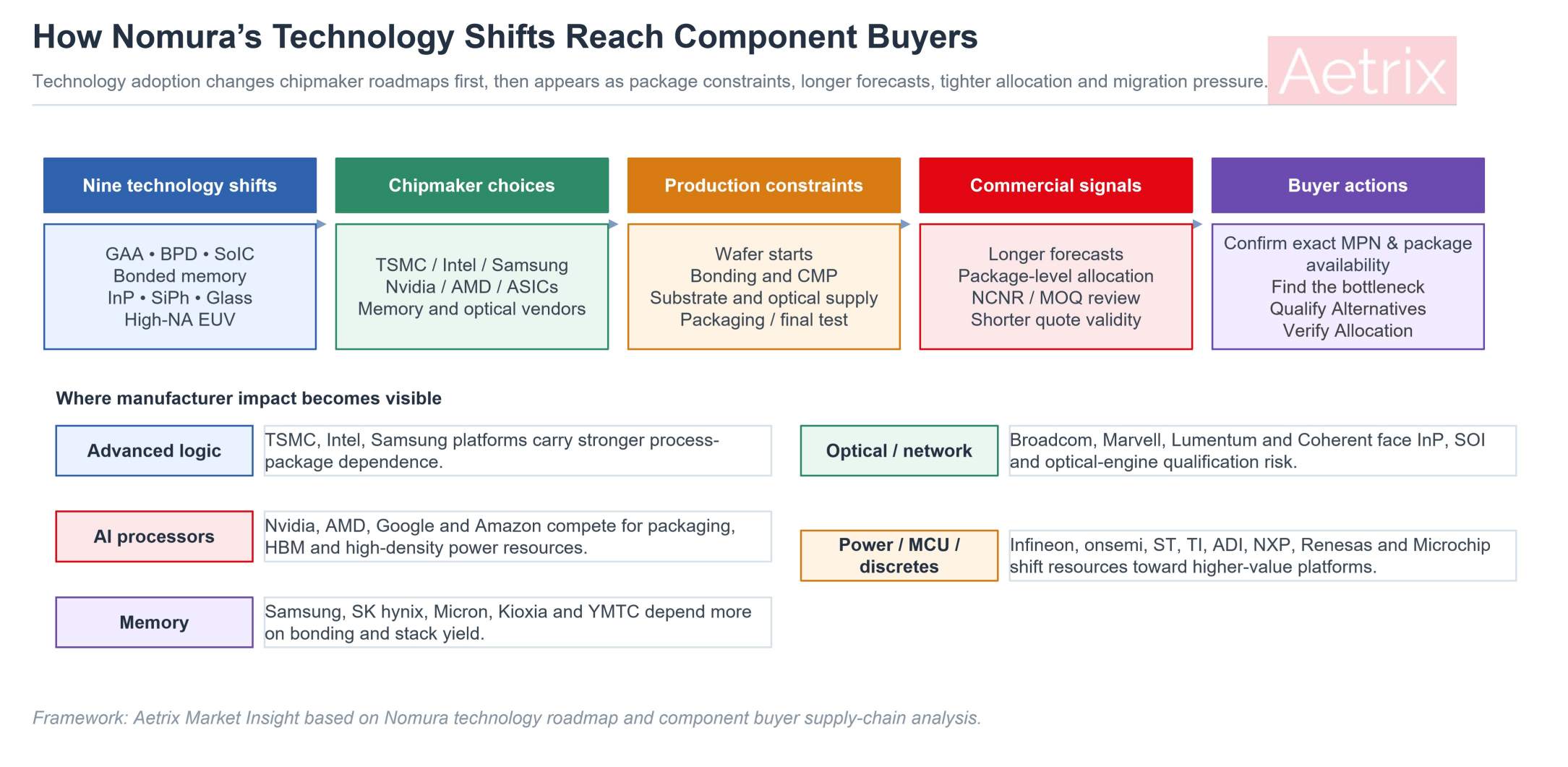
The main procurement change is that availability must be evaluated by route, not just by manufacturer. A part supplied by a strong manufacturer can still be constrained if it uses a tight package, a limited substrate, a new bonding process, or a customer-specific optical platform.
For advanced processors, buyers should track HBM allocation, substrate capacity, package qualification and power-module supply. For memory, buyers should track exact density, stack, interface, package and qualification status. For optical products, buyers should confirm whether the constraint sits in the DSP, laser, photonics SOI, InP substrate, FAU, fiber attach or final module assembly.
For power devices, the comparison should include system cost. Infineon or onsemi modules may cost more than discrete MOSFET combinations, but they can reduce thermal and validation risk. For MCU and general-purpose analog devices, buyers should check whether the product family remains a priority platform for the manufacturer or is being supported mainly for installed-base demand.
What Buyers Should Monitor from 2026 to 2030
The first signal is foundry platform adoption. If TSMC, Intel and Samsung move GAA, backside power and SoIC into more customer programs, early allocation will favor large customers that can commit volume and share long-term demand visibility.
The second signal is packaging capacity. CoWoS, SoIC, EMIB, Foveros, HBM stacks, wafer bonding and glass core substrates each create their own supply cycle. Buyers should not assume that available wafer starts automatically translate into available finished components.
The third signal is optical-material supply. InP lasers and photonics SOI will increasingly influence the delivery of AI networking platforms. Broadcom and Marvell switch platforms, Lumentum and Coherent optical components, and CPO-related modules should be evaluated as complete optical supply chains.
The fourth signal is mature-product prioritization. ST, NXP, Renesas, Microchip, TI and ADI can continue shipping long-life products while still asking for longer forecasts on selected part numbers. When manufacturers move capital toward automotive, AI, data-center power or advanced packaging, buyers of older packages and low-margin devices may need earlier backlog coverage.
Key Takeaways
- Nomura's semiconductor renaissance is a chipmaker roadmap issue, not only a materials and equipment issue.
- TSMC, Intel and Samsung gain more leverage when process, package, substrate and material qualification become one platform.
- Nvidia, AMD, Google and Amazon will compete for advanced packaging, HBM, substrates and power-delivery resources alongside logic wafer capacity.
- Samsung, SK hynix, Micron, Kioxia and YMTC need to manage bonded-memory yield, CMP, wafer consumption and package qualification.
- Broadcom, Marvell, Lumentum and Coherent are positioned around InP, photonics SOI, CPO and optical-engine integration.
- Infineon, onsemi, ST, TI and ADI can benefit from higher power density, but value may shift from commodity discretes toward integrated modules and validated power stages.
- ST, NXP, Renesas and Microchip buyers should watch platform migration, mature-node allocation and long-lifecycle product support.
- Availability will increasingly be determined at the exact MPN and package level, with substrate, memory configuration and qualified production route shaping lead times more than broad product-family availability.
- Buyers should qualify alternate platforms early, especially for devices tied to new packages, bonded memory, optical engines or long-life mature-node products.
The next semiconductor cycle will reward manufacturers that control more than transistor scaling. The leading companies will be those able to align process nodes, power delivery, bonding, substrates, memory bandwidth and optical connectivity into manufacturable platforms. For buyers, the supply chain will become more technical and more part-number-specific. Factory lead time, spot-market availability and long-term product support will increasingly depend on the manufacturing route behind the device, not only on the brand printed on the package.