
 My Inquiry
 My Account


Schmitt Trigger Explained: Hysteresis, Circuits, Inverters and Applications
Article Details
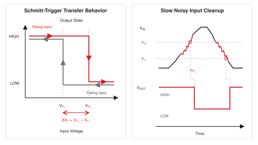
A Schmitt trigger converts a slow, noisy or irregular voltage transition into a clean digital state by using two switching thresholds instead of one. A rising input must cross the positive-going threshold, VT+, before the output changes. The output will not change back until the input falls through the lower negative-going threshold, VT−. The separation between those thresholds is hysteresis.
That directional behavior is the practical difference between a Schmitt-trigger input and an ordinary logic input. It prevents small voltage excursions near one threshold from repeatedly toggling the following logic. It does not remove noise from the wire, protect an overvoltage input or make incompatible logic levels compatible.
Rising input transition: switch at VT+
Falling input transition: switch at VT−
Hysteresis width: ΔVT = VT+ − VT−
Between VT− and VT+, the output retains the state established by the previous crossing.
What a Schmitt Trigger Changes
An ordinary digital receiver guarantees LOW below VIL(max) and HIGH above VIH(min). The region between them is not a permitted steady-state logic level, but that alone does not prove that the input has hysteresis. A true Schmitt-trigger input has direction-dependent switching thresholds and normally specifies VT+, VT− and either a minimum hysteresis value or enough limits to determine it.
| Input Type | Switching Behavior | Best Use | Design Limitation |
|---|---|---|---|
| Ordinary logic input | Recognizes guaranteed LOW and HIGH ranges; no separate rising and falling threshold is implied. | Clean, fast digital signals that meet input transition requirements. | A slow or noisy crossing can produce extra transitions or excessive supply current. |
| Integrated Schmitt input | Uses VT+ on a rising input and VT− on a falling input. | Switches, RC nodes, sensors, long control lines and slow power-related signals. | Thresholds vary with supply, temperature and device family; input ratings still apply. |
| Comparator with positive feedback | External feedback creates two thresholds around a chosen reference. | Adjustable trip points, asymmetric thresholds and analog sensor conditioning. | Requires calculations for output swing, reference accuracy, bias current and source impedance. |
How Hysteresis Rejects Threshold Noise
Consider a non-inverting Schmitt input that has already switched HIGH. The next permitted transition is not another crossing of VT+; the input must fall below VT−. Noise that moves the input around the upper threshold but never reaches the lower threshold therefore cannot switch the output LOW. An inverting Schmitt trigger uses the same thresholds but reverses the output polarity.
The hysteresis width is not a universal "maximum noise amplitude." Noise immunity depends on the current output state, the DC input level, the direction of travel and the worst-case threshold limits. A disturbance can be smaller than ΔVT and still cause a transition if the undisturbed input is already close enough to the threshold that must be crossed.
Reading VT+, VT− and ΔVT Correctly
- VT+(max) is the conservative threshold for proving that a rising input will switch every compliant device under the stated conditions.
- VT−(min) is the conservative threshold for proving that a falling input will switch every compliant device.
- ΔVT(min) is the smallest guaranteed separation between the two thresholds on an individual device.
- Typical threshold curves describe representative behavior. They are useful for estimating but not for a worst-case interface decision.
- The threshold table is valid only for its stated VCC, temperature and test conditions.
Minimum and maximum threshold ranges can overlap when values from different production units are placed on one chart. That does not mean an individual Schmitt input has reversed hysteresis. Use the guaranteed hysteresis specification and the threshold limits according to the manufacturer's definitions.
A Simple Threshold Example
For an idealized device with VT+ = 2.0 V and VT− = 1.2 V:
On a rising input, 1.8 V is not enough to command the transition; the input must reach 2.0 V. After the output changes, an input that moves between 1.3 V and 1.7 V remains inside the hysteresis band and preserves the new state. The output changes back only after the input falls below 1.2 V. These values illustrate the behavior and are not specifications for a logic family.
Inverting and Non-Inverting Schmitt Triggers
Hysteresis and polarity are separate properties. The familiar 74HC14 and 74HCT14 are inverting devices. Parts such as the SN74LVC1G17 provide a non-inverting Schmitt-trigger buffer. The symbol's output bubble identifies inversion; the hysteresis symbol at the input identifies Schmitt behavior.
| Input Event | Inverting Schmitt Trigger | Non-Inverting Schmitt Trigger |
|---|---|---|
| Input rises through VT+ | Output changes from HIGH to LOW. | Output changes from LOW to HIGH. |
| Input remains between thresholds | Output holds its previous state. | Output holds its previous state. |
| Input falls through VT− | Output changes from LOW to HIGH. | Output changes from HIGH to LOW. |
The output memory inside the hysteresis band does not make a Schmitt gate a general-purpose latch. There is one signal input, and the stored state is only the consequence of the two switching thresholds. For set/reset and data-storage behavior, see the SR and D latch circuit guide.
Choosing a Schmitt-Trigger Logic Family
The number "14" commonly identifies an inverting Schmitt-trigger function and "17" a non-inverting buffer function, but the family prefix controls supply range, thresholds, speed, drive, input protection and power-off behavior. A matching pinout is not enough to approve a substitution.
| Example Device | Configuration | Published Supply Range | Useful Selection Point | Check Before Use |
|---|---|---|---|---|
| 74HC14 | Six inverting Schmitt gates | 2.0 V to 6.0 V for the cited Nexperia device | CMOS-family operation over several common logic rails. | VT+ can be too high for a weak 3.3 V source when the gate is powered near 5 V. |
| 74HCT14 | Six inverting Schmitt gates | 4.5 V to 5.5 V for the cited Nexperia device | Lower, TTL-compatible input thresholds at a 5 V-class supply. | It is not a 3.3 V-powered part, and its 5 V CMOS output can overstress a non-tolerant 3.3 V receiver. |
| CD40106B | Six inverting Schmitt gates | 3 V to 18 V for the cited TI device | Wide-supply control, wave shaping and low-frequency RC timing. | Delay and output drive differ greatly from newer 74-series families. |
| SN74LVC1G14 | One inverting Schmitt gate | 1.65 V to 5.5 V | Small single-gate implementation; TI specifies partial-power-down Ioff. | Use the exact package pinout and verify input-voltage limits at the selected VCC. |
| SN74LVC1G17 | One non-inverting Schmitt buffer | 1.65 V to 5.5 V | Preserves polarity while cleaning a slow or noisy input. | Confirm output current, load capacitance and power sequencing. |
Supply ranges above belong to the linked manufacturer data, not to every part carrying a similar base number. Automotive qualification, extended temperature grade, package suffix and input overvoltage tolerance are orderable-part attributes.
74HC14 Versus 74HCT14 at a 4.5 V Supply
The Nexperia 74HC14/74HCT14 data sheet shows why "HC" and "HCT" cannot be treated as interchangeable input standards. Over −40 °C to +125 °C at VCC = 4.5 V, the cited 74HC14 specifies VT+ from 1.7 V to 3.15 V, VT− from 0.9 V to 2.0 V and hysteresis from 0.4 V to 1.4 V. The cited 74HCT14 specifies VT+ from 1.2 V to 1.9 V, VT− from 0.5 V to 1.2 V and at least 0.4 V of hysteresis.
Take an illustrative 3.3 V driver that guarantees VOH(min) = 2.4 V and VOL(max) = 0.4 V under the intended load:
| Receiver | Rising-State Margin | Falling-State Margin | DC Threshold Result |
|---|---|---|---|
| Nexperia 74HC14 at 4.5 V | 2.4 V − 3.15 V = −0.75 V | 0.9 V − 0.4 V = +0.5 V | Not guaranteed because the rising-state margin is negative. |
| Nexperia 74HCT14 at 4.5 V | 2.4 V − 1.9 V = +0.5 V | 0.5 V − 0.4 V = +0.1 V | Both threshold checks pass under the stated conditions. |
The example does not claim that every 3.3 V output has those guarantees or that every 5 V HC input fails. Read the actual output limits at the real load and the receiver thresholds at the real supply. The TTL versus CMOS logic-level guide covers the family-level interface checks in more detail.
Designing a Comparator Schmitt Trigger
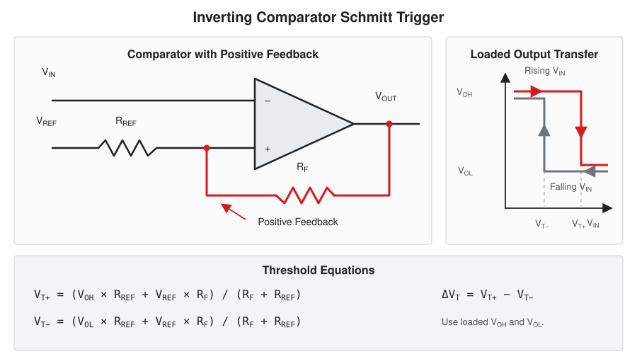
A comparator becomes a Schmitt trigger when a controlled amount of its output is returned to the non-inverting input as positive feedback. Unlike a fixed-threshold logic gate, this circuit can place the switching window around a chosen reference and set its width with resistor ratios.
For an inverting comparator circuit, apply VIN to the inverting input. Connect RF from the output to the non-inverting threshold node and RREF from that node to VREF. Assuming comparator input current is negligible, the two thresholds are:
These expressions use the loaded output levels, not ideal supply rails. An open-drain comparator's VOH is established by the pull-up supply, pull-up resistance, load and leakage. VOL depends on sink current. A push-pull comparator has different output-swing limits.
Worked Threshold Calculation
Suppose VREF = 2.5 V, VOH = 4.8 V, VOL = 0.1 V, RF = 100 kΩ and RREF = 20 kΩ:
A rising VIN switches the inverting comparator output LOW at approximately 2.883 V. The lower output shifts the threshold to 2.100 V; VIN must then fall below that value before the output returns HIGH. Resistor tolerance, reference error, input offset voltage, input bias current and loaded output swing all move the real limits.
Comparator or Op Amp?
A comparator is normally the safer choice for threshold detection because it is designed for open-loop switching and specifies propagation delay, input overdrive behavior and output logic conditions. An op amp may work in a low-speed Schmitt trigger only when its data sheet permits the expected differential input voltage, common-mode range, output saturation and recovery behavior.
Some op amps recover slowly after the output saturates; some have input structures that behave unexpectedly when a pin approaches or exceeds a rail. Do not approve an op amp Schmitt circuit from a simulation built with an ideal amplifier. The op amp fundamentals and feedback guide provides the underlying input, output and stability checks.
Schmitt Trigger RC Oscillator
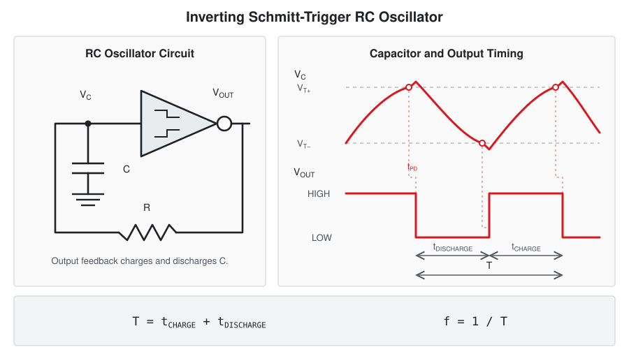
An inverting Schmitt gate can form a relaxation oscillator with one resistor from output to input and one capacitor from input to ground. When the output is HIGH, the capacitor charges through R until the input reaches VT+. The gate then drives LOW. The capacitor discharges until it reaches VT−, and the cycle repeats.
Using the actual output levels and thresholds, the ideal charge and discharge intervals are:
If an ideal gate switches at 0.7VCC and 0.3VCC with rail-to-rail output, each half-cycle is approximately 0.847RC and the frequency is approximately 0.590/RC. With R = 100 kΩ and C = 10 nF, RC = 1 ms and the ideal estimate is about 590 Hz.
The Aetrix RC time constant calculator can check τ = RC. Use the equations above for oscillator period because the capacitor does not charge from 0% to 100%; it moves only between the device's two thresholds.
RC Oscillator Layout and Component Checks
- Place the timing resistor and capacitor close to the gate input so the high-impedance node does not collect switching noise.
- Keep the output trace away from the timing node except for the intentional feedback resistor connection.
- Use a resistor low enough that input leakage and PCB contamination current are negligible relative to RC current.
- Use a stable capacitor dielectric when frequency drift matters; high-value Class 2 ceramics can vary with bias, temperature and age.
- Add local supply decoupling, commonly 100 nF close to the package, and verify the manufacturer's recommendations.
- Tie every unused CMOS input to a defined HIGH or LOW level. Do not leave spare Schmitt inputs floating.
Where Schmitt Trigger Circuits Work Well
| Application | What the Hysteresis Solves | What Still Needs Engineering |
|---|---|---|
| Mechanical switch input | Converts an RC-filtered transition into one clean logic edge. | Choose RC so contact bounce does not cross both thresholds; long bounce may still need firmware or a dedicated debouncer. |
| Slow sensor or open-collector signal | Prevents repeated toggling while the voltage moves slowly through the threshold region. | Check pull-up resistance, sensor leakage, edge time, input clamp current and logic-level compatibility. |
| Long cable or harness control | Adds immunity to threshold-region ringing and coupled noise. | Add the required surge, ESD, filtering, grounding and cable termination. A Schmitt input is not line protection. |
| Sine or triangle wave shaping | Produces a digital edge at repeatable direction-dependent thresholds. | Input amplitude must cross both guaranteed thresholds; frequency is limited by propagation delay and output loading. |
| RC power-on signal | Turns a slow capacitor ramp into a distinct digital transition. | Verify power ramp, capacitor discharge between cycles, minimum pulse width and powered-off pin current. Use a supervisor for critical reset timing. |
| Simple relaxation oscillator | Provides the two trip points needed for repetitive capacitor charge and discharge. | Accept threshold and component tolerance; control leakage and PCB parasitics. |
| Clock or interrupt cleanup | Removes extra transitions caused by a slow or moderately noisy edge. | Account for added delay, threshold-induced timing variation and duty-cycle distortion; use a specified clock receiver for low-jitter paths. |
What a Schmitt Trigger Does Not Fix
- Overvoltage: a 5 V signal can still damage or back-power a 3.3 V Schmitt input that is not explicitly tolerant.
- Insufficient amplitude: a waveform that never exceeds VT+(max) or never falls below VT−(min) is not guaranteed to switch.
- Wide glitches: any disturbance that crosses the active threshold for long enough can propagate to the output.
- Ground offset: thresholds are referenced to the receiver ground. Cable current and ground potential difference change the voltage seen at the pin.
- Analog accuracy: logic Schmitt thresholds often have wide production spread and are unsuitable as precision measurement references.
- Uncontrolled startup: the output may not be valid below the minimum operating supply, and an RC node may retain charge after a short power interruption.
- Metastability at a synchronous boundary: a clean asynchronous edge still needs synchronization before entering synchronous state logic.
A Worst-Case Design Procedure
- Define the signal at the receiver pin. Record minimum HIGH, maximum LOW, source impedance, ramp rate, noise, ringing, cable length and off-state behavior.
- Check pin-voltage ratings first. Use recommended operating limits for normal behavior and absolute maximum ratings only as stress boundaries. Include every power sequence.
- Prove both transitions. Require VIN,HIGH(min) ≥ VT+(max) and VIN,LOW(max) ≤ VT−(min) at the actual supply and temperature.
- Check hysteresis against the disturbance. Model the direction and DC level of the signal rather than comparing a single noise number with typical ΔVT.
- Check timing. Include propagation delay, threshold variation, input slew, output load, pulse width and any synchronizer setup/hold requirement.
- Check current and power. A slow input may still increase CMOS supply current while the input voltage is away from a rail. Calculate output load and switching power.
- Check startup and shutdown. Define unused inputs, unpowered inputs, output state, capacitor discharge and reset behavior.
- Verify on hardware. Probe at the receiving pin with a short ground connection and test supply, temperature, noise and load corners that matter to the application.
Troubleshooting a Schmitt Trigger Circuit
| Symptom | Likely Cause | Useful Measurement | Corrective Action |
|---|---|---|---|
| Output toggles more than once | Input crosses both thresholds during ringing or switch bounce; supply noise moves the effective threshold. | Capture input and VCC at the IC pins with sufficient bandwidth. | Improve filtering, grounding, termination or hysteresis; shorten probe ground and decouple locally. |
| Output never changes HIGH or LOW | Input amplitude does not cross the required worst-case threshold, or polarity was misunderstood. | Measure input extrema and compare with VT+(max) and VT−(min). | Change threshold family, increase signal swing or use a comparator/translator. |
| HC gate works on one board but not another | Typical 3.3 V output reaches a 5 V HC threshold on some units but lacks guaranteed margin. | Compare driver VOH(min) under load with receiver VT+(max). | Use HCT/AHCT where valid or a specified level translator. |
| RC oscillator frequency is wrong | Actual thresholds, output swing, capacitor value or leakage differ from assumptions. | Measure VT+, VT−, capacitor ramp and output rails. | Recalculate with worst-case values or use a timing device with a frequency specification. |
| Supply current is unexpectedly high | Input spends substantial time between rails, an input floats, outputs contend or pin voltage exceeds a rail. | Check every input level, ΔICC conditions and output current. | Drive unused inputs, remove contention, shorten transition time or select a suitable input architecture. |
| Device is powered through its input | Driver remains active while the Schmitt gate supply is off and current flows through input protection. | Measure the unpowered VCC rail and input current during sequencing. | Use Ioff/partial-power-down-rated logic, isolate the signal or change sequencing. |
| Comparator chatters despite feedback | Hysteresis is too small, positive feedback is delayed by capacitance, or the reference/output is noisy. | Probe input, threshold node, reference and output at the comparator pins. | Increase calculated hysteresis, reduce node impedance, improve layout or choose a faster comparator. |
Schmitt Trigger Selection Checklist
- Required polarity and number of channels
- Recommended VCC range and temperature grade
- Guaranteed VT+, VT− and ΔVT limits
- Input voltage range, clamp behavior and partial-power-down rating
- Propagation delay, pulse-width response and channel skew
- Output VOH/VOL at the intended current and capacitance
- Supply current with slow or mid-rail inputs
- Package, pinout, assembly process and qualification status
- Defined state for every unused input
- Bench evidence at the receiving pin under relevant corner conditions
A Schmitt trigger should be selected from its guaranteed transfer limits, not from the gate symbol alone. The safest design establishes two facts independently: the input crosses both required thresholds during normal operation, and the pin remains inside its voltage and current ratings during every powered and unpowered condition.
Technical References
- Texas Instruments: Understanding Schmitt Triggers, SCEA046
- Nexperia: 74HC14; 74HCT14 Hex Inverting Schmitt Trigger Data Sheet
- Texas Instruments: CD40106B CMOS Hex Schmitt-Trigger Inverters Data Sheet
- Texas Instruments: SN74LVC1G14 Single Schmitt-Trigger Inverter
- Analog Devices: MT-083 Comparators
Frequently Asked Questions
What is a Schmitt trigger?
A Schmitt trigger is a threshold circuit with hysteresis. It uses a higher switching threshold for a rising input and a lower threshold for a falling input, allowing slow or noisy voltages to produce clean digital transitions.
Why does a Schmitt trigger have two thresholds?
The two thresholds prevent a small reversal or noise excursion near one switching point from immediately changing the output back. After one threshold is crossed, the opposite threshold must be crossed before another output transition occurs.
What is the difference between a Schmitt trigger and a comparator?
A comparator detects which of two input voltages is larger. A comparator becomes a Schmitt trigger when internal or external positive feedback creates separate rising and falling thresholds. Logic Schmitt gates contain fixed internal hysteresis; comparator circuits can provide adjustable thresholds.
What is the difference between 74HC14 and 74HCT14?
Both are hex inverting Schmitt-trigger devices, but the HCT version uses lower, TTL-compatible input thresholds and normally operates from a 5 V-class supply. HC uses CMOS-family thresholds and supports a wider supply range. Exact limits depend on the manufacturer and orderable device.
Can a Schmitt trigger convert 3.3 V logic to 5 V logic?
Only if the chosen input thresholds accept the 3.3 V driver's guaranteed output levels and all input-voltage ratings pass. A 5 V-powered HCT Schmitt gate can suit some fixed-direction interfaces, but it is not a universal or bidirectional level translator.
Can a Schmitt trigger debounce a mechanical switch?
It can clean the transition from a properly designed RC debounce network. Hysteresis alone does not guarantee removal of long or repeated contact bounce that crosses both thresholds.
Can an op amp be used as a Schmitt trigger?
Sometimes, but the op amp must tolerate open-loop operation, the input common-mode and differential voltages, output saturation and recovery. A comparator is usually better specified for threshold switching.
How accurate is a 74HC14 RC oscillator?
It is suitable for noncritical timing, but frequency can vary with threshold spread, supply voltage, temperature, resistor tolerance, capacitor tolerance, leakage and output swing. It should not replace a specified clock source where accuracy or jitter matters.
Does a Schmitt input allow any input rise or fall time?
Some true Schmitt devices explicitly allow unlimited input rise and fall time, while other parts provide only Schmitt-trigger action and retain transition-rate limits. The exact device data sheet decides.
What should be done with unused Schmitt-trigger inputs?
Tie every unused CMOS input to a defined permitted HIGH or LOW level. A floating input can switch unpredictably, increase supply current and couple noise into adjacent channels.


