My Inquiry
 My Account


Renesas Electronics announced on July 31, 2026 that production at its Takasaki Factory in Gunma Prefecture will be phased out over the next two to three years. The manufacturing site operates a 6-inch, or 150mm, wafer line. Factory closure will follow after production ends.
Renesas plans to assess customer demand and build the inventory required to support supply during the transition. The company will retain and strengthen the Takasaki-area research and development functions covering analog ICs and discrete power semiconductors, with future work focused on automotive and data center applications. (Renesas, Takasaki Factory Production Phase-Out Announcement)
The announcement begins a managed product-lifecycle transition. Factory output will continue while Renesas reviews demand, evaluates production transfers and prepares inventory. Supply exposure is expected to emerge gradually through manufacturing-site changes, product change notifications, last-time-buy programs and product-specific discontinuation decisions.
The central question for customers is which devices still depend on Takasaki-specific processes. Public records connect the factory with selected power MOSFET and switching products, analog ICs, IGBTs and power-diode dies. Renesas has yet to publish a complete list of affected orderable part numbers, making MPN-level wafer-source verification the starting point for procurement risk assessment.
Why the 6-Inch Line Is Reaching End of Life
Renesas attributes the phase-out to structural changes in the supply chain supporting 6-inch semiconductor production. Some production materials are being discontinued, maintenance support for older manufacturing equipment is becoming less available, and the factory's equipment and utility facilities are aging.
These problems can reach a critical point while the semiconductor products themselves remain commercially useful. Analog and power devices often stay in automotive, industrial, appliance and infrastructure designs for many years. Their production equipment, spare parts and supporting materials may have a shorter practical life.
A mature wafer line depends on a broad manufacturing ecosystem. Photolithography, diffusion, deposition, etching and ion-implantation tools require compatible replacement components, control electronics and technical support. The factory also needs stable supplies of wafers, gases, chemicals, metals and specialized consumables.
As worldwide 150mm production declines, equipment suppliers and material vendors have less incentive to continue supporting low-volume platforms. Engineers experienced with older tools also become harder to replace. The combined effect raises maintenance costs and reduces the factory's ability to recover from equipment failures.
Takasaki illustrates a wider lifecycle problem in mature-node manufacturing: customer demand can outlast the production platform originally used to make the product.
How Supply Risk Develops During the Transition
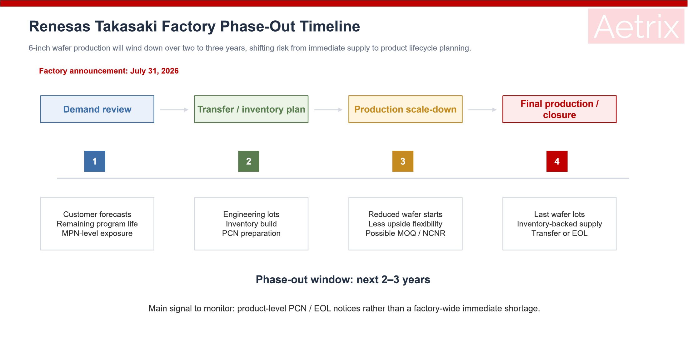
The initial phase is likely to center on demand collection. Renesas needs long-range forecasts to calculate how much inventory will be required and which products have enough future demand to justify a manufacturing transfer.
Customers may first see requests for extended forecast visibility, firm purchase commitments or confirmation of remaining program life. Factory production can continue normally during this stage, although unexpected increases in demand may become harder to accommodate once inventory plans are fixed.
The next phase will involve product routing decisions. Products selected for transfer may require new masks, engineering wafers, process matching, reliability testing and customer samples. Devices supported through final inventory will require advance wafer starts before Takasaki reduces production.
Supply flexibility generally declines during the final production stage. Remaining wafer capacity must cover last production lots, inventory builds and qualification activity. Selected products may then receive tighter order-acceptance rules, revised minimum quantities, NCNR conditions or fixed last-time-buy deadlines.
The strongest supply pressure is therefore more likely to appear near the end of the production window, particularly for products without an approved replacement wafer site.
| Transition Stage | Factory Activity | Likely Customer Signal | Supply Exposure |
|---|---|---|---|
| Demand review | Production continues while long-term demand is collected | Requests for forecasts and remaining program-life data | Lower |
| Transfer and inventory planning | Engineering lots, process qualification and advance wafer production | PCNs, sample requests and firmer purchase commitments | Low to moderate |
| Production scale-down | Fewer wafer starts and reduced scheduling flexibility | Longer planning windows, MOQ changes and tighter order acceptance | Moderate |
| Final production | Last wafer lots and final inventory preparation | Last-time-buy deadlines and NCNR orders | Higher for products without a transfer path |
| Post-closure supply | Transferred manufacturing or inventory-backed delivery | New lot traceability, finite inventory or EOL completion | MPN-specific |
What Products Are Linked to Takasaki?
Renesas' 2021 production strategy provides the clearest factory-level product classification. It listed Takasaki's existing main products as "PMOS" and "Analog," with IGBT identified as the site's focus device. In the same document, MCU production was assigned primarily to Naka, Saijo and Kawashiri. (Renesas, Production Strategy)
The "PMOS" label in the manufacturing strategy refers to Renesas' power MOSFET and switching-device activity. Public product records and engineering roles associated with Takasaki also connect the site with IGBT, FRD and MOSFET technology.
Current public disclosures support four principal product-risk categories:
- Selected legacy power MOSFET and switching devices
- Silicon IGBTs produced on mature wafer processes
- Fast-recovery diode and other power-diode dies
- Selected analog and mixed-signal ICs
These categories represent the strongest documented Takasaki exposure. Related parts within the same Renesas family can use different processes, wafer sites or manufacturing partners, so the category name alone cannot establish factory dependence.
Multi-die power products add another layer of complexity. The IGBT die and the internal fast-recovery diode may come from different front-end factories. Takasaki exposure can therefore apply to one semiconductor element inside a package while the remaining die and final assembly stay unchanged.
Product Risk Assessment for the Takasaki Phase-Out
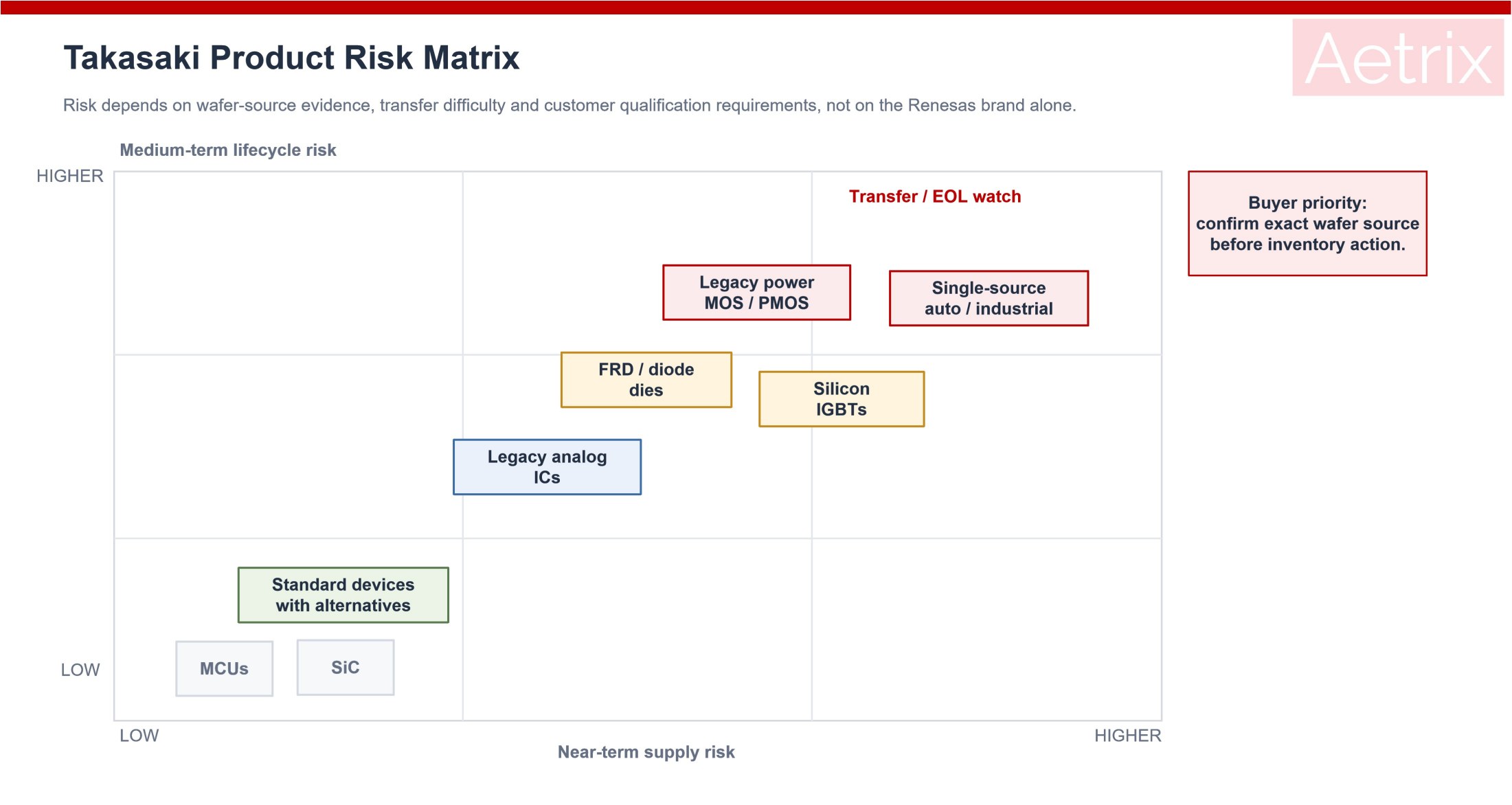
| Product Category | Public Evidence | Near-Term Supply Risk | Medium-Term Lifecycle Risk | Main Buyer Concern |
|---|---|---|---|---|
| Legacy power MOSFET and switching devices | PMOS listed as a main Takasaki product category | Low to moderate | Higher | Process-transfer economics and replacement availability |
| Silicon IGBTs | IGBT identified as a Takasaki focus device | Low to moderate | Higher | Transfer to a different wafer platform or eventual EOL |
| FRD and power-diode dies | Confirmed by a product-level Renesas PCN | Low to moderate | Higher | Qualification of an additional front-end site |
| Legacy analog and mixed-signal ICs | Analog listed as a main Takasaki category | Low to moderate | Moderate to higher | Parameter revalidation and manufacturing-site approval |
| Single-source automotive and industrial products | Requires exact MPN and wafer-site confirmation | Moderate | Higher | Long qualification and redesign cycle |
| Standard products with approved alternatives | Product-specific confirmation required | Lower | Moderate | Alternative qualification timing |
| RH850, RL78, RA and other MCU families | Main MCU production is assigned to other Renesas fabs | Low | Low | Verify manufacturing source before linking an MCU to Takasaki |
| SiC MOSFETs | Takasaki appeared in an earlier SiC manufacturing roadmap | Low from the current announcement | Product-strategy dependent | Wait for current product-level manufacturing disclosure |
Risk levels represent Aetrix Electronics' assessment based on disclosed factory categories, historical PCNs and expected process-transfer difficulty. They are separate from Renesas allocation, lead-time and EOL classifications.
Legacy Power Products Carry the Clearest Lifecycle Exposure
Mature power semiconductors remain active in appliances, industrial drives, power supplies, heating systems and automotive subsystems long after the original process platform was introduced.
Moving these products to another wafer factory requires detailed process matching. Breakdown voltage, on-state loss, switching speed, leakage, thermal performance and long-term reliability must remain within the approved product limits.
The transfer work can extend to epitaxial structure, trench geometry, junction termination, wafer thickness, backside metallization and die-attach compatibility. Each engineering change adds cost, qualification time and manufacturing risk.
Products with high shipment volume and several years of committed customer demand provide a stronger business case for migration. Low-volume devices, older package options and products with established alternatives are more likely to receive inventory-backed support or an EOL schedule.
Annual sales volume alone does not determine customer impact. A relatively small product can remain critical inside a long-lived industrial controller, medical platform or automotive module where redesign and certification require substantial time.
IGBT and FRD Exposure Can Differ Inside One Package
Renesas identified IGBT as a Takasaki focus device in its 2021 production strategy. The site also has documented links to fast-recovery diode production.
Many packaged IGBTs contain two semiconductor elements: the main IGBT die and a separate FRD die. Each die can use a different front-end wafer factory. A manufacturing change may therefore affect the diode source while leaving the IGBT die, package and external part number unchanged.
This structure makes die-level traceability important. Procurement records often capture the final assembly location but omit the front-end source of each internal die. Factory closure risk can remain hidden until a PCN identifies the affected element.
Confirmed Product Case: RJH65T14DPQ-A0#T0
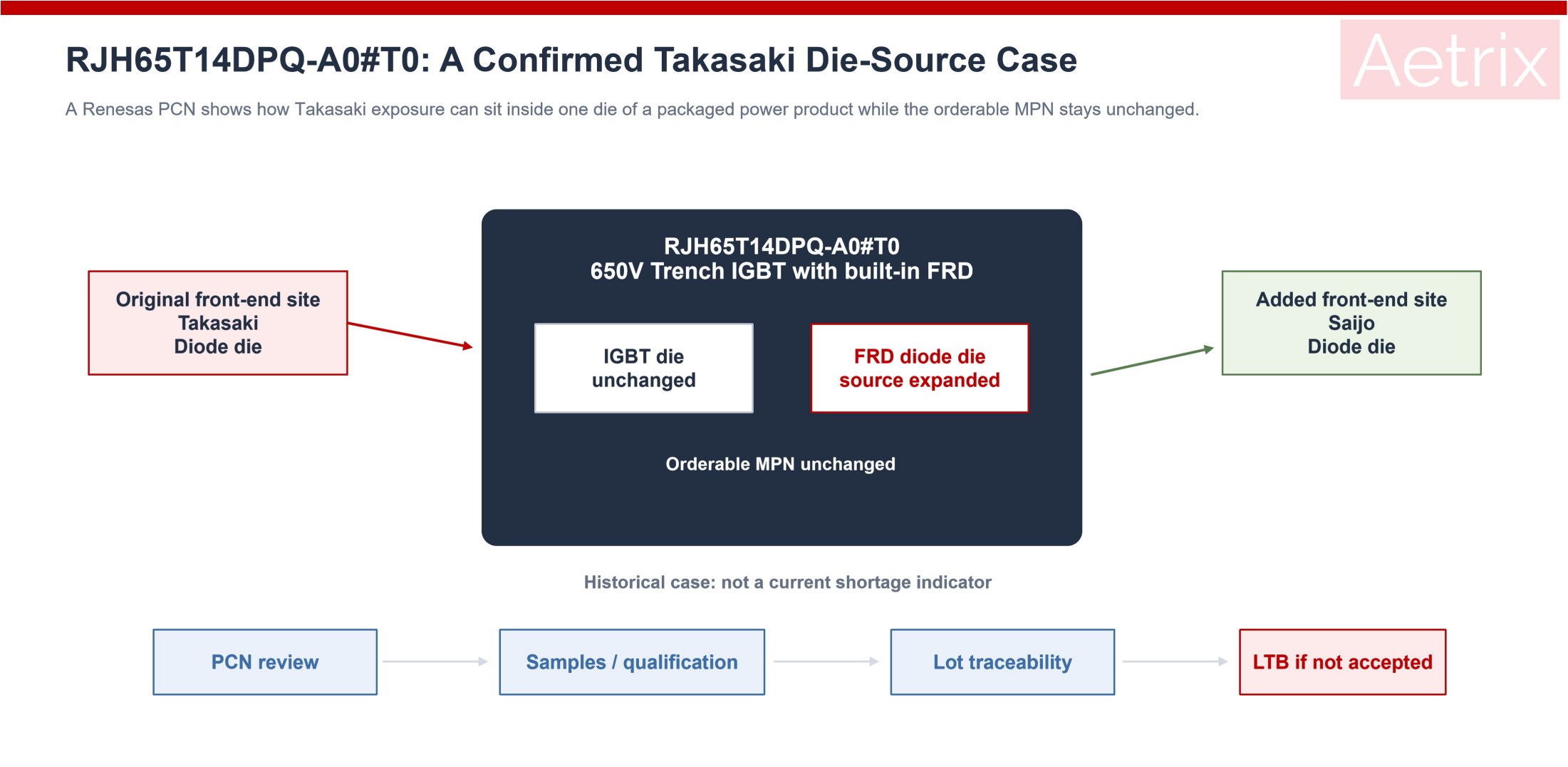
The clearest public example is RJH65T14DPQ-A0#T0, a 650V, 50A trench IGBT with a built-in fast-recovery diode in a TO-247A package. The product belongs to Renesas' 65T1x Series and was designed for induction-heating and microwave-oven applications. Renesas currently lists the part as obsolete. (Renesas, RJH65T14DPQ-A0#T0 Product Information)
A Renesas PCN published in November 2022 added Saijo as a front-end processing site for the product's diode die. Takasaki was the existing site. Renesas cited tight diode-die capacity at Takasaki as the reason for establishing the additional source.
The IGBT die remained unchanged. The orderable part number also stayed the same, and Renesas stated that the change had no impact on form, implementation, functionality, quality or reliability. Manufacturing-lot information on the label provided source traceability. Customers unable to accept the PCN were required to provide a last-time-buy demand and purchase order. (Renesas PCN BL202202489, Addition of Diode Die Front-End Factory)
| Item | RJH65T14DPQ-A0#T0 Case |
|---|---|
| Product type | 650V trench IGBT with built-in FRD |
| Series | 65T1x Series |
| Takasaki exposure | Diode-die front-end processing |
| Additional front-end site | Saijo |
| IGBT-die change | None |
| Orderable part number | Unchanged |
| Customer process | PCN review, qualification or last-time-buy decision |
| Current lifecycle status | Obsolete |
The part provides a historical manufacturing-transfer case rather than a current shortage indicator. It shows how Renesas can reduce Takasaki dependence by qualifying another front-end site for one internal die.
The same model may appear during the wider factory transition. An unchanged external MPN can still require technical review, sample evaluation, lot-traceability updates and formal customer approval.
Analog Products Have Broader but Less Visible Exposure
Analog was listed as a main Takasaki product category, although Renesas has not disclosed the associated series or orderable part numbers.
Current public records do not connect the company's full automotive PMIC, battery-management, sensor-interface, motor-driver or high-voltage analog portfolios with this factory. The relevant risk group consists of selected legacy analog and mixed-signal devices tied to Takasaki's 150mm process modules.
Analog process transfers can require more work than their mature geometry suggests. Bipolar devices, high-voltage structures, precision resistors, capacitors, isolation structures and metal systems all influence the final electrical distribution.
A receiving factory may reproduce the published limits while creating small shifts in offset, gain, noise, leakage, breakdown behavior or temperature drift. Automotive and industrial customers can require characterization data, reliability reports and production samples before approving the new manufacturing site.
Products with stable long-term demand have a stronger case for process migration. Older devices with low annual volume, narrow customer coverage or readily available replacements carry greater discontinuation exposure.
MCU and SiC Exposure
Renesas' main MCU production footprint is centered on other facilities. Its factory strategy assigns MCU production to sites including Naka, Saijo and Kawashiri. Current evidence places RH850, RL78, RA and other major MCU families outside the direct Takasaki risk group.
A direct Takasaki connection could still exist for an individual legacy device or internal die, so manufacturing-source confirmation remains appropriate for critical MPNs. The factory announcement itself does not indicate a broad change to Renesas automotive MCU supply.
Takasaki also appeared in Renesas' 2024 roadmap as a planned 6-inch manufacturing site for first-generation SiC products. The July 2026 announcement provides no current SiC product list or volume-production exposure. The direct closure assessment therefore remains focused on legacy silicon power and analog products with documented factory links.
Three Product Paths During the Factory Phase-Out
Renesas can use different lifecycle routes for different Takasaki products. The final decision will depend on remaining customer demand, technical migration difficulty, product profitability and the time required for qualification.
| Product Path | Best Fit | Customer Impact | Main Risk |
|---|---|---|---|
| Production transfer | Higher-volume products with long remaining demand | PCN review, samples, reliability qualification and manufacturing-site approval | Qualification delay or process-matching difficulty |
| Inventory-backed supply | Predictable demand with limited economic case for transfer | Long-term forecasts, firm commitments and possible NCNR orders | Finite supply after the final wafer run |
| Product discontinuation | Low-volume devices, old packages or products with established replacements | Last-time buy, alternative qualification or system redesign | Insufficient time to complete a replacement program |
Production transfer offers continued manufacturing but creates qualification work. The receiving factory may use different equipment, process controls or wafer dimensions, requiring Renesas to demonstrate equivalent performance and reliability.
Inventory-backed supply avoids an expensive process transfer for products with limited remaining life. Its success depends on accurate forecasts. Demand above the planned quantity becomes difficult to support after final wafer production ends.
Discontinuation is more likely where future revenue cannot justify transfer and inventory costs. Customers already holding an approved alternative will have greater flexibility than those operating a single-source design.
Takasaki's 150mm Exit and Kofu's 300mm Expansion
Renesas' broader power-semiconductor strategy provides important context for the Takasaki decision.
The company reopened its Kofu Factory in April 2024 as a dedicated 300mm power-semiconductor wafer fab following an investment of approximately ¥90 billion. Renesas said the facility would begin mass production of IGBTs and other products in 2025, with a product scope covering IGBTs, power MOSFETs and other power devices. (Renesas, Kofu 300mm Power Semiconductor Factory)
The two factories represent different manufacturing generations. Takasaki is an aging 150mm platform facing shrinking material and equipment support. Kofu is a 300mm platform intended to provide greater scale and efficiency for selected power-semiconductor products.
Kofu can support the future growth of Renesas' power business, while product compatibility will determine which Takasaki devices can migrate there. A 300mm power fab is optimized for particular device structures, process flows and production volumes. Some legacy analog and discrete products may require another Renesas site, an external foundry or a final inventory program.
At the corporate level, Renesas is shifting capital toward larger-wafer power production. At the product level, every Takasaki device still requires a separate lifecycle decision.
Part of Renesas' Longer 6-Inch Consolidation Strategy
The Takasaki phase-out continues a manufacturing restructuring that Renesas has pursued for more than a decade.
In 2018, the company announced plans to close the Yamaguchi Factory and consolidate the silicon production line at Shiga over approximately two to three years. Renesas stated that products made on the affected lines would either be transferred to other group facilities or discontinued. The decision followed a broader review of the company's 6-inch manufacturing footprint. (Renesas, Yamaguchi and Shiga Factory Consolidation Policy)
The historical sequence provides a practical guide to the Takasaki transition. A factory-level announcement is followed by product-level demand analysis, transfer decisions, PCNs, EOL notices and final production schedules. Different product groups move through the process at different times.
Customers can therefore expect Takasaki notifications to arrive in batches as Renesas determines the future of each process and MPN.
Buyer Priorities During the Takasaki Transition
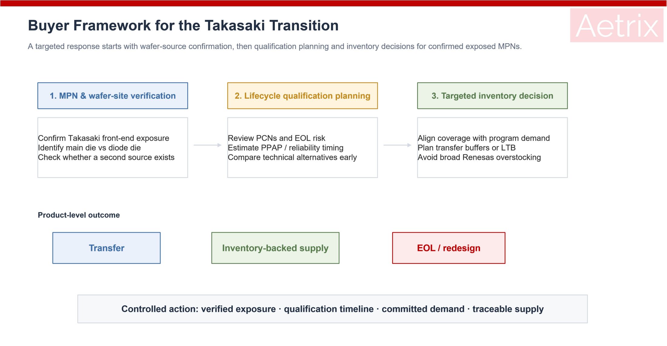
The first task is manufacturing-site verification. Renesas or an authorized sales channel should confirm whether each active analog or power MPN uses Takasaki front-end production, whether Takasaki manufactures the main die or an internal diode, and whether another qualified wafer source already exists.
The result should be recorded at the exact orderable-part-number level. Closely related products can use different processes, wafer sites and die configurations, making family-level assumptions unreliable.
Lifecycle planning should then focus on parts with long redesign and approval cycles. Automotive, industrial, medical and infrastructure customers may need time for PCN review, PPAP updates, reliability assessment, safety documentation, customer notification and system-level testing.
Alternative-product work is most effective before a fixed EOL deadline appears. Power-device comparisons need to cover voltage rating, continuous and pulsed current, conduction loss, switching energy, gate charge, diode behavior, thermal resistance, short-circuit capability and package compatibility.
Analog replacements require review of supply range, accuracy, offset, noise, transient response, protection functions, temperature performance, pinout and external-component requirements.
Inventory coverage should reflect confirmed Takasaki exposure, remaining program demand and alternative qualification time. A general increase across all Renesas analog and power inventory would consume working capital without addressing the actual factory-dependent MPNs.
Products selected for manufacturing transfer may require enough buffer stock to cover sample evaluation, customer approval and the production changeover. Products assigned to inventory-backed supply require clear agreement on demand commitments, NCNR terms, final order dates, storage responsibility and treatment of future upside demand.
What the Takasaki Exit Says About Mature-Node Manufacturing
The Takasaki closure highlights a supply-chain risk that receives less attention than demand cycles and factory utilization.
Mature semiconductor products are often viewed as stable because their designs, processes and end applications are well established. The physical manufacturing system supporting them can become increasingly fragile as equipment ages and the supplier base contracts.
Analog and power devices are particularly exposed to this mismatch. Their product lives often extend beyond those of digital processors, and customers expect consistent electrical performance over long production periods.
A shrinking 150mm ecosystem forces manufacturers to choose among process migration, lifetime inventory and product retirement. Each path transfers cost and risk differently. Process migration requires engineering and customer qualification. Lifetime inventory requires accurate forecasts and long-term storage. Product retirement shifts the redesign burden to the customer.
The transition also shows that factory closure and market withdrawal are separate decisions. Renesas is retaining analog and power R&D at Takasaki and investing in 300mm power manufacturing at Kofu. Its product strategy continues while the underlying manufacturing platform changes.
Other mature-node suppliers face similar decisions as older wafer lines approach practical end of life. Automotive and industrial customers will increasingly need to include wafer-platform age, single-site dependence and manufacturing-transfer readiness in BOM risk reviews.
Outlook
The Takasaki announcement creates limited near-term disruption and meaningful medium-term product-lifecycle exposure.
Renesas has provided a two-to-three-year transition period and plans to build inventory according to customer demand. The company has not announced a factory-wide allocation policy, a general price increase or a common lead-time extension.
Risk will develop unevenly. High-volume products may move to another factory. Devices with predictable but limited remaining demand may be supported through advance inventory. Low-volume products with expensive migration requirements may enter EOL.
Legacy power MOSFETs, switching devices, silicon IGBTs, power-diode dies and selected analog products deserve the closest review because public Renesas documents connect these categories with Takasaki.
The RJH65T14DPQ-A0#T0 PCN provides a useful example of the product-level detail involved. Takasaki produced the internal diode die, Saijo was added as another source, and the IGBT die and orderable part number remained unchanged.
The next important signals will come from manufacturing-site PCNs, EOL notices, requests for long-term demand commitments and product-specific qualification schedules. Buyers that identify Takasaki-dependent MPNs early will retain more time to evaluate transfers, build targeted inventory and approve alternatives.
Key Takeaways
- Renesas will phase out production at its Takasaki 6-inch wafer factory over the next two to three years.
- Aging equipment, utility infrastructure, discontinued materials and declining maintenance support are driving the decision.
- Renesas plans to build inventory based on customer demand before production ends.
- Historical factory documents connect Takasaki with power MOSFET and switching products, analog ICs, IGBTs and power-diode dies.
- Near-term supply exposure is limited, while medium-term lifecycle risk is higher for products tied to Takasaki-specific processes.
-
RJH65T14DPQ-A0#T0confirms a historical Takasaki diode-die connection and shows how an additional front-end site can be qualified without changing the orderable MPN. - Major Renesas MCU families are produced mainly at other front-end sites.
- Product outcomes are expected to include manufacturing transfer, inventory-backed supply and discontinuation.
- Single-source automotive and industrial products face the greatest qualification burden.
- Buyers should verify wafer sources at the exact MPN level, monitor PCNs and EOL notices, and align inventory with confirmed factory exposure.