
 My Inquiry
 My Account


Macronix MX29LV160DBTI-70G
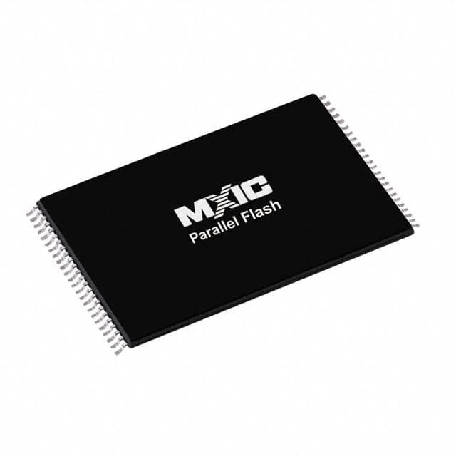
- Part No.:
- MX29LV160DBTI-70G
- Manufacturer:
- Macronix
- Category:
- Memory
- Package:
- 48-TFSOP (0.724", 18.40mm Width)
- Datasheet:
-
 MX29LV160DBTI-70G.pdf
- Description:
- IC FLASH 16MBIT PARALLEL 48TSOP
- Quantity:
- Payment:

- Shipping:

Inventory:8,115
Please send an inquiry. Send us your inquiry, and we will respond immediately.
Product details
Overview
MX29LV160DBTI-70G from Macronix is a 16Mbit parallel NOR Flash memory device designed for embedded code storage, boot memory, firmware storage, configuration data, and non-volatile program memory applications. The device supports byte/word mode operation, allowing organization as 2,097,152 × 8 or 1,048,576 × 16, and operates from a 2.7V to 3.6V supply range for 3V embedded systems.
As part of the Macronix MX29LV160D Flash memory family, MX29LV160DBTI-70G combines 70ns access time, JEDEC-compatible command operation, sector erase architecture, low-voltage write inhibit, sector protection, temporary sector unprotect, and a 48-pin TSOP package for mature embedded memory platforms. For engineers reviewing the MX29LV160DBTI-70G datasheet, MX29LV160DBTI-70G pinout, MX29LV160DBTI-70G application, or MX29LV160DBTI-70G equivalent, this device is widely used in boot ROM replacement, industrial controllers, communication equipment, consumer electronics, embedded firmware storage, and legacy parallel Flash memory designs.
Technical Context
In embedded systems, MX29LV160DBTI-70G operates as a parallel NOR Flash memory connected directly to a host processor, microcontroller, FPGA, or memory controller. Unlike raw NAND memory, NOR Flash supports random read access for code storage and execute-in-place style architectures where the system can fetch firmware or boot code directly from the memory array.
The MX29LV160D family supports byte/word mode selection, giving designers flexibility to use either an 8-bit or 16-bit memory bus. The device is organized as 16Mbit of non-volatile memory and uses sector-based erase operations, including boot-block sector organization for systems that need protected boot code and separately updateable application regions.
MX29LV160DBTI-70G is suitable for systems requiring stable 3V parallel Flash, JEDEC-compatible software command operation, 70ns read access, sector protection, in-system programming, and long-term firmware storage. It is commonly used in industrial boards, networking products, control systems, embedded instruments, printers, set-top boxes, and other platforms designed around asynchronous parallel NOR Flash.
Key Specifications
| Parameter | Value and Actual Design Meaning |
|---|---|
| Device Type | Parallel NOR Flash memory for embedded code and firmware storage. |
| Memory Size | 16Mbit total density for boot code, firmware images, configuration data, and program storage. |
| Memory Organization | 2,097,152 × 8 or 1,048,576 × 16, selected through byte/word mode operation. |
| Interface Type | Asynchronous parallel Flash interface compatible with standard memory-controller designs. |
| Supply Voltage | 2.7V to 3.6V operation for 3V embedded systems. |
| Access Time | 70ns speed grade supporting fast random read access for embedded firmware designs. |
| Sector Architecture | Boot-block sector structure with 16KB × 1, 8KB × 2, 32KB × 1, and 64KB × 31 sectors. |
| Protection Functions | Sector protect, chip unprotect, and temporary sector unprotect support controlled firmware updates. |
| Command Compatibility | JEDEC-compatible single-power-supply Flash command operation. |
| Write Protection | Low-VCC write inhibit helps prevent accidental program or erase during low-supply conditions. |
| Package | 48-pin TSOP package for standard surface-mount parallel NOR Flash layouts. |
| Temperature Range | Industrial temperature range, -40°C to +85°C. |
| Packaging | Tray packaging for production handling and assembly. |
Pinout & Package
The MX29LV160DBTI-70G pinout follows the 48-pin TSOP parallel NOR Flash package format. Key signals include address inputs, data I/O pins, chip enable, output enable, write enable, reset, ready/busy status, write-protect/accelerated-program support, byte/word mode selection, VCC, and ground pins.
For PCB implementation, the address and data buses should be routed with controlled timing skew and clean ground return. CE#, OE#, WE#, RESET#, and BYTE# control signals should be routed with attention to timing margins, while VCC decoupling capacitors should be placed close to the memory package to maintain stable read, program, and erase operation.
| Pin / Function | PCB Design and Circuit Role |
|---|---|
| A0–A19 | Address inputs used by the host controller to select memory locations and sector addresses. |
| DQ0–DQ14 | Bidirectional data bus pins used for x8 or x16 read, program, command, and status operations. |
| DQ15 / A-1 | Upper data bit in word mode or least-significant address input in byte mode. |
| CE# | Chip enable input used to select the Flash device for read, program, erase, and command cycles. |
| OE# | Output enable input controlling data output during read operations. |
| WE# | Write enable input used to latch command, address, and program data cycles. |
| RESET# | Hardware reset input used to return the device to read-array mode and support protection functions. |
| RY/BY# | Ready/busy output indicating internal program or erase operation status. |
| WP# / ACC | Write-protect and accelerated-program function pin depending on operating mode and voltage condition. |
| BYTE# | Byte/word mode selection input for x8 or x16 bus configuration. |
| VCC / GND | 3V supply and ground pins requiring stable decoupling and clean PCB return paths. |
| 48-Pin TSOP Package | Surface-mount memory package for parallel NOR Flash PCB layouts. |
Key Features
- 16Mbit parallel NOR Flash memory for boot and firmware storage.
- Byte/word selectable organization supports x8 and x16 host memory buses.
- 70ns access time supports fast asynchronous read operation.
- 2.7V to 3.6V supply range supports 3V embedded systems.
- Boot-block sector structure supports protected boot code and field firmware updates.
- Sector protect, chip unprotect, and temporary sector unprotect functions support update control.
- JEDEC-compatible software command operation supports standard Flash programming flows.
- Low-VCC write inhibit helps prevent unintended program or erase operations.
- RY/BY# output supports operation-completion monitoring.
- 48-pin TSOP package supports mature parallel Flash PCB footprints.
Applications
| Embedded Boot Memory | Industrial Controllers |
|---|---|
|
Use Scenario: Boot ROM replacement, firmware storage, bootloaders, and board startup code. Memory Role: MX29LV160DBTI-70G stores executable boot code and system firmware in non-volatile memory. Use Value: Supports random read access and mature parallel NOR boot architectures. |
Use Scenario: PLC modules, control boards, instrumentation systems, and industrial embedded platforms. Memory Role: Stores firmware images, calibration data, configuration tables, and field-update code. Use Value: Provides rugged 3V Flash storage with industrial temperature support. |
| Communication Equipment | Consumer & Legacy Embedded Systems |
|
Use Scenario: Routers, access equipment, network appliances, communication cards, and modem platforms. Memory Role: Provides parallel NOR storage for firmware, boot images, and device configuration. Use Value: Supports established memory-controller interfaces and direct code-read capability. |
Use Scenario: Printers, set-top boxes, appliances, handheld equipment, and existing parallel Flash designs. Memory Role: Replaces or supports legacy asynchronous NOR Flash storage requirements. Use Value: Helps maintain production continuity for systems built around 48-pin TSOP NOR Flash footprints. |
Equivalent & Alternatives
When evaluating MX29LV160DBTI-70G equivalent devices, engineers should compare memory density, x8/x16 organization, boot-block orientation, sector layout, access time, supply voltage, package footprint, command-set compatibility, CFI data, temperature grade, and programming algorithm behavior.
| Alternative Part | Technical Difference | Application Difference | Selection Advice |
|---|---|---|---|
| MX29LV160DTI-70G | Top-boot version of the same 16Mbit MX29LV160D family with different boot-block sector location. | Used when the firmware map expects boot sectors at the top of the address range. | Choose MX29LV160DBTI-70G when the target memory map requires bottom-boot sector organization. |
| MX29LV160CBTI-70G | Earlier compatible generation with different process revision and CFI data behavior compared with MX29LV160D. | Used in legacy systems already qualified with the MX29LV160C family. | Choose MX29LV160DBTI-70G for MX29LV160D qualification, added hardware write-protection, and accelerated program capability. |
| AM29LV160DB-70 | 16Mbit 3V parallel NOR Flash alternative with similar density and bottom-boot architecture but different manufacturer details. | Used in embedded boot memory and legacy NOR Flash designs. | Choose MX29LV160DBTI-70G when Macronix device ID, CFI behavior, and existing firmware qualification must be preserved. |
| S29AL016J70TFI020 | 16Mbit parallel NOR Flash alternative with different command behavior, timing, package, and manufacturer specifications. | Used in 3V asynchronous NOR Flash memory designs requiring similar density. | Choose MX29LV160DBTI-70G when the PCB, boot-block map, and software driver are already qualified for Macronix MX29LV160D. |
Compared with MX29LV160DTI-70G, MX29LV160DBTI-70G is optimized for designs requiring bottom-boot sector organization instead of top-boot placement. MX29LV160DBTI-70G vs AM29LV160DB-70 selection depends on device ID compatibility, CFI data, boot-block layout, programming algorithm support, package footprint, access-time margin, and existing firmware qualification.
Quality
MX29LV160DBTI-70G should be sourced as original Macronix components through traceable and controlled supply channels. Quality verification procedures may include package inspection, top-mark validation, solderability testing, device-ID reading, CFI-query verification, erase/program functional testing, sector-protection review, access-time validation, and incoming inspection according to embedded memory production requirements.
Because parallel NOR Flash often stores boot code or production firmware, reliability depends on correct firmware drivers, stable VCC during program and erase operations, sector-protection policy, write-inhibit behavior, address/data-bus signal integrity, and validated boot-block mapping. Traceable sourcing supports manufacturing quality and reduces counterfeit supply-chain risk, especially for long-life embedded platforms and legacy production programs.
Availability
MX29LV160DBTI-70G available at Aetrix Electronics and suitable for embedded boot memory, industrial controllers, communication equipment, consumer electronics, firmware storage, and legacy 3V parallel NOR Flash systems requiring stable component supply and repeatable production support.
Supply support may include scheduled delivery planning, volume procurement support, BOM continuity assistance, traceable sourcing management, and long-term availability support for OEM manufacturers, industrial-control developers, embedded-system designers, and electronics production programs.
For production deployment, confirming boot-block orientation, 48-pin TSOP footprint, 70ns access-time requirement, x8/x16 bus configuration, software command compatibility, and sourcing continuity helps reduce procurement risk and improve manufacturing stability.
Manufacturer
Macronix is a semiconductor manufacturer specializing in non-volatile memory technologies, including NOR Flash, NAND Flash, ROM, automotive memory, industrial memory, and embedded storage solutions for consumer, industrial, automotive, networking, and communication applications.
The Macronix parallel NOR Flash portfolio focuses on code storage, random read access, boot memory support, long-life embedded platforms, JEDEC-compatible command operation, sector protection, and package options for legacy and industrial memory designs.
FAQ
What is MX29LV160DBTI-70G used for?
MX29LV160DBTI-70G is used for embedded boot memory, firmware storage, configuration data, industrial controllers, communication equipment, consumer electronics, and legacy parallel NOR Flash memory systems.
Where can I find the MX29LV160DBTI-70G datasheet download?
The MX29LV160DBTI-70G datasheet is available from Macronix and includes memory organization, pin configuration, sector architecture, software command definitions, timing diagrams, electrical specifications, package data, and ordering information.
What should be considered in MX29LV160DBTI-70G PCB design?
PCB implementation should prioritize address/data-bus timing, stable VCC decoupling, clean CE#/OE#/WE# control routing, proper RESET# handling, BYTE# mode selection, and compatibility with the host processor or memory controller.
Is MX29LV160DBTI-70G a bottom-boot Flash device?
Yes. The "DB" ordering code identifies the bottom-boot version of the MX29LV160D family, making it suitable for systems where boot sectors are located at the bottom of the memory map.
What are common MX29LV160DBTI-70G equivalent solutions?
Common alternatives include MX29LV160DTI-70G, MX29LV160CBTI-70G, AM29LV160DB-70, and S29AL016J70TFI020 depending on boot-block orientation, command compatibility, device ID, access time, package footprint, and firmware qualification requirements.
MX29LV160DBTI-70G Specifications
- Product attributes
- Attribute value
- Manufacturer:
- Macronix
- Series:
- MX29LV
- Package/Case:
- 48-TFSOP (0.724", 18.40mm Width)
- Packaging:
- Tray
- Product Status:
- Active
- Programmable:
- Verified
- Memory Type:
- Non-Volatile
- Memory Format:
- FLASH
- Technology:
- FLASH - NOR
- Memory Size:
- 16Mbit
- Memory Organization:
- 2M x 8
- Memory Interface:
- Parallel
- Clock Frequency:
- -
- Write Cycle Time - Word, Page:
- 70ns
- Access Time:
- 70 ns
- Voltage - Supply:
- 2.7V ~ 3.6V
- Operating Temperature:
- -40°C ~ 85°C (TA)
- Grade:
- -
- Qualification:
- -
- Mounting Type:
- Surface Mount
- Supplier Device Package:
- 48-TSOP
MX29LV160DBTI-70G FAQ
1.How can I place an order for MX29LV160DBTI-70G through Aetrix?
Please submit a Request for Quotation (RFQ) for MX29LV160DBTI-70G on Aetrix. Our sales agent will provide a competitive quotation and guide you through the order confirmation once you accept the terms.
2.Are the price and stock information for MX29LV160DBTI-70G reliable?
The price and inventory of MX29LV160DBTI-70G are updated periodically and may fluctuate due to market conditions. Stock and pricing data are typically refreshed every 24 hours. Quotation validity for MX29LV160DBTI-70G is usually 5 days.
3.What payment methods are accepted for MX29LV160DBTI-70G?
We accept Wire Transfer, PayPal, Credit Card, Western Union, MoneyGram, and Escrow for MX29LV160DBTI-70G transactions.
Note: Certain payment methods may incur a processing fee.
4.How is shipping managed for MX29LV160DBTI-70G?
MX29LV160DBTI-70G orders can be shipped via leading logistics carriers, including DHL, UPS, FedEx, TNT, or Registered Mail.
Once your MX29LV160DBTI-70G order is processed, you will receive an email with the shipment details and tracking number.
Note: Tracking information may take up to 24 hours to appear. Express delivery typically takes 3–5 business days.
5.How can I obtain technical support or documentation for MX29LV160DBTI-70G?
For technical support, including MX29LV160DBTI-70G datasheets, pinout diagrams, or application guidance, please contact our engineering support team. They can provide detailed documentation and assistance for your MX29LV160DBTI-70G requirements.
6.How does Aetrix verify that MX29LV160DBTI-70G is sourced from the original manufacturer or authorized distributors?
All MX29LV160DBTI-70G products on Aetrix are procured from qualified distributors and authorized channels. Our dedicated quality assurance team conducts strict verification, including traceability checks and, if necessary, third-party testing. This ensures that MX29LV160DBTI-70G meets industry standards.
7.What is the process for return or replacement of MX29LV160DBTI-70G?
All MX29LV160DBTI-70G units undergo pre-shipment inspection (PSI). If there is an issue with MX29LV160DBTI-70G, returns or replacements are accepted under the following conditions:
1.Quantity discrepancies, incorrect items, or visible external defects (such as breakage or corrosion), acknowledged by Aetrix.
2.The issue is reported within 90 days of delivery.
3.The MX29LV160DBTI-70G part is unused and in its original packaging.
Return procedure for MX29LV160DBTI-70G:
1.Submit a request within 90 days.
2.Obtain a Return Material Authorization (RMA) from Aetrix.
MX29LV160DBTI-70G Tags

-
M24C02-WMN6TP
STMicroelectronics

-
AT24C02C-XHM-T
Microchip Technology

-
AT21CS01-STUM10-T
Microchip Technology

-
AT24C02C-SSHM-T
Microchip Technology

-
24LC01BT-I/OT
Microchip Technology

-
M24C02-FMC6TG
STMicroelectronics
-
AT24CS02-SSHM-T
Microchip Technology

-
93LC46BT-I/OT
Microchip Technology
-
AT24C04C-SSHM-T
Microchip Technology

-
24LC01BT-I/SN
Microchip Technology
-
24AA02UIDT-I/OT
Microchip Technology

-
AT24C08C-STUM-T
Microchip Technology
Tech Hub

Engineering guide to output capacitor selection for ASIC Vcore rails, covering bulk capacitors, polymer capacitors, MLCC decoupling, DC bias, ESR, ESL, placement, transient response and substitution ri…

Engineering guide to high-current ASIC Vcore rails, covering 12-phase buck architecture, PMBus control, dynamic load testing, output capacitor networks, smart power stage selection, thermal design and …

Voltage regulator guide covering linear, LDO, 7805, Zener, adjustable, buck, VRM and alternator regulators, with design checks, testing methods, troubleshooting and datasheet-based selection.

Amplifier guide covering voltage, current and power amplification, gain, feedback, amplifier classes, audio and RF applications, op-amp circuits, transimpedance amplifiers, datasheet selection and trou…

Machine vision system guide covering components, inspection workflow, camera and lens selection, FOV, pixel resolution, motion blur, strobe lighting, bandwidth, 2D/3D vision, integration, troubleshooti…

Electronic devices and circuits guide covering passive components, semiconductors, analog and digital circuits, circuit theory, practical calculations, troubleshooting, datasheet selection, and learnin…

Oil pressure sensor diagnosis covering symptoms, location, testing, replacement, socket access, common failure cases, and the electronic signal path between the pressure sensor, wiring, ECU and gauge s…

MLCC ESR, impedance and self-resonant frequency in decoupling networks. Covers PDN behavior, frequency response, measurement methods, failure cases and practical capacitor selection for power integrity…

An actuator converts a control signal and energy source into mechanical motion. This guide explains actuator types, working principles, electric and linear actuators, automotive use cases, troubleshoot…

A potentiometer is a three-terminal adjustable resistor used for voltage division, analog control, calibration and signal adjustment. This guide explains wiring, symbols, types, 10k values, digital pot…


