Nexperia USA Inc. 74HC138PW,112
- Part No.:
- 74HC138PW,112
- Manufacturer:
- Nexperia USA Inc.
- Category:
- Signal Switches, Multiplexers, Decoders
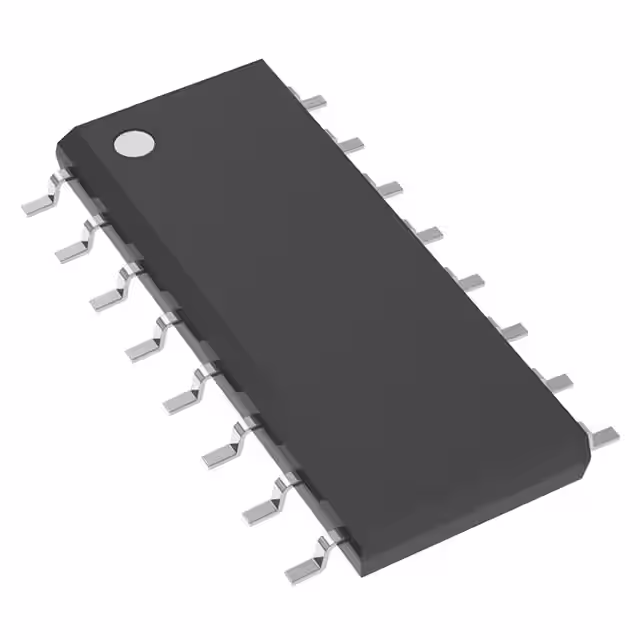
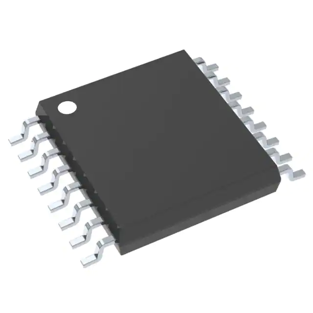
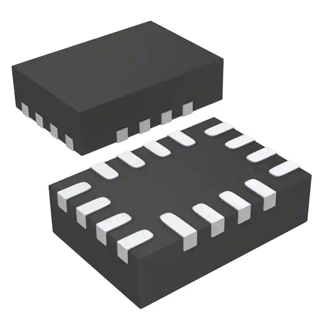
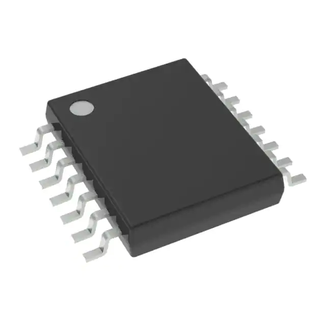
- Package:
- 16-TSSOP (0.173", 4.40mm Width)
- Datasheet:
-
 74HC138PW,112.pdf
- Description:
- IC DECODER/DEMUX 1X3:8 16TSSOP
- Quantity:
- Payment:

- Shipping:

Inventory:1,851
Please send an inquiry. Send us your inquiry, and we will respond immediately.
Product details
Overview
74HC138PW,112 from Nexperia USA Inc. is a high-speed CMOS 3-to-8 line decoder/demultiplexer with inverting outputs, designed for address decoding, memory chip-select generation, logic expansion, peripheral selection, and demultiplexing applications. The device decodes three binary weighted address inputs into eight mutually exclusive active-low outputs and is supplied in a compact 16-lead TSSOP package.
As part of the Nexperia 74HC logic portfolio, 74HC138PW,112 combines a 2.0V to 6.0V supply range, CMOS input levels, low power dissipation, high noise immunity, three enable inputs, active-low output decoding, and clamp-diode input protection for flexible digital logic integration. For engineers reviewing the 74HC138PW,112 datasheet, 74HC138PW,112 pinout, 74HC138PW,112 application, or 74HC138PW,112 equivalent, this device is widely used in memory address decoding, microcontroller peripheral selection, demultiplexer circuits, digital control logic, embedded systems, industrial boards, and general-purpose CMOS logic designs.
Technical Context
In digital systems, 74HC138PW,112 operates as a 1-of-8 decoder by translating the three address inputs A0, A1, and A2 into one selected active-low output among Y0 to Y7. All outputs remain HIGH unless E1 and E2 are LOW and E3 is HIGH, allowing the enable inputs to act as address-extension, strobe, or gating signals.
The device can also be used as an eight-output demultiplexer by applying data to one active-low enable input while using the remaining enable inputs as strobes. This makes the device useful in systems that need address-qualified signal routing, chip-select expansion, or logic steering without using programmable logic or multiple discrete gates.
74HC138PW,112 is the HC CMOS-input version of the 74HC/HCT138 family. Compared with the HCT version, it is intended for CMOS-level input thresholds across a wider 2.0V to 6.0V supply range, making it suitable for standard CMOS logic systems, low-voltage embedded boards, and 5V digital platforms where HC-level compatibility is required.
Key Specifications
| Parameter | Value and Actual Design Meaning |
|---|---|
| Device Type | 3-to-8 line decoder/demultiplexer with inverting active-low outputs. |
| Logic Family | 74HC high-speed CMOS logic with CMOS input-level compatibility. |
| Address Inputs | Three binary weighted address inputs: A0, A1, and A2. |
| Enable Inputs | Three enable inputs: E1 and E2 active LOW, E3 active HIGH. |
| Outputs | Eight mutually exclusive active-low outputs: Y0 to Y7. |
| Supply Voltage | 2.0V to 6.0V recommended operating range for 74HC138. |
| Output Current Capability | ±25mA absolute maximum output current rating per output pin; practical drive should follow datasheet operating limits. |
| Input Leakage Current | ±1.0µA maximum over temperature at VCC = 6.0V for low static input loading. |
| Input Capacitance | 3.5pF typical, supporting standard CMOS logic-interface loading. |
| ESD Protection | HBM class 2 above 2000V and CDM class C3 above 1000V. |
| Expansion Capability | Multiple enable inputs support expansion to a 1-of-32 decoder using four '138 ICs and one inverter. |
| Operating Temperature | -40°C to +125°C operating temperature range for broad industrial and embedded system use. |
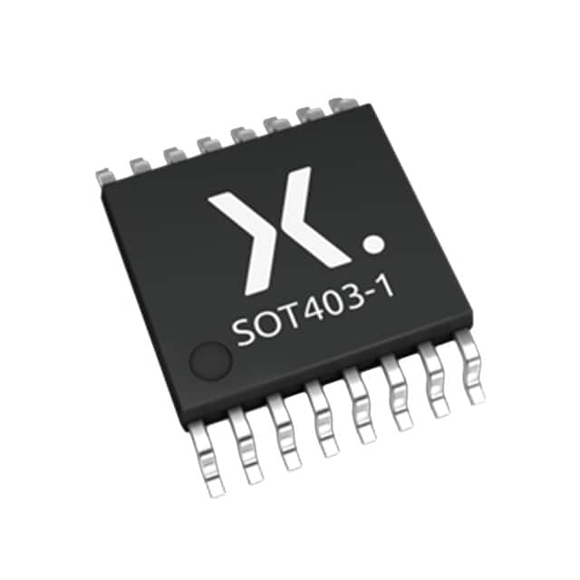
| Package | 16-lead TSSOP package, Nexperia PW package, SOT403-1. |
| Ordering Suffix | ",112" ordering suffix identifies Nexperia ordering and packing option for the 74HC138PW device. |
Pinout & Package
The 74HC138PW,112 pinout follows the standard 16-pin decoder layout in the TSSOP16 PW package. Address inputs A0, A1, and A2 are placed on pins 1 to 3, enable inputs E1, E2, and E3 on pins 4 to 6, output Y7 on pin 7, GND on pin 8, outputs Y6 to Y0 on pins 9 to 15, and VCC on pin 16.
For PCB implementation, VCC should be bypassed close to the package, address and enable inputs should be routed with clean logic edges, and output loading should remain within logic-family limits. Because the outputs are active LOW, downstream logic and memory chip-select polarity should be checked during schematic design.
| Pin / Function | PCB Design and Circuit Role |
|---|---|
| Pin 1 / A0 | Least significant address input used in output selection. |
| Pin 2 / A1 | Middle address input used in 3-bit decode logic. |
| Pin 3 / A2 | Most significant address input used in output selection. |
| Pin 4 / E1 | Active-low enable input; must be LOW for decoding to be active. |
| Pin 5 / E2 | Active-low enable input; must be LOW for decoding to be active. |
| Pin 6 / E3 | Active-high enable input; must be HIGH for decoding to be active. |
| Pin 7 / Y7 | Active-low decoded output for address selection state 7. |
| Pin 8 / GND | Ground reference for CMOS logic operation. |
| Pin 9 / Y6 | Active-low decoded output for address selection state 6. |
| Pin 10 / Y5 | Active-low decoded output for address selection state 5. |
| Pin 11 / Y4 | Active-low decoded output for address selection state 4. |
| Pin 12 / Y3 | Active-low decoded output for address selection state 3. |
| Pin 13 / Y2 | Active-low decoded output for address selection state 2. |
| Pin 14 / Y1 | Active-low decoded output for address selection state 1. |
| Pin 15 / Y0 | Active-low decoded output for address selection state 0. |
| Pin 16 / VCC | Positive supply pin for 2.0V to 6.0V HC logic operation. |
| TSSOP16 / SOT403-1 | Compact surface-mount package for dense logic and address-decoding layouts. |
Key Features
- 3-to-8 line decoder/demultiplexer with active-low mutually exclusive outputs.
- Three binary address inputs decode one of eight output lines.
- Three enable inputs support gating, cascading, and decoder expansion.
- Can be used as an eight-output demultiplexer with one enable input used as data input.
- Wide 2.0V to 6.0V operating supply range for CMOS logic systems.
- CMOS low power dissipation and high noise immunity.
- Input clamp diodes support interfacing through current-limiting resistors.
- Suitable for memory chip-select decoding and peripheral selection.
- HBM and CDM ESD protection support robust handling and assembly.
- 16-lead TSSOP package supports compact surface-mount PCB designs.
Applications
| Memory Address Decoding | Microcontroller Peripheral Selection |
|---|---|
|
Use Scenario: Memory-mapped systems, ROM/RAM chip-select generation, and address bus decoding. IC Role: 74HC138PW,112 converts address bits and enable strobes into one active-low chip-select output. Use Value: Simplifies memory-selection logic and reduces discrete-gate count. |
Use Scenario: MCU systems with multiple external peripherals or board-level logic blocks. IC Role: Generates individual active-low select signals from shared address or GPIO lines. Use Value: Expands controller selection capability without requiring extra programmable logic. |
| Demultiplexer Circuits | Industrial & Embedded Logic |
|
Use Scenario: Logic routing, data steering, scanned output control, and address-qualified signal distribution. IC Role: Uses enable and address inputs to route a logic condition to one of eight active-low outputs. Use Value: Provides simple hardware demultiplexing in standard CMOS logic systems. |
Use Scenario: Industrial boards, test fixtures, control panels, instrumentation, and embedded digital interfaces. IC Role: Implements deterministic decode logic for control, selection, and expansion functions. Use Value: Offers low-power, compact, and easy-to-qualify logic integration. |
Equivalent & Alternatives
When evaluating 74HC138PW,112 equivalent devices, engineers should compare logic family, input threshold type, supply-voltage range, package footprint, output polarity, propagation delay, temperature range, ESD rating, and pin-to-pin compatibility.
| Alternative Part | Technical Difference | Application Difference | Selection Advice |
|---|---|---|---|
| 74HCT138PW | Same decoder/demultiplexer function and TSSOP16 package family, but HCT input levels are intended for TTL-level compatibility at 5V operation. | Used when the driving logic provides TTL-compatible high-level signals rather than CMOS-level signals. | Choose 74HC138PW,112 when the system uses CMOS logic thresholds and a wider 2.0V to 6.0V supply range is required. |
| 74HC138D | Same 74HC138 logic function in a wider SO16 package instead of TSSOP16. | Used in designs requiring easier assembly, larger footprint, or existing SOIC layout compatibility. | Choose 74HC138PW,112 when the PCB is designed for the compact TSSOP16 / SOT403-1 footprint. |
| SN74HC138PWR | Texas Instruments 74HC logic-family equivalent with similar 3-to-8 decoder function and TSSOP packaging. | Used in similar CMOS address decoding and demultiplexer applications. | Choose 74HC138PW,112 when Nexperia qualification, ordering suffix, and existing BOM approval must be maintained. |
| MM74HC138MTC | onsemi/Fairchild HC decoder alternative with similar logic function but different manufacturer specifications and package details. | Used in general CMOS logic decoding and select-line generation circuits. | Choose 74HC138PW,112 when Nexperia pinout, package, and supply-chain continuity are preferred. |
Compared with 74HCT138PW, 74HC138PW,112 is optimized for CMOS-input logic systems and wider 2.0V to 6.0V operation rather than TTL-level 5V input compatibility. 74HC138PW,112 vs SN74HC138PWR selection depends on approved manufacturer list, timing margin, package footprint, logic-threshold requirements, ESD qualification, and sourcing continuity requirements.
Quality
74HC138PW,112 should be sourced as original Nexperia components through traceable and controlled supply channels. Quality verification procedures may include package inspection, top-mark validation, solderability testing, pin continuity checks, input threshold verification, functional truth-table testing, output-level measurement, and incoming inspection according to digital logic production requirements.
Because the device is often used for address decoding and chip-select generation, system reliability depends on correct enable polarity, stable supply decoupling, clean input timing, valid output loading, and confirmation that active-low outputs match the downstream logic. Traceable sourcing supports manufacturing quality and reduces counterfeit supply-chain risk for standard logic production programs.
Availability
74HC138PW,112 available at Aetrix Electronics and suitable for memory address decoding, peripheral chip-select generation, demultiplexer circuits, embedded digital logic, industrial control boards, communication modules, and general-purpose CMOS logic systems requiring stable component supply and repeatable production support.
Supply support may include scheduled delivery planning, volume procurement support, BOM continuity assistance, traceable sourcing management, and long-term availability support for OEM manufacturers, embedded-system developers, industrial-control designers, logic-board builders, and electronics production programs.
For production deployment, confirming logic family, supply voltage, input threshold compatibility, output polarity, package footprint, temperature range, and sourcing continuity helps reduce procurement risk and improve manufacturing stability.
Manufacturer
Nexperia USA Inc. is part of Nexperia, a semiconductor manufacturer specializing in standard logic, ESD protection devices, MOSFETs, bipolar transistors, diodes, analog switches, power discretes, and interface components for automotive, industrial, communication, computing, and consumer electronics.
The Nexperia standard logic portfolio focuses on CMOS logic families, compact package options, broad voltage support, low power dissipation, high noise immunity, automotive and industrial-grade availability, and long-term supply continuity for embedded logic, interface control, level-compatible systems, and board-level digital designs.
FAQ
What is 74HC138PW,112 used for?
74HC138PW,112 is used for 3-to-8 address decoding, memory chip-select generation, microcontroller peripheral selection, demultiplexing, logic expansion, and general-purpose CMOS digital control circuits.
Where can I find the 74HC138PW,112 datasheet download?
The 74HC138PW,112 datasheet is available from Nexperia and includes the functional diagram, pinout, truth table, operating conditions, static characteristics, switching specifications, package data, and application information.
What should be considered in 74HC138PW,112 PCB design?
PCB implementation should provide close VCC decoupling, clean address and enable routing, correct active-low output polarity, controlled output loading, and suitable grounding for reliable CMOS logic operation.
Are the outputs of 74HC138PW,112 active LOW?
Yes. 74HC138PW,112 has eight mutually exclusive active-low outputs. When the device is correctly enabled, one selected output goes LOW while the other outputs remain HIGH.
What are common 74HC138PW,112 equivalent solutions?
Common alternatives include 74HCT138PW, 74HC138D, SN74HC138PWR, and MM74HC138MTC depending on input threshold requirements, package footprint, supply voltage, timing, manufacturer approval, and sourcing continuity.
74HC138PW,112 Specifications
- Product attributes
- Attribute value
- Manufacturer:
- Nexperia USA Inc.
- Series:
- 74HC
- Package/Case:
- 16-TSSOP (0.173", 4.40mm Width)
- Packaging:
- Tube
- Product Status:
- Obsolete
- Type:
- Decoder/Demultiplexer
- Circuit:
- 1 x 3:8
- Independent Circuits:
- 1
- Current - Output High, Low:
- 5.2mA, 5.2mA
- Voltage Supply Source:
- Single Supply
- Voltage - Supply:
- 2V ~ 6V
- Operating Temperature:
- -40°C ~ 125°C
- Grade:
- -
- Qualification:
- -
- Mounting Type:
- Surface Mount
- Supplier Device Package:
- 16-TSSOP
74HC138PW,112 FAQ
1.How can I place an order for 74HC138PW,112 through Aetrix?
Please submit a Request for Quotation (RFQ) for 74HC138PW,112 on Aetrix. Our sales agent will provide a competitive quotation and guide you through the order confirmation once you accept the terms.
2.Are the price and stock information for 74HC138PW,112 reliable?
The price and inventory of 74HC138PW,112 are updated periodically and may fluctuate due to market conditions. Stock and pricing data are typically refreshed every 24 hours. Quotation validity for 74HC138PW,112 is usually 5 days.
3.What payment methods are accepted for 74HC138PW,112?
We accept Wire Transfer, PayPal, Credit Card, Western Union, MoneyGram, and Escrow for 74HC138PW,112 transactions.
Note: Certain payment methods may incur a processing fee.
4.How is shipping managed for 74HC138PW,112?
74HC138PW,112 orders can be shipped via leading logistics carriers, including DHL, UPS, FedEx, TNT, or Registered Mail.
Once your 74HC138PW,112 order is processed, you will receive an email with the shipment details and tracking number.
Note: Tracking information may take up to 24 hours to appear. Express delivery typically takes 3–5 business days.
5.How can I obtain technical support or documentation for 74HC138PW,112?
For technical support, including 74HC138PW,112 datasheets, pinout diagrams, or application guidance, please contact our engineering support team. They can provide detailed documentation and assistance for your 74HC138PW,112 requirements.
6.How does Aetrix verify that 74HC138PW,112 is sourced from the original manufacturer or authorized distributors?
All 74HC138PW,112 products on Aetrix are procured from qualified distributors and authorized channels. Our dedicated quality assurance team conducts strict verification, including traceability checks and, if necessary, third-party testing. This ensures that 74HC138PW,112 meets industry standards.
7.What is the process for return or replacement of 74HC138PW,112?
All 74HC138PW,112 units undergo pre-shipment inspection (PSI). If there is an issue with 74HC138PW,112, returns or replacements are accepted under the following conditions:
1.Quantity discrepancies, incorrect items, or visible external defects (such as breakage or corrosion), acknowledged by Aetrix.
2.The issue is reported within 90 days of delivery.
3.The 74HC138PW,112 part is unused and in its original packaging.
Return procedure for 74HC138PW,112:
1.Submit a request within 90 days.
2.Obtain a Return Material Authorization (RMA) from Aetrix.
74HC138PW,112 Tags
-
SN74HC138DR
Texas Instruments
-
TC7SB3157CFU,LF(CT
Toshiba Semiconductor and Storage
-
74CBTLV3257PW,118
Nexperia USA Inc.
-
SN74CBTLV3257PWR
Texas Instruments
-
74CBTLV3257GUX
Nexperia USA Inc.
-
74HC154BQ,118
Nexperia USA Inc.

-
P3S0200GMX
NXP USA Inc.
-
SN74CB3Q3245PWR
Texas Instruments
-
SN74CB3Q3257RGYR
Texas Instruments
-
TCA9543APWR
Texas Instruments
-
TCA9546APWR
Texas Instruments

-
SN74HC138N
Texas Instruments
Tech Hub
A decoder is an electronic circuit or integrated circuit that converts a coded input into a specific output state.
Use this kg to lbs converter to quickly convert kilograms to pounds or pounds to kilograms. It is useful for shipping weight, product specifications, package weight, material weight, equipment weight, …
Learn what analog devices are, including amplifiers, ADCs, DACs, sensors, voltage references, power ICs and ADI component selection for signal chain design.
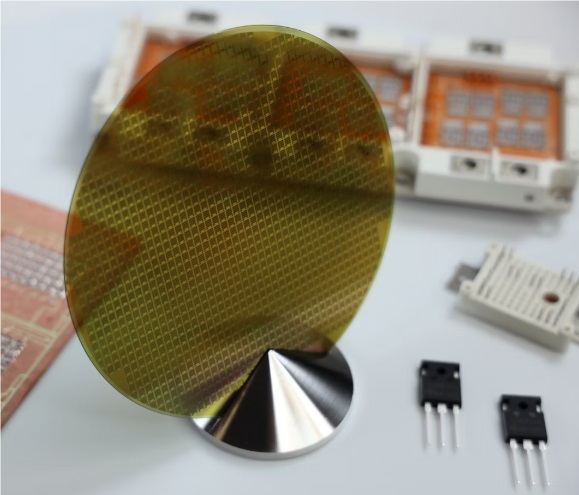
SiC, or silicon carbide, is a wide-bandgap semiconductor material used in high-efficiency power electronics.
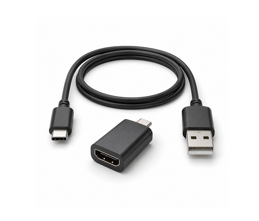
Type C, more formally called USB Type-C or USB-C, is a reversible connector used for charging, data transfer, display output, and accessory connection.
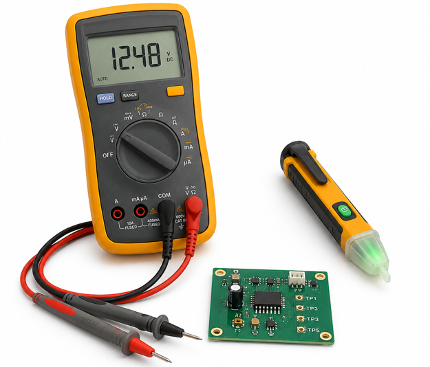
Voltage testing is a fundamental skill for electricians, engineers, technicians, and electronics hobbyists. Accurate voltage measurement ensures safe operation, prevents equipment damage, and verifies …
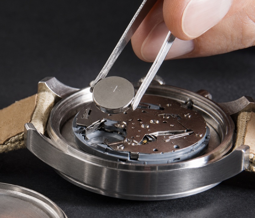
Find the correct SR626SW battery equivalent, including 377, AG4 and LR626 compatibility, silver oxide vs alkaline differences, size, voltage and watch replacement checks.
MLCCs are widely used in power supply circuits, DC-DC converters, decoupling networks, RF filters, automotive modules, industrial controllers, and high-density digital hardware. Their low ESR, compact …
MLCC damage is a common reliability problem in modern electronics, especially in compact PCB layouts, power supply circuits, automotive modules, industrial controllers, and high-density computing hardw…
Practical guide to understanding LDO dropout voltage, calculating input margin, and ensuring stable output regulation. Includes tips on battery-powered designs, load effects, and using the LDO Dropout …