
 My Inquiry
 My Account


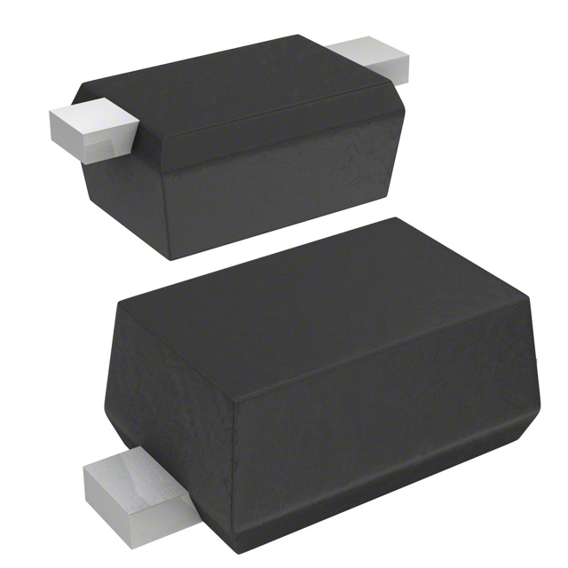
Infineon Technologies BBY5305WE6327
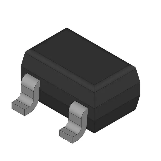
- Part No.:
- BBY5305WE6327
- Manufacturer:
- Infineon Technologies
- Package:
- SC-70, SOT-323
- Datasheet:
-
 BBY5305WE6327.pdf
- Description:
- VARIABLE CAPACITANCE DIODE
- Quantity:
- Payment:

- Shipping:

Inventory:6,719
Please send an inquiry. Send us your inquiry, and we will respond immediately.
Product details
Overview
BBY5305WE6327 from Infineon Technologies is a silicon hyperabrupt tuning diode configured as a common-cathode single diode in SCD80 package, with 1.4 pF capacitance at VR = 3 V, 2.6:1 capacitance ratio (CT1/CT3), and 0.47 Ω series resistance at 1 GHz - designed for low-voltage VCO tuning in mobile RF front-ends.
For engineers reviewing the BBY5305WE6327 datasheet, BBY5305WE6327 pinout, BBY5305WE6327 application, or BBY5305WE6327 equivalent, key selection criteria include tuning voltage range (0–6 V), temperature coefficient of capacitance (±10⁻⁴ /°C at VR = 2 V), reverse leakage (<10 nA at 4 V), and SCD80 thermal performance for compact RF module integration.
Technical Context
This hyperabrupt junction varactor delivers nonlinear C–V response optimized for wide tuning bandwidth in voltage-controlled oscillators, with CT ranging from 5.8 pF at 1 V to 3.1 pF at 3 V (f = 1 MHz). Its low rS (0.47 Ω typ.) minimizes phase noise contribution in resonant tank circuits.
The diode operates across –55 °C to +125 °C, with TCC varying from –4×10⁻⁴/°C to +10×10⁻⁴/°C depending on bias point, and exhibits <200 nA IR at 4 V and 85 °C - enabling stable frequency synthesis in thermally constrained handheld transceivers.
Key Specifications
| Parameter | Value and Actual Design Meaning |
|---|---|
| Capacitance @ 1 V | 5.8 pF max - sets low-end VCO frequency bound in 800–2200 MHz bands |
| Capacitance @ 3 V | 3.1 pF min - defines high-frequency limit and tuning linearity slope |
| Capacitance Ratio CT1/CT3 | 2.2 typ., 2.6 max - enables ≥15% fractional bandwidth in LC-tuned VCOs |
| Series Resistance rS | 0.47 Ω typ. @ 1 GHz - limits Q-factor degradation and phase noise floor |
| Reverse Voltage VR | 6 V max - supports rail-to-rail tuning with 3.3 V or 5 V DAC outputs |
| Reverse Current IR | ≤10 nA @ 4 V, 25 °C - ensures minimal DC loading on tuning control lines |
Pinout & Package
SCD80 (leadless, 2-terminal surface-mount) package with cathode-marked top-side laser marking; 0.7 mm × 1.45 mm footprint, 0.35 mm height, and thermal pad-compatible layout.
| Pin/Terminal | Circuit Role | Design Meaning |
|---|---|---|
| Anode | RF signal node | Connected to LC tank inductor; low rS preserves resonator Q |
| Cathode | DC bias reference | Common connection point for multiple diodes or ground-referenced tuning voltage |
Key Features
| Feature | Design Value |
|---|---|
| Hyperabrupt junction profile | Enables linearized frequency vs. voltage response in VCO tuning curves |
| Pb-free RoHS-compliant construction | Meets IPC-J-STD-020 moisture sensitivity level 1 (MSL1) for reflow compatibility |
| Low-temperature coefficient | TCC ≤ ±10⁻⁴ /°C near 2 V bias - reduces drift-induced frequency error over –40 to +85 °C |
| High Q factor at 1 GHz | Q > 100 derived from CT = 3.1 pF and rS = 0.47 Ω - critical for low-phase-noise oscillators |
Applications
| GSM/UMTS Transceiver VCO | Bluetooth LE Frequency Synthesizer |
|---|---|
Use Scenario: Dual-band VCO covering 900 MHz and 1900 MHz bands in mobile handset RFIC modules. IC Role / Device Role / Timing Role: Tuning element in Colpitts oscillator topology, biased via 3.3 V DAC output. Use Value: 2.6:1 CT ratio enables full band coverage without switched capacitor banks, reducing BOM count and PCB area. | Use Scenario: Channel-select VCO in Bluetooth 5.0 SoC with integrated PA and LNA. IC Role / Device Role / Timing Role: Varactor in 2.4 GHz LC tank, modulated by fast-settling 12-bit tuning voltage. Use Value: 0.47 Ω rS maintains oscillator Q > 80 at 2.4 GHz, limiting integrated phase noise to < –110 dBc/Hz (100 kHz offset). |
| Wi-Fi 2.4 GHz Local Oscillator | GPS L1 Band Front-End Tuning |
Use Scenario: Fixed-frequency LO generation in 802.11n WLAN transceivers with ±20 ppm stability requirement. IC Role / Device Role / Timing Role: Fine-tuning element trimming crystal oscillator harmonics or adjusting VCO center frequency post-calibration. Use Value: Low IR (<10 nA) prevents DAC output droop during long-duration calibration sequences, ensuring repeatable frequency alignment. | Use Scenario: Antenna matching network tuning in GPS/GLONASS dual-band active antennas. IC Role / Device Role / Timing Role: Bias-controlled reactance compensating for cable length and environmental dielectric shifts. Use Value: SCD80 package allows placement within 2 mm of antenna feed point, minimizing parasitic inductance that would degrade 1.575 GHz resonance accuracy. |
Equivalent & Alternatives
The following parts are listed as comparable options for similar tuning diode applications.
| Alternative Part | Technical Difference | Application Difference | Selection Advice |
|---|---|---|---|
| BBY58-02W | Higher CT (10.5 pF @ 1 V), lower CT ratio (1.9:1), same SCD80 package | Better suited for sub-1 GHz VCOs requiring larger capacitance swing | Select when target frequency range is below 1 GHz and higher absolute C is needed |
| SMV1232-011 | 0.35 Ω rS, 4.5 pF @ 1 V, SC79 package, higher VR (15 V) | Supports wider tuning voltage range and lower phase noise in high-performance synthesizers | Choose for >2 GHz designs where rS reduction outweighs footprint change |
Compared with BBY5305WE6327, BBY58-02W trades tuning linearity for extended low-frequency reach, while SMV1232-011 improves Q at the cost of larger package and higher bias voltage tolerance - making BBY5305WE6327 optimal for space-constrained 1–2.5 GHz mobile VCOs.
Availability
BBY5305WE6327 is available at Aetrix Electronics and suitable for GSM/UMTS transceiver VCOs, Bluetooth LE frequency synthesizers, Wi-Fi 2.4 GHz local oscillators, and GPS L1 band front-end tuning requiring stable component supply across automotive-grade temperature ranges.
Supply support for BBY5305WE6327 includes scheduled delivery planning, volume procurement assistance, BOM continuity management, traceable sourcing, and lifecycle availability coordination for OEM customers, industrial embedded developers, connected-device designers, and electronics production programs.
Manufacturer
Infineon Technologies is a German semiconductor manufacturer specializing in power management, RF, and automotive ICs, with leadership in silicon-based RF components for wireless infrastructure and mobile devices.
BBY5305WE6327 belongs to Infineon's BBY53 family of hyperabrupt tuning diodes, engineered specifically for low-voltage, high-linearity VCO tuning in battery-powered mobile communication equipment.
FAQ
What is the maximum reverse voltage rating for BBY5305WE6327?
The absolute maximum reverse voltage (VR) is 6 V at TA = 25 °C. Operation beyond this risks junction breakdown and irreversible capacitance shift. Derating is required above 25 °C per the datasheet's thermal curve - at 85 °C, VR must be limited to ≤4.8 V to maintain reliability over lifetime.
Does BBY5305WE6327 require a series current-limiting resistor in bias networks?
No external resistor is required for DC biasing because reverse leakage remains ≤10 nA at 4 V and 25 °C. However, a 10 kΩ isolation resistor is recommended between the DAC output and anode to suppress RF feedback into the control line, especially in high-gain VCO layouts where coupling may cause instability.
How does temperature affect capacitance stability in BBY5305WE6327?
At VR = 2 V, the temperature coefficient of capacitance (TCC) is –2.25×10⁻⁴ /°C, causing ∆CT ≈ –1.8% over –40 °C to +85 °C. This drift is compensated in closed-loop PLL systems via automatic frequency calibration (AFC), but open-loop VCOs require additional TCXO reference or digital lookup table correction.
Can BBY5305WE6327 be used in zero-bias (0 V VR) configurations?
Zero-bias operation is not recommended: at VR = 0 V, the junction is forward-biased under RF signal peaks, causing harmonic distortion and intermodulation. Minimum recommended VR is 0.5 V to ensure full depletion; typical designs use 1–3 V tuning range to balance linearity, capacitance swing, and noise performance.
BBY5305WE6327 Specifications
- Product attributes
- Attribute value
- Manufacturer:
- Infineon Technologies
- Series:
- -
- Package/Case:
- SC-70, SOT-323
- Packaging:
- Bulk
- Product Status:
- Active
- Capacitance @ Vr, F:
- 3.1pF @ 3V, 1MHz
- Capacitance Ratio:
- 2.6
- Capacitance Ratio Condition:
- C1/C3
- Voltage - Peak Reverse (Max):
- 6 V
- Diode Type:
- 1 Pair Common Cathode
- Q @ Vr, F:
- -
- Operating Temperature:
- -55°C ~ 125°C (TJ)
- Grade:
- -
- Qualification:
- -
- Mounting Type:
- Surface Mount
- Supplier Device Package:
- SOT-323
BBY5305WE6327 FAQ
1.How can I place an order for BBY5305WE6327 through Aetrix?
Please submit a Request for Quotation (RFQ) for BBY5305WE6327 on Aetrix. Our sales agent will provide a competitive quotation and guide you through the order confirmation once you accept the terms.
2.Are the price and stock information for BBY5305WE6327 reliable?
The price and inventory of BBY5305WE6327 are updated periodically and may fluctuate due to market conditions. Stock and pricing data are typically refreshed every 24 hours. Quotation validity for BBY5305WE6327 is usually 5 days.
3.What payment methods are accepted for BBY5305WE6327?
We accept Wire Transfer, PayPal, Credit Card, Western Union, MoneyGram, and Escrow for BBY5305WE6327 transactions.
Note: Certain payment methods may incur a processing fee.
4.How is shipping managed for BBY5305WE6327?
BBY5305WE6327 orders can be shipped via leading logistics carriers, including DHL, UPS, FedEx, TNT, or Registered Mail.
Once your BBY5305WE6327 order is processed, you will receive an email with the shipment details and tracking number.
Note: Tracking information may take up to 24 hours to appear. Express delivery typically takes 3–5 business days.
5.How can I obtain technical support or documentation for BBY5305WE6327?
For technical support, including BBY5305WE6327 datasheets, pinout diagrams, or application guidance, please contact our engineering support team. They can provide detailed documentation and assistance for your BBY5305WE6327 requirements.
6.How does Aetrix verify that BBY5305WE6327 is sourced from the original manufacturer or authorized distributors?
All BBY5305WE6327 products on Aetrix are procured from qualified distributors and authorized channels. Our dedicated quality assurance team conducts strict verification, including traceability checks and, if necessary, third-party testing. This ensures that BBY5305WE6327 meets industry standards.
7.What is the process for return or replacement of BBY5305WE6327?
All BBY5305WE6327 units undergo pre-shipment inspection (PSI). If there is an issue with BBY5305WE6327, returns or replacements are accepted under the following conditions:
1.Quantity discrepancies, incorrect items, or visible external defects (such as breakage or corrosion), acknowledged by Aetrix.
2.The issue is reported within 90 days of delivery.
3.The BBY5305WE6327 part is unused and in its original packaging.
Return procedure for BBY5305WE6327:
1.Submit a request within 90 days.
2.Obtain a Return Material Authorization (RMA) from Aetrix.
BBY5305WE6327 Tags
-
BBY5702VH6327XTSA1
Infineon Technologies
-
BBY5602VH6327XTSA1
Infineon Technologies
-
SMV1405-040LF
Skyworks Solutions Inc.
-
BBY6502VH6327XTSA1
Infineon Technologies
-
BBY6602VH6327XTSA1
Infineon Technologies
-
BBY5802VH6327XTSA1
Infineon Technologies
.jpg)
-
BB175X
NXP USA Inc.
-
SMV1430-040LF
Skyworks Solutions Inc.
-
SMV1273-079LF
Skyworks Solutions Inc.
-
SMV1255-079LF
Skyworks Solutions Inc.
-
SMV1213-079LF
Skyworks Solutions Inc.
-
SMV1247-079LF
Skyworks Solutions Inc.
Tech Hub

18650 battery guide covering lithium-ion cell basics, 3.6V/3.7V voltage, 4.2V charging, mAh and Wh capacity, protected cells, chargers, BMS, series-parallel packs, holders, welding and sourcing checks.…

Hall effect sensor guide covering working principle, linear and digital sensors, Arduino circuits, current sensing, speed detection, automotive applications, A3144 examples, signal filtering and datash…

Product Change Notification guide for electronic components, covering PCN meaning, PCN vs PDN/EOL, common change types, risk levels, form-fit-function review, engineering validation, BOM control, LTB/L…

A practical guide to blend door actuators, covering HVAC function, symptoms, location, AC and heater issues, reset and calibration, replacement cost, electrical diagnosis, compatibility checks, and rep…

Engineering guide to Raspberry Pi alternatives, covering chip-level differences, Orange Pi, ROCK, Jetson, Banana Pi, NanoPi, Compute Module, Pico, GPIO, camera, HAT compatibility, and replacement risks…

Engineering guide to dynamic load response testing for high-current buck converters, covering load step setup, slew rate, Vcore undershoot, overshoot, recovery time, probe location, output capacitors a…

Engineering guide to output capacitor selection for ASIC Vcore rails, covering bulk capacitors, polymer capacitors, MLCC decoupling, DC bias, ESR, ESL, placement, transient response and substitution ri…

Engineering guide to high-current ASIC Vcore rails, covering 12-phase buck architecture, PMBus control, dynamic load testing, output capacitor networks, smart power stage selection, thermal design and …

Voltage regulator guide covering linear, LDO, 7805, Zener, adjustable, buck, VRM and alternator regulators, with design checks, testing methods, troubleshooting and datasheet-based selection.

Amplifier guide covering voltage, current and power amplification, gain, feedback, amplifier classes, audio and RF applications, op-amp circuits, transimpedance amplifiers, datasheet selection and trou…


