
 My Inquiry
 My Account


Cypress Semiconductor Corp CY62136FV30LL-45ZSXA
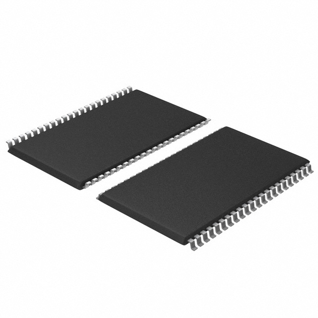
- Part No.:
- CY62136FV30LL-45ZSXA
- Manufacturer:
- Cypress Semiconductor Corp
- Category:
- Memory
- Package:
- 44-TSOP (0.400", 10.16mm Width)
- Datasheet:
-
 CY62136FV30LL-45ZSXA.pdf
- Description:
- IC SRAM 2MBIT PARALLEL 44TSOP II
- Quantity:
- Payment:

- Shipping:

Inventory:2,130
Please send an inquiry. Send us your inquiry, and we will respond immediately.
Product details
Overview
CY62136FV30LL-45ZSXA from Cypress Semiconductor is a 2-Mbit (128 K × 16) CMOS static RAM with 45 ns access time, 2.2–3.6 V supply range, and ultra-low standby current (1 µA typical). It operates across –40 °C to +85 °C (Industrial/Auto-A grade) and uses byte-wide I/O control via BHE/ BLE for efficient memory expansion in portable embedded systems.
For engineers reviewing the CY62136FV30LL-45ZSXA datasheet, CY62136FV30LL-45ZSXA pinout, CY62136FV30LL-45ZSXA application, or CY62136FV30LL-45ZSXA equivalent, key selection criteria include its MoBL® low-power architecture, VFBGA/TSOP II package compatibility, automatic CE power-down behavior, and pin-level interoperability with CY62136V and CY62136EV30 series.
Technical Context
This SRAM implements a 128K × 16-bit array with independent high- and low-byte enables (BHE/BLE), enabling selective 8-bit writes without read-modify-write cycles. Its CMOS design delivers deterministic timing under varying VCC (2.2–3.6 V) and temperature (–40 °C to +85 °C), with guaranteed tRC = 45 ns and tAA = 45 ns at VCC = 3.0 V.
The device supports three power states: active (ICC ≤ 18 mA max), automatic CE power-down (ISB1 ≤ 5 µA), and data retention (ICCDR ≤ 4 µA at VCC = 1.5 V). Output tristate control is managed by CE, OE, BHE, and BLE - all inputs must meet CMOS voltage thresholds to guarantee ISB1/ISB2 compliance.
Key Specifications
| Parameter | Value and Actual Design Meaning |
|---|---|
| Memory Organization | 128 K × 16-bit (2 Mbit); enables 16-bit data bus interface without external multiplexing |
| Access Time (tAA) | 45 ns max; ensures reliable read timing at 22 MHz system clock with setup/hold margin |
| Supply Voltage Range | 2.2 V to 3.6 V; compatible with Li-ion battery discharge profile and 3.3 V logic rails |
| Standby Current (ISB2) | 5 µA max (Industrial); reduces system quiescent power by >99% when deselected (CE HIGH) |
| Active Current (ICC) | 18 mA max at fmax; scales linearly with frequency for predictable power budgeting |
| Operating Temperature | –40 °C to +85 °C; qualified for industrial and automotive-A environments per AEC-Q100 stress profiles |
| Data Retention Voltage | 1.5 V min; allows backup operation during brown-out or battery switchover without data loss |
Pinout & Package
Package: 48-ball VFBGA (6 mm × 8 mm, 0.5 mm pitch), RoHS-compliant, thermal resistance θJA = 75 °C/W (still air).
| Pin/Terminal | Circuit Role | Design Meaning |
|---|---|---|
| A0–A16 | Address Inputs | 17-bit address bus supporting full 128K-word addressing; A16 enables 256K-word expansion mode |
| I/O0–I/O7 | Low-Byte Data I/O | Bi-directional 8-bit data path enabled only when BLE = LOW; high-impedance when deselected |
| I/O8–I/O15 | High-Byte Data I/O | Bi-directional 8-bit data path enabled only when BHE = LOW; isolated from low-byte during partial writes |
| CE | Chip Enable | Primary device select; forces automatic power-down and high-Z outputs when HIGH |
| OE | Output Enable | Controls output drivers only; does not affect power state unless CE is also LOW |
| WE | Write Enable | Active-LOW write strobe; initiates write when CE and BHE/BLE are concurrently LOW |
| BLE / BHE | Byte Low/High Enable | Independent 8-bit write gating; enables true byte-write capability without read-modify-write overhead |
| VCC / VSS | Power / Ground | Dual VCC pins improve noise immunity; two VSS pins reduce ground bounce in high-speed operation |
Key Features
| Feature | Design Value |
|---|---|
| MoBL® Ultra-Low Power Architecture | 1 µA typical standby current enables multi-week battery life in always-on sensor nodes |
| Automatic CE Power-Down | Reduces ICC by >90% when addresses stall, eliminating need for external power-gating logic |
| Byte-Enable Write Control | Eliminates read-modify-write cycles for 8-bit updates, cutting write latency by up to 40% |
| Pb-Free VFBGA & TSOP II Packages | 48-ball VFBGA (6 × 8 mm) supports high-density PCB layouts; pin-compatible with legacy TSOP II footprints |
| Guaranteed Data Retention at 1.5 V | Maintains stored data during brown-out events or backup battery transitions without external capacitor hold-up |
Applications
| Wireless Sensor Node Memory | Automotive Telematics Buffer |
|---|---|
Use Scenario: Battery-powered environmental sensor collecting temperature/humidity every 5 seconds and buffering 10 minutes of data before transmission. IC Role / Device Role / Timing Role: Non-volatile buffer storing timestamped samples; accessed randomly for burst upload; requires sub-µA sleep current and fast wake-up. Use Value: 1 µA ISB2 enables >3-month battery life on CR2032; 45 ns tAA supports real-time logging at 20 kSPS without FIFO overflow. | Use Scenario: CAN-based vehicle diagnostics module capturing ECU fault codes and live PID streams during ignition-off periods. IC Role / Device Role / Timing Role: Volatile scratchpad for transient diagnostic data; powered from backup rail during key-off; retains content down to 1.5 V. Use Value: VDR = 1.5 V allows retention during 12 V battery sag to 9 V; BHE/BLE enables selective logging of high-priority DTCs without corrupting active session data. |
| Industrial HMI Display Frame Buffer | Portable Medical Device Data Cache |
Use Scenario: Touch-enabled factory HMI with 480×272 RGB display requiring double-buffered graphics to prevent tearing during UI animation. IC Role / Device Role / Timing Role: Dual-port frame buffer holding front/back buffers; accessed sequentially by GPU and asynchronously by CPU for UI updates. Use Value: 128K × 16 organization provides exact 480×272×16-bit buffer space; 45 ns tAA sustains 60 Hz refresh with <1% CPU overhead. | Use Scenario: Handheld ECG monitor acquiring 12-lead signals at 1 kHz, compressing and caching 30 seconds before Bluetooth transfer. IC Role / Device Role / Timing Role: High-reliability temporary storage for raw waveform data; must survive brief power interruptions during battery swap. Use Value: Data retention at 1.5 V ensures no waveform loss during hot-swap; low ICC (1.6 mA typ @ 1 MHz) extends single-charge runtime to >8 hours. |
Equivalent & Alternatives
The following parts are listed as comparable options for similar SRAM applications.
| Alternative Part | Technical Difference | Application Difference | Selection Advice |
|---|---|---|---|
| ISSI IS62WV12816BLL-45NLI | Same 128K × 16 organization, 45 ns speed, and 2.2–3.6 V range; but uses standard 44-pin TSOP II only (no VFBGA option) | Lacks VFBGA footprint; higher θJA (77 °C/W) limits thermal headroom in sealed enclosures | Select when board layout rework for TSOP II is acceptable and VFBGA assembly capability is unavailable |
| ON Semiconductor NVSRAM NVTFS25616LDE | Non-volatile variant with integrated EEPROM backup; 55 ns access; 2.7–3.6 V only; no 2.2 V support | Provides automatic data retention on power loss but adds 100 µs save latency and higher cost | Select only if guaranteed non-volatility during unexpected shutdown is mandatory and 55 ns timing is acceptable |
Compared with IS62WV12816BLL-45NLI and NVTFS25616LDE, CY62136FV30LL-45ZSXA uniquely balances ultra-low standby power (1 µA), VFBGA density, and full 2.2–3.6 V operation - making it optimal for space-constrained, battery-sensitive designs where true volatility is acceptable and voltage flexibility is critical.
Availability
CY62136FV30LL-45ZSXA is available at Aetrix Electronics and suitable for wireless sensor nodes, automotive telematics modules, industrial HMIs, and portable medical devices requiring stable component supply across extended temperature ranges and long production lifecycles.
Supply support for CY62136FV30LL-45ZSXA includes scheduled delivery planning, volume procurement assistance, BOM continuity management, traceable sourcing, and lifecycle availability coordination for OEM customers, industrial embedded developers, connected-device designers, and electronics production programs.
Manufacturer
Cypress Semiconductor (now part of Infineon Technologies) designs high-performance memory and microcontroller solutions for embedded, automotive, and industrial applications, with emphasis on low-power innovation and reliability.
The CY62136FV30 belongs to the MoBL® (More Battery Life) SRAM product line, engineered specifically for portable and energy-harvesting systems where sub-microamp standby current and rapid wake-up from deep sleep are essential design requirements.
FAQ
What is the minimum VCC required to retain data in CY62136FV30LL-45ZSXA?
The device guarantees data retention down to VCC = 1.5 V, as specified in the Data Retention Characteristics table. At this voltage, ICCDR remains ≤ 4 µA under Industrial/Auto-A conditions. This enables operation during brown-out events or battery sag without data loss, provided CE and byte enables are held at valid CMOS levels.
Does CY62136FV30LL-45ZSXA support true 8-bit writes without read-modify-write?
Yes. Independent Byte High Enable (BHE) and Byte Low Enable (BLE) inputs allow selective activation of I/O8–I/O15 or I/O0–I/O7 during write cycles. When only one byte enable is asserted LOW while CE and WE are active, only that 8-bit segment is updated - eliminating read-modify-write overhead and reducing write latency by up to 40%.
Can CY62136FV30LL-45ZSXA be used in automotive applications beyond AEC-Q100 Grade 2?
Yes. The CY62136FV30LL variant is qualified for Automotive-E grade (–40 °C to +125 °C), exceeding AEC-Q100 Grade 2 (–40 °C to +105 °C) requirements. Its ISB2 ≤ 20 µA and tRC = 55 ns at +125 °C make it suitable for under-hood telematics and ADAS subsystems where extended temperature operation is mandatory.
How does automatic CE power-down differ from standard standby mode?
Automatic CE power-down activates when CE is HIGH *and* address lines are static (no toggling), reducing ICC by >90% compared to active mode. Standard standby (CE HIGH, dynamic addresses) draws slightly more current. Both modes place I/Os in high-Z, but only automatic power-down leverages internal address monitoring to gate internal clocks - a feature absent in basic SRAMs.
CY62136FV30LL-45ZSXA Specifications
- Product attributes
- Attribute value
- Manufacturer:
- Cypress Semiconductor Corp
- Series:
- MOBL™
- Package/Case:
- 44-TSOP (0.400", 10.16mm Width)
- Packaging:
- Bulk
- Product Status:
- Active
- Programmable:
- Not Verified
- Memory Type:
- Volatile
- Memory Format:
- SRAM
- Technology:
- SRAM - Asynchronous
- Memory Size:
- 2Mbit
- Memory Organization:
- 128K x 16
- Memory Interface:
- Parallel
- Clock Frequency:
- -
- Write Cycle Time - Word, Page:
- 45ns
- Access Time:
- 45 ns
- Voltage - Supply:
- 2.2V ~ 3.6V
- Operating Temperature:
- -40°C ~ 85°C (TA)
- Grade:
- -
- Qualification:
- -
- Mounting Type:
- Surface Mount
- Supplier Device Package:
- 44-TSOP II
CY62136FV30LL-45ZSXA FAQ
1.How can I place an order for CY62136FV30LL-45ZSXA through Aetrix?
Please submit a Request for Quotation (RFQ) for CY62136FV30LL-45ZSXA on Aetrix. Our sales agent will provide a competitive quotation and guide you through the order confirmation once you accept the terms.
2.Are the price and stock information for CY62136FV30LL-45ZSXA reliable?
The price and inventory of CY62136FV30LL-45ZSXA are updated periodically and may fluctuate due to market conditions. Stock and pricing data are typically refreshed every 24 hours. Quotation validity for CY62136FV30LL-45ZSXA is usually 5 days.
3.What payment methods are accepted for CY62136FV30LL-45ZSXA?
We accept Wire Transfer, PayPal, Credit Card, Western Union, MoneyGram, and Escrow for CY62136FV30LL-45ZSXA transactions.
Note: Certain payment methods may incur a processing fee.
4.How is shipping managed for CY62136FV30LL-45ZSXA?
CY62136FV30LL-45ZSXA orders can be shipped via leading logistics carriers, including DHL, UPS, FedEx, TNT, or Registered Mail.
Once your CY62136FV30LL-45ZSXA order is processed, you will receive an email with the shipment details and tracking number.
Note: Tracking information may take up to 24 hours to appear. Express delivery typically takes 3–5 business days.
5.How can I obtain technical support or documentation for CY62136FV30LL-45ZSXA?
For technical support, including CY62136FV30LL-45ZSXA datasheets, pinout diagrams, or application guidance, please contact our engineering support team. They can provide detailed documentation and assistance for your CY62136FV30LL-45ZSXA requirements.
6.How does Aetrix verify that CY62136FV30LL-45ZSXA is sourced from the original manufacturer or authorized distributors?
All CY62136FV30LL-45ZSXA products on Aetrix are procured from qualified distributors and authorized channels. Our dedicated quality assurance team conducts strict verification, including traceability checks and, if necessary, third-party testing. This ensures that CY62136FV30LL-45ZSXA meets industry standards.
7.What is the process for return or replacement of CY62136FV30LL-45ZSXA?
All CY62136FV30LL-45ZSXA units undergo pre-shipment inspection (PSI). If there is an issue with CY62136FV30LL-45ZSXA, returns or replacements are accepted under the following conditions:
1.Quantity discrepancies, incorrect items, or visible external defects (such as breakage or corrosion), acknowledged by Aetrix.
2.The issue is reported within 90 days of delivery.
3.The CY62136FV30LL-45ZSXA part is unused and in its original packaging.
Return procedure for CY62136FV30LL-45ZSXA:
1.Submit a request within 90 days.
2.Obtain a Return Material Authorization (RMA) from Aetrix.
CY62136FV30LL-45ZSXA Tags

-
M24C02-WMN6TP
STMicroelectronics

-
AT24C02C-XHM-T
Microchip Technology

-
AT21CS01-STUM10-T
Microchip Technology

-
AT24C02C-SSHM-T
Microchip Technology

-
24LC01BT-I/OT
Microchip Technology

-
M24C02-FMC6TG
STMicroelectronics
-
AT24CS02-SSHM-T
Microchip Technology

-
93LC46BT-I/OT
Microchip Technology
-
AT24C04C-SSHM-T
Microchip Technology

-
24LC01BT-I/SN
Microchip Technology
-
24AA02UIDT-I/OT
Microchip Technology

-
AT24C08C-STUM-T
Microchip Technology
Tech Hub

Hall effect sensor guide covering working principle, linear and digital sensors, Arduino circuits, current sensing, speed detection, automotive applications, A3144 examples, signal filtering and datash…

Product Change Notification guide for electronic components, covering PCN meaning, PCN vs PDN/EOL, common change types, risk levels, form-fit-function review, engineering validation, BOM control, LTB/L…

A practical guide to blend door actuators, covering HVAC function, symptoms, location, AC and heater issues, reset and calibration, replacement cost, electrical diagnosis, compatibility checks, and rep…

Engineering guide to Raspberry Pi alternatives, covering chip-level differences, Orange Pi, ROCK, Jetson, Banana Pi, NanoPi, Compute Module, Pico, GPIO, camera, HAT compatibility, and replacement risks…

Engineering guide to dynamic load response testing for high-current buck converters, covering load step setup, slew rate, Vcore undershoot, overshoot, recovery time, probe location, output capacitors a…

Engineering guide to output capacitor selection for ASIC Vcore rails, covering bulk capacitors, polymer capacitors, MLCC decoupling, DC bias, ESR, ESL, placement, transient response and substitution ri…

Engineering guide to high-current ASIC Vcore rails, covering 12-phase buck architecture, PMBus control, dynamic load testing, output capacitor networks, smart power stage selection, thermal design and …

Voltage regulator guide covering linear, LDO, 7805, Zener, adjustable, buck, VRM and alternator regulators, with design checks, testing methods, troubleshooting and datasheet-based selection.

Amplifier guide covering voltage, current and power amplification, gain, feedback, amplifier classes, audio and RF applications, op-amp circuits, transimpedance amplifiers, datasheet selection and trou…

Machine vision system guide covering components, inspection workflow, camera and lens selection, FOV, pixel resolution, motion blur, strobe lighting, bandwidth, 2D/3D vision, integration, troubleshooti…


