
 My Inquiry
 My Account


Cypress Semiconductor Corp CY62138FV30LL-45BVXI
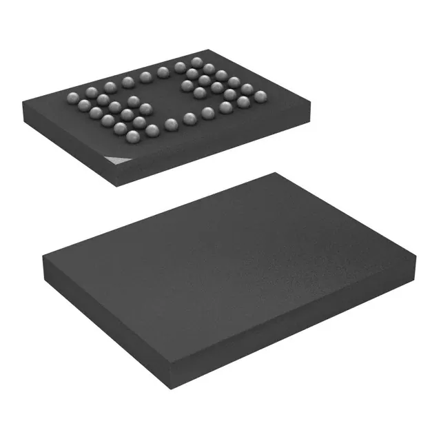
- Part No.:
- CY62138FV30LL-45BVXI
- Manufacturer:
- Cypress Semiconductor Corp
- Category:
- Memory
- Package:
- 36-VFBGA
- Datasheet:
-
 CY62138FV30LL-45BVXI.pdf
- Description:
- IC SRAM 2MBIT PARALLEL 36VFBGA
- Quantity:
- Payment:

- Shipping:

Inventory:492
Please send an inquiry. Send us your inquiry, and we will respond immediately.
Product details
Overview
CY62138FV30LL-45BVXI from Cypress Semiconductor is a 2-Mbit (256 K × 8) CMOS static RAM with 45 ns access time, 2.2–3.6 V supply voltage, and industrial/automotive-A temperature range (–40 °C to +85 °C). It delivers ultra-low standby current (1 µA typical), active current of 1.6 mA at 1 MHz, and automatic power-down on chip deselect-enabling battery-sensitive portable systems such as cellular handsets and handheld medical monitors.
For engineers reviewing the CY62138FV30LL-45BVXI datasheet, CY62138FV30LL-45BVXI pinout, CY62138FV30LL-45BVXI application, or CY62138FV30LL-45BVXI equivalent, key selection criteria include its dual CE architecture for hierarchical memory expansion, VFBGA-36 package compatibility, MoBL® low-power design, and guaranteed 45 ns read/write timing across full voltage and temperature range.
Technical Context
This SRAM implements a synchronous, non-volatile-retentive volatile memory array organized as 256 K words × 8 bits, using complementary metal-oxide-semiconductor (CMOS) process technology optimized for speed-power trade-off. Its dual chip enable (CE1/CE2) logic enables seamless bank selection in multi-SRAM systems without external decoding logic.
The device supports three operational modes: active read (CE1=LOW, CE2=HIGH, OE=LOW, WE=HIGH), active write (CE1=LOW, CE2=HIGH, WE=LOW), and automatic standby (CE1=HIGH or CE2=LOW), with all I/O pins entering high-impedance state during deselect or output disable-ensuring clean bus sharing in 8-bit microcontroller interfaces.
Key Specifications
| Parameter | Value and Actual Design Meaning |
|---|---|
| Memory Size | 256 K × 8 bits = 2 Mbit; supports byte-wide data bus interfacing with 8-bit MCUs and DSPs. |
| Access Time | 45 ns max; guarantees deterministic read latency for real-time firmware execution in industrial controllers. |
| Supply Voltage | 2.2 V to 3.6 V; compatible with Li-ion battery discharge curve and mixed-voltage system rails. |
| Standby Current | 1 µA typical / 5 µA max; enables >1-year battery life in always-on sensor nodes with periodic wake-up. |
| Operating Temp | –40 °C to +85 °C; qualified for under-hood automotive modules and factory-floor PLCs. |
| Package | 36-ball VFBGA (5 mm × 6 mm, 0.5 mm pitch); enables high-density PCB layout in space-constrained IoT edge devices. |
| Input Leakage | ±1 µA max; ensures reliable logic-level recognition even with high-impedance MCU GPIOs. |
Pinout & Package
Package: 36-ball Very Thin Fine-Pitch Ball Grid Array (VFBGA), 5 mm × 6 mm body, 0.5 mm ball pitch, JEDEC MO-220 compliant.
| Pin/Terminal | Circuit Role | Design Meaning |
|---|---|---|
| A0–A17 | Address Inputs | 18-bit address bus supporting full 256 K-word addressing; no internal latching-requires stable address during CE/OE assertion. |
| I/O0–I/O7 | Bidirectional Data Bus | 8-bit tristatable I/O lines; automatically enter high-Z on CE deselect, OE HIGH, or WE LOW-eliminates need for external bus transceivers. |
| CE1, CE2 | Dual Chip Enable | Active-LOW CE1 and active-HIGH CE2 form AND-gated chip select; enables hierarchical memory mapping and reduces decode logic in multi-bank systems. |
| WE | Write Enable | Active-LOW control signal; initiates write when CE1=LOW & CE2=HIGH; timing-critical for meeting 35 ns setup/hold windows. |
| OE | Output Enable | Active-LOW signal enabling read data output; independent of WE-allows read-modify-write sequences without bus contention. |
| VCC, VSS | Power Supply | Single 2.2–3.6 V core supply; no separate I/O voltage rail-simplifies power design in single-rail embedded systems. |
| NC | No Connect | Two unconnected balls (A17, A16 per pin diagram); must be left floating or grounded per PCB layout guidelines-no electrical function. |
Key Features
| Feature | Design Value |
|---|---|
| MoBL® Ultra-Low Power Architecture | 1 µA typical standby current extends battery life in portable medical and telemetry devices beyond 12 months. |
| Dual CE (CE1/CE2) Logic | Enables direct connection to 16-bit address buses (A16/A17) for seamless 512 KB+ memory expansion without glue logic. |
| Automatic Power-Down on Deselect | Eliminates software-controlled sleep mode entry-hardware-triggered transition reduces firmware overhead and improves system responsiveness. |
| 45 ns Guaranteed Timing Across Range | Meets hard real-time deadlines in motor control loops and digital power supply feedback paths without margining. |
| Pb-Free VFBGA Packaging | RoHS-compliant 36-ball VFBGA supports automated reflow assembly and meets IPC/JEDEC standards for thermal cycling reliability. |
Applications
| Portable Cellular Handset Memory | Industrial PLC Data Buffer |
|---|---|
Use Scenario: Storing call logs, SMS messages, and firmware overlay code in GSM/UMTS feature phones with single-cell Li-ion battery. IC Role / Device Role / Timing Role: Byte-accessible SRAM providing non-persistent working memory for baseband processor; 45 ns access synchronizes with 20 MHz Z80-derived MCU clock domain. Use Value: 1 µA standby current enables >18-month shelf life in powered-off state; VFBGA footprint minimizes PCB area in clamshell form factor. | Use Scenario: Caching sensor input buffers and motion-control command queues in DIN-rail mounted programmable logic controllers. IC Role / Device Role / Timing Role: High-reliability volatile memory for deterministic cyclic data exchange between ARM Cortex-M4 CPU and fieldbus interface ASIC. Use Value: –40 °C to +85 °C rating ensures uninterrupted operation in unconditioned factory environments; dual CE supports modular I/O expansion chassis. |
| Automotive Infotainment Display Cache | Handheld Diagnostic Tool RAM |
Use Scenario: Frame buffer storage for 800×480 TFT displays in vehicle head units, buffering UI assets during CAN bus latency spikes. IC Role / Device Role / Timing Role: Low-latency SRAM acting as pixel cache between GPU and display controller; operates at 3.3 V nominal with brown-out immunity down to 2.2 V. Use Value: 45 ns read cycle sustains 60 Hz refresh without frame tearing; automotive-A qualification covers extended temperature cycling in dashboard mounting locations. | Use Scenario: Temporary storage of OBD-II protocol translation tables and live PID streaming buffers in Bluetooth-enabled diagnostic scanners. IC Role / Device Role / Timing Role: Volatile scratchpad memory for ARM Cortex-M0+ host MCU; accessed via 8-bit parallel bus synchronized to internal 24 MHz peripheral clock. Use Value: 2.2–3.6 V operation matches USB-powered 3.3 V LDO output; 5 µA max ISB2 ensures <10 µW quiescent draw during Bluetooth advertising intervals. |
Equivalent & Alternatives
The following parts are listed as comparable options for similar SRAM applications.
| Alternative Part | Technical Difference | Application Difference | Selection Advice |
|---|---|---|---|
| IS62WV2568BLL-45NLI | 45 ns access, same 256 K × 8 organization, but uses 32-pin TSOP-I package and lacks dual CE architecture. | Requires external address decoder for multi-chip expansion; not pin-compatible with VFBGA layout. | Select when board space allows TSOP and legacy footprint reuse is prioritized over power optimization. |
| AS6C4008-45TIN | 45 ns access, 512 K × 8 density, 32-pin SOIC package, 2.7–3.6 V only-no 2.2 V support. | Higher density suits larger buffers but incompatible with low-voltage battery discharge profiles below 2.7 V. | Choose for fixed 3.3 V systems needing >256 KB memory where VFBGA assembly is unavailable. |
Compared with IS62WV2568BLL-45NLI and AS6C4008-45TIN, CY62138FV30LL-45BVXI uniquely combines VFBGA miniaturization, dual CE expandability, 2.2 V operation, and 1 µA standby-making it optimal for next-gen portable and automotive edge devices where size, power, and voltage flexibility are co-constrained.
Availability
CY62138FV30LL-45BVXI is available at Aetrix Electronics and suitable for portable medical monitors, industrial PLC data buffers, and automotive infotainment display caches requiring stable component supply across extended product lifecycles.
Supply support for CY62138FV30LL-45BVXI includes scheduled delivery planning, volume procurement assistance, BOM continuity management, traceable sourcing, and lifecycle availability coordination for OEM customers, industrial embedded developers, connected-device designers, and electronics production programs.
Manufacturer
Cypress Semiconductor (now part of Infineon Technologies) designs high-performance, low-power semiconductor solutions for embedded systems, automotive, and industrial markets.
The CY62138FV30 belongs to the MoBL® (More Battery Life™) SRAM product line, engineered specifically for portable and energy-constrained applications demanding sub-microamp standby current and fast, deterministic access without voltage or temperature derating.
FAQ
What is the minimum VCC required to retain data in CY62138FV30LL-45BVXI?
Data retention is guaranteed down to 1.5 V (VDR), with ICCDR current limited to 4 µA max at that voltage. This allows safe low-power hibernation during brown-out conditions while preserving memory contents-critical for fault logging in automotive ECUs and medical defibrillators.
Does CY62138FV30LL-45BVXI require external pull-up resistors on CE1 or CE2?
No external pull-ups are required: CE1 and CE2 are CMOS-compatible inputs with ±1 µA leakage, designed to interface directly with MCU GPIOs. Internal weak pull-downs are not present; system-level pull-up/pull-down must be implemented per board reset strategy and power-up sequencing requirements.
Can CY62138FV30LL-45BVXI operate reliably at 2.2 V and 85 °C simultaneously?
Yes-the device is fully characterized and guaranteed for 45 ns access time, 5 µA max standby current, and functional operation across the entire industrial/automotive-A range (2.2 V to 3.6 V, –40 °C to +85 °C), including corner-case combinations like 2.2 V/85 °C per AC and DC specifications in Rev. *N datasheet.
How does the dual CE architecture improve memory expansion versus single CE SRAMs?
Dual CE (CE1/CE2) allows direct use of A16 and A17 as chip-select lines-enabling up to four 256 KB banks with zero external logic. This reduces BOM cost, PCB area, and signal routing complexity compared to single-CE parts requiring discrete decoders or CPLDs for >256 KB systems.
CY62138FV30LL-45BVXI Specifications
- Product attributes
- Attribute value
- Manufacturer:
- Cypress Semiconductor Corp
- Series:
- MOBL™
- Package/Case:
- 36-VFBGA
- Packaging:
- Bulk
- Product Status:
- Active
- Programmable:
- Not Verified
- Memory Type:
- Volatile
- Memory Format:
- SRAM
- Technology:
- SRAM - Asynchronous
- Memory Size:
- 2Mbit
- Memory Organization:
- 256K x 8
- Memory Interface:
- Parallel
- Clock Frequency:
- -
- Write Cycle Time - Word, Page:
- 45ns
- Access Time:
- 45 ns
- Voltage - Supply:
- 2.2V ~ 3.6V
- Operating Temperature:
- -40°C ~ 85°C (TA)
- Grade:
- -
- Qualification:
- -
- Mounting Type:
- Surface Mount
- Supplier Device Package:
- 36-VFBGA (6x8)
CY62138FV30LL-45BVXI FAQ
1.How can I place an order for CY62138FV30LL-45BVXI through Aetrix?
Please submit a Request for Quotation (RFQ) for CY62138FV30LL-45BVXI on Aetrix. Our sales agent will provide a competitive quotation and guide you through the order confirmation once you accept the terms.
2.Are the price and stock information for CY62138FV30LL-45BVXI reliable?
The price and inventory of CY62138FV30LL-45BVXI are updated periodically and may fluctuate due to market conditions. Stock and pricing data are typically refreshed every 24 hours. Quotation validity for CY62138FV30LL-45BVXI is usually 5 days.
3.What payment methods are accepted for CY62138FV30LL-45BVXI?
We accept Wire Transfer, PayPal, Credit Card, Western Union, MoneyGram, and Escrow for CY62138FV30LL-45BVXI transactions.
Note: Certain payment methods may incur a processing fee.
4.How is shipping managed for CY62138FV30LL-45BVXI?
CY62138FV30LL-45BVXI orders can be shipped via leading logistics carriers, including DHL, UPS, FedEx, TNT, or Registered Mail.
Once your CY62138FV30LL-45BVXI order is processed, you will receive an email with the shipment details and tracking number.
Note: Tracking information may take up to 24 hours to appear. Express delivery typically takes 3–5 business days.
5.How can I obtain technical support or documentation for CY62138FV30LL-45BVXI?
For technical support, including CY62138FV30LL-45BVXI datasheets, pinout diagrams, or application guidance, please contact our engineering support team. They can provide detailed documentation and assistance for your CY62138FV30LL-45BVXI requirements.
6.How does Aetrix verify that CY62138FV30LL-45BVXI is sourced from the original manufacturer or authorized distributors?
All CY62138FV30LL-45BVXI products on Aetrix are procured from qualified distributors and authorized channels. Our dedicated quality assurance team conducts strict verification, including traceability checks and, if necessary, third-party testing. This ensures that CY62138FV30LL-45BVXI meets industry standards.
7.What is the process for return or replacement of CY62138FV30LL-45BVXI?
All CY62138FV30LL-45BVXI units undergo pre-shipment inspection (PSI). If there is an issue with CY62138FV30LL-45BVXI, returns or replacements are accepted under the following conditions:
1.Quantity discrepancies, incorrect items, or visible external defects (such as breakage or corrosion), acknowledged by Aetrix.
2.The issue is reported within 90 days of delivery.
3.The CY62138FV30LL-45BVXI part is unused and in its original packaging.
Return procedure for CY62138FV30LL-45BVXI:
1.Submit a request within 90 days.
2.Obtain a Return Material Authorization (RMA) from Aetrix.
CY62138FV30LL-45BVXI Tags

-
M24C02-WMN6TP
STMicroelectronics

-
AT24C02C-XHM-T
Microchip Technology

-
AT21CS01-STUM10-T
Microchip Technology

-
AT24C02C-SSHM-T
Microchip Technology

-
24LC01BT-I/OT
Microchip Technology

-
M24C02-FMC6TG
STMicroelectronics
-
AT24CS02-SSHM-T
Microchip Technology

-
93LC46BT-I/OT
Microchip Technology
-
AT24C04C-SSHM-T
Microchip Technology

-
24LC01BT-I/SN
Microchip Technology
-
24AA02UIDT-I/OT
Microchip Technology

-
AT24C08C-STUM-T
Microchip Technology
Tech Hub

Hall effect sensor guide covering working principle, linear and digital sensors, Arduino circuits, current sensing, speed detection, automotive applications, A3144 examples, signal filtering and datash…

Product Change Notification guide for electronic components, covering PCN meaning, PCN vs PDN/EOL, common change types, risk levels, form-fit-function review, engineering validation, BOM control, LTB/L…

A practical guide to blend door actuators, covering HVAC function, symptoms, location, AC and heater issues, reset and calibration, replacement cost, electrical diagnosis, compatibility checks, and rep…

Engineering guide to Raspberry Pi alternatives, covering chip-level differences, Orange Pi, ROCK, Jetson, Banana Pi, NanoPi, Compute Module, Pico, GPIO, camera, HAT compatibility, and replacement risks…

Engineering guide to dynamic load response testing for high-current buck converters, covering load step setup, slew rate, Vcore undershoot, overshoot, recovery time, probe location, output capacitors a…

Engineering guide to output capacitor selection for ASIC Vcore rails, covering bulk capacitors, polymer capacitors, MLCC decoupling, DC bias, ESR, ESL, placement, transient response and substitution ri…

Engineering guide to high-current ASIC Vcore rails, covering 12-phase buck architecture, PMBus control, dynamic load testing, output capacitor networks, smart power stage selection, thermal design and …

Voltage regulator guide covering linear, LDO, 7805, Zener, adjustable, buck, VRM and alternator regulators, with design checks, testing methods, troubleshooting and datasheet-based selection.

Amplifier guide covering voltage, current and power amplification, gain, feedback, amplifier classes, audio and RF applications, op-amp circuits, transimpedance amplifiers, datasheet selection and trou…

Machine vision system guide covering components, inspection workflow, camera and lens selection, FOV, pixel resolution, motion blur, strobe lighting, bandwidth, 2D/3D vision, integration, troubleshooti…


