
 My Inquiry
 My Account


Cypress Semiconductor Corp CY62157ELL-55BVXE
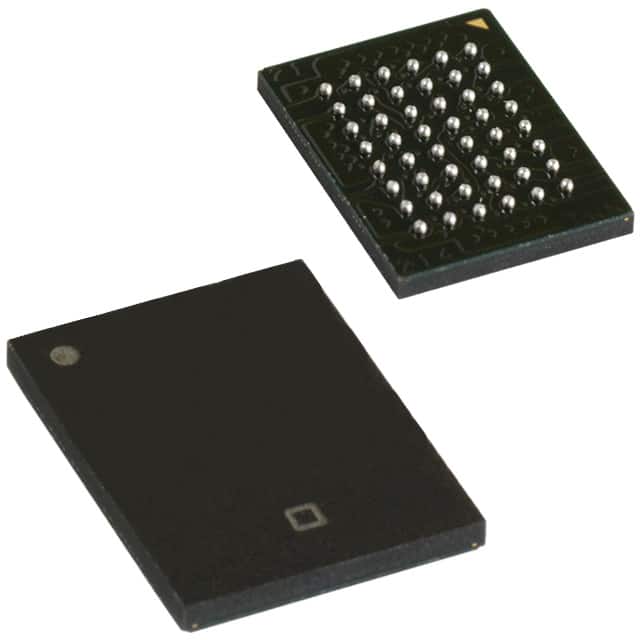
- Part No.:
- CY62157ELL-55BVXE
- Manufacturer:
- Cypress Semiconductor Corp
- Category:
- Memory
- Package:
- 48-VFBGA
- Datasheet:
-
 CY62157ELL-55BVXE.pdf
- Description:
- IC SRAM 8MBIT PARALLEL 48VFBGA
- Quantity:
- Payment:

- Shipping:

Inventory:4,626
Please send an inquiry. Send us your inquiry, and we will respond immediately.
Product details
Overview
CY62157ELL-55BVXE from Cypress Semiconductor is an 8-Mbit (512 K × 16) CMOS static RAM with 45 ns access time, 4.5–5.5 V supply range, and ultra-low standby current (2 µA typical). It supports byte-wide write enable via BHE/ BLE, automatic power-down on deselect, and operates across –40 °C to +85 °C for industrial applications. Used in portable instrumentation and embedded controllers requiring non-volatile data retention during low-power sleep.
For engineers reviewing the CY62157ELL-55BVXE datasheet, CY62157ELL-55BVXE pinout, CY62157ELL-55BVXE application, or CY62157ELL-55BVXE equivalent, key selection criteria include TSOP II package compatibility, TTL-level I/O interface requirements, CE1/CE2 dual-chip-enable logic, and sub-8 µA industrial standby current compliance.
Technical Context
The CY62157ELL-55BVXE implements a 512K × 16 asynchronous SRAM architecture with independent high- and low-byte enables (BHE/ BLE), dual chip enables (CE1 active-low, CE2 active-high), and automatic power-down triggered by CE or byte-enable deassertion. Its TTL-compatible input thresholds (VIH ≥ 2.2 V, VIL ≤ 0.8 V) require external level-shifting when interfacing with pure CMOS processors.
Timing is defined by overlapping control signals: read access requires CE1 LOW + CE2 HIGH + OE LOW + WE HIGH; write requires CE1 LOW + CE2 HIGH + WE LOW with BHE or BLE LOW. Data retention is guaranteed down to 2 V VCC, with tCDR = 0 ns and ICCDR ≤ 8 µA at VCC = 2 V.
Key Specifications
| Parameter | Value and Actual Design Meaning |
|---|---|
| Memory Size | 8 Mbit (512 K × 16) - provides 1 MB of fast, non-refreshing data storage for real-time buffering. |
| Access Time | 45 ns - ensures compatibility with 22 MHz bus systems without wait states. |
| VCC Range | 4.5 V–5.5 V - supports legacy 5 V logic rails and tolerates ±10% supply variation. |
| Standby Current | 2 µA typical / 8 µA max (Industrial) - enables multi-year battery operation in always-on sensor nodes. |
| Operating Temp | –40 °C to +85 °C - qualified for industrial control cabinets and automotive under-hood ECUs. |
| I/O Interface | TTL-compatible inputs - eliminates need for external level shifters when connected to 5 V microcontrollers. |
| Data Retention VCC | 2 V minimum - maintains memory contents during brown-out conditions without backup capacitor. |
Pinout & Package
Package: 44-pin TSOP II (Thin Small Outline Package, Type II), 400 mil width, lead-free finish.
| Pin/Terminal | Circuit Role | Design Meaning |
|---|---|---|
| A0–A18 | Address Inputs | 19-bit address bus supporting full 512K-word addressing; no internal multiplexing. |
| I/O0–I/O7 | Data Bus (Low Byte) | Bi-directional 8-bit data path enabled only when BLE = LOW and device is selected. |
| I/O8–I/O15 | Data Bus (High Byte) | Bi-directional 8-bit data path enabled only when BHE = LOW and device is selected. |
| CE1 | Chip Enable 1 | Active-LOW primary chip select; device enters standby if HIGH while CE2 is HIGH. |
| CE2 | Chip Enable 2 | Active-HIGH secondary chip select; must be HIGH for normal operation; complements CE1 logic. |
| OE | Output Enable | Active-LOW control for output drivers; places I/O pins in high-Z when HIGH during read cycles. |
| WE | Write Enable | Active-LOW signal initiating write; latches data on rising edge when CE1/CE2 active. |
| BLE | Byte Low Enable | Active-LOW control enabling writes/reads to I/O0–I/O7 only; supports 8-bit bus interfacing. |
| BHE | Byte High Enable | Active-LOW control enabling writes/reads to I/O8–I/O15 only; enables 16-bit or split-bus operation. |
| VCC | Power Supply | 4.5–5.5 V core voltage; two dedicated VCC pins reduce IR drop in high-speed operation. |
| VSS | Ground | Two ground pins provide low-inductance return paths for I/O and core logic switching currents. |
Key Features
| Feature | Design Value |
|---|---|
| Ultra-low standby power | 2 µA typical ISB2 enables >10-year battery life in metering and remote telemetry devices. |
| Dual chip enable logic | CE1 (active-LOW) + CE2 (active-HIGH) allows hierarchical memory mapping and seamless expansion beyond 1 MB. |
| Independent byte enables | BHE/ BLE support mixed 8-bit/16-bit peripheral interfacing without external glue logic or data masking. |
| Automatic power-down | Enters low-power mode within 0 ns (tCDR = 0) when CE1 HIGH or CE2 LOW or both BHE/ BLE HIGH - no software overhead. |
| TTL-compatible I/O | VIH ≥ 2.2 V / VIL ≤ 0.8 V matches legacy 5 V microcontrollers (e.g., 8051, PIC18F) without level shifters. |
Applications
| Portable Medical Monitor | Industrial PLC I/O Module |
|---|---|
|
Use Scenario: Real-time ECG waveform buffering during battery-powered operation with periodic flash offload. IC Role / Device Role / Timing Role: Asynchronous SRAM buffer holding 16-bit sample streams; accessed at 10 kHz with burst reads every 500 ms. Use Value: 2 µA standby current extends single-AA battery life to >3 years; 45 ns access avoids CPU wait states during DMA transfers. |
Use Scenario: Local register storage for analog input/output channel configuration and calibration data in DIN-rail mounted controllers. IC Role / Device Role / Timing Role: Non-volatile shadow RAM storing 512×16-bit channel maps; updated only during firmware initialization or field recalibration. Use Value: Dual CE logic enables isolation from main backplane bus during hot-swap events; 8 µA max ISB2 ensures thermal stability in enclosed enclosures. |
| Automotive Body Control Unit | Smart Energy Meter |
|
Use Scenario: Storing door lock status, window position, and lighting profiles across ignition cycles in Class A vehicle modules. IC Role / Device Role / Timing Role: Power-fail resilient data latch; retains values during 2 V brown-out events lasting up to 100 ms. Use Value: Guaranteed data retention at VCC = 2 V eliminates need for supercapacitor backup; –40 °C to +125 °C automotive grade ensures reliability under hood. |
Use Scenario: Holding tamper-event logs, tariff schedules, and communication stack buffers in ANSI C12.22-compliant meters. IC Role / Device Role / Timing Role: High-reliability scratchpad memory accessed by 8-bit MCU over parallel bus; survives 100,000+ write cycles. Use Value: TTL-level compatibility eliminates level-shifter BOM cost; 44-pin TSOP II footprint simplifies rework and conforms to IPC-7351B standards. |
Equivalent & Alternatives
The following parts are listed as comparable options for similar SRAM applications.
| Alternative Part | Technical Difference | Application Difference | Selection Advice |
|---|---|---|---|
| IS62WV51216BLL-45NLI | 45 ns access, 3.3 V only (2.7–3.6 V), CMOS I/O levels, 48-ball VFBGA only | Requires level-shifting for 5 V systems; better suited for new 3.3 V designs with space constraints | Select if migrating to 3.3 V architecture and board layout supports VFBGA reflow. |
| AS6C4008-55TIN | 55 ns access, 4.5–5.5 V, TTL I/O, 44-pin TSOP II, 8 µA max ISB | Slower timing but identical package and interface; higher max standby current (8 µA vs 8 µA same spec) | Select for cost-sensitive industrial designs where 55 ns timing is acceptable and second-source assurance is required. |
Compared with IS62WV51216BLL-45NLI and AS6C4008-55TIN, the CY62157ELL-55BVXE uniquely combines 45 ns speed, 5 V TTL compatibility, and 44-pin TSOP II packaging - making it optimal for legacy 5 V controller upgrades without PCB redesign.
Availability
CY62157ELL-55BVXE is available at Aetrix Electronics and suitable for portable medical monitors, industrial PLC I/O modules, and automotive body control units requiring stable component supply across extended product lifecycles.
Supply support for CY62157ELL-55BVXE includes scheduled delivery planning, volume procurement assistance, BOM continuity management, traceable sourcing, and lifecycle availability coordination for OEM customers, industrial embedded developers, connected-device designers, and electronics production programs.
Manufacturer
Cypress Semiconductor (now part of Infineon Technologies) designs high-reliability memory and programmable solutions for industrial, automotive, and IoT applications.
The CY62157E MoBL® SRAM product line targets battery-constrained portable electronics, emphasizing ultra-low standby current, TTL compatibility, and robust data retention - not general-purpose computing memory.
FAQ
Is CY62157ELL-55BVXE compatible with 3.3 V microcontrollers?
No. The CY62157ELL-55BVXE requires 4.5–5.5 V VCC and features TTL-level inputs (VIH ≥ 2.2 V, VIL ≤ 0.8 V), not 3.3 V CMOS thresholds. Interfacing with 3.3 V MCUs requires bidirectional level shifters such as TXB0108 or discrete MOSFET translators to avoid logic misreads and excessive input leakage.
What happens if both CE1 and CE2 are asserted simultaneously?
When CE1 is LOW and CE2 is HIGH, the device operates normally. If CE1 is LOW and CE2 is LOW, the device enters high-impedance standby regardless of OE or WE state. If CE1 is HIGH and CE2 is HIGH, the device remains deselected and draws ISB2 current. CE1 HIGH + CE2 LOW is an invalid state per datasheet truth table and must be avoided.
Can BHE and BLE be tied permanently LOW for full 16-bit operation?
Yes. Tying both BHE and BLE LOW enables full 16-bit data transfers on I/O0–I/O15. This configuration is valid and commonly used in 16-bit bus systems. However, doing so forfeits byte-select capability and increases active current slightly due to double the I/O capacitance being driven.
Does CY62157ELL-55BVXE support battery backup mode?
It supports data retention down to 2 V VCC with ICCDR ≤ 8 µA, but lacks built-in battery-switching circuitry. External diode-OR or ideal diode controllers (e.g., LTC4412) must be added to switch between main supply and backup battery. The device itself does not monitor VCC or initiate switchover.
CY62157ELL-55BVXE Specifications
- Product attributes
- Attribute value
- Manufacturer:
- Cypress Semiconductor Corp
- Series:
- MOBL™
- Package/Case:
- 48-VFBGA
- Packaging:
- Bulk
- Product Status:
- Active
- Programmable:
- Not Verified
- Memory Type:
- Volatile
- Memory Format:
- SRAM
- Technology:
- SRAM - Asynchronous
- Memory Size:
- 8Mbit
- Memory Organization:
- 512K x 16
- Memory Interface:
- Parallel
- Clock Frequency:
- -
- Write Cycle Time - Word, Page:
- 55ns
- Access Time:
- 55 ns
- Voltage - Supply:
- 4.5V ~ 5.5V
- Operating Temperature:
- -40°C ~ 125°C (TA)
- Grade:
- -
- Qualification:
- -
- Mounting Type:
- Surface Mount
- Supplier Device Package:
- 48-VFBGA (6x8)
CY62157ELL-55BVXE FAQ
1.How can I place an order for CY62157ELL-55BVXE through Aetrix?
Please submit a Request for Quotation (RFQ) for CY62157ELL-55BVXE on Aetrix. Our sales agent will provide a competitive quotation and guide you through the order confirmation once you accept the terms.
2.Are the price and stock information for CY62157ELL-55BVXE reliable?
The price and inventory of CY62157ELL-55BVXE are updated periodically and may fluctuate due to market conditions. Stock and pricing data are typically refreshed every 24 hours. Quotation validity for CY62157ELL-55BVXE is usually 5 days.
3.What payment methods are accepted for CY62157ELL-55BVXE?
We accept Wire Transfer, PayPal, Credit Card, Western Union, MoneyGram, and Escrow for CY62157ELL-55BVXE transactions.
Note: Certain payment methods may incur a processing fee.
4.How is shipping managed for CY62157ELL-55BVXE?
CY62157ELL-55BVXE orders can be shipped via leading logistics carriers, including DHL, UPS, FedEx, TNT, or Registered Mail.
Once your CY62157ELL-55BVXE order is processed, you will receive an email with the shipment details and tracking number.
Note: Tracking information may take up to 24 hours to appear. Express delivery typically takes 3–5 business days.
5.How can I obtain technical support or documentation for CY62157ELL-55BVXE?
For technical support, including CY62157ELL-55BVXE datasheets, pinout diagrams, or application guidance, please contact our engineering support team. They can provide detailed documentation and assistance for your CY62157ELL-55BVXE requirements.
6.How does Aetrix verify that CY62157ELL-55BVXE is sourced from the original manufacturer or authorized distributors?
All CY62157ELL-55BVXE products on Aetrix are procured from qualified distributors and authorized channels. Our dedicated quality assurance team conducts strict verification, including traceability checks and, if necessary, third-party testing. This ensures that CY62157ELL-55BVXE meets industry standards.
7.What is the process for return or replacement of CY62157ELL-55BVXE?
All CY62157ELL-55BVXE units undergo pre-shipment inspection (PSI). If there is an issue with CY62157ELL-55BVXE, returns or replacements are accepted under the following conditions:
1.Quantity discrepancies, incorrect items, or visible external defects (such as breakage or corrosion), acknowledged by Aetrix.
2.The issue is reported within 90 days of delivery.
3.The CY62157ELL-55BVXE part is unused and in its original packaging.
Return procedure for CY62157ELL-55BVXE:
1.Submit a request within 90 days.
2.Obtain a Return Material Authorization (RMA) from Aetrix.
CY62157ELL-55BVXE Tags

-
M24C02-WMN6TP
STMicroelectronics

-
AT24C02C-XHM-T
Microchip Technology

-
AT21CS01-STUM10-T
Microchip Technology

-
AT24C02C-SSHM-T
Microchip Technology

-
24LC01BT-I/OT
Microchip Technology

-
M24C02-FMC6TG
STMicroelectronics
-
AT24CS02-SSHM-T
Microchip Technology

-
93LC46BT-I/OT
Microchip Technology
-
AT24C04C-SSHM-T
Microchip Technology

-
24LC01BT-I/SN
Microchip Technology
-
24AA02UIDT-I/OT
Microchip Technology

-
AT24C08C-STUM-T
Microchip Technology
Tech Hub

Hall effect sensor guide covering working principle, linear and digital sensors, Arduino circuits, current sensing, speed detection, automotive applications, A3144 examples, signal filtering and datash…

Product Change Notification guide for electronic components, covering PCN meaning, PCN vs PDN/EOL, common change types, risk levels, form-fit-function review, engineering validation, BOM control, LTB/L…

A practical guide to blend door actuators, covering HVAC function, symptoms, location, AC and heater issues, reset and calibration, replacement cost, electrical diagnosis, compatibility checks, and rep…

Engineering guide to Raspberry Pi alternatives, covering chip-level differences, Orange Pi, ROCK, Jetson, Banana Pi, NanoPi, Compute Module, Pico, GPIO, camera, HAT compatibility, and replacement risks…

Engineering guide to dynamic load response testing for high-current buck converters, covering load step setup, slew rate, Vcore undershoot, overshoot, recovery time, probe location, output capacitors a…

Engineering guide to output capacitor selection for ASIC Vcore rails, covering bulk capacitors, polymer capacitors, MLCC decoupling, DC bias, ESR, ESL, placement, transient response and substitution ri…

Engineering guide to high-current ASIC Vcore rails, covering 12-phase buck architecture, PMBus control, dynamic load testing, output capacitor networks, smart power stage selection, thermal design and …

Voltage regulator guide covering linear, LDO, 7805, Zener, adjustable, buck, VRM and alternator regulators, with design checks, testing methods, troubleshooting and datasheet-based selection.

Amplifier guide covering voltage, current and power amplification, gain, feedback, amplifier classes, audio and RF applications, op-amp circuits, transimpedance amplifiers, datasheet selection and trou…

Machine vision system guide covering components, inspection workflow, camera and lens selection, FOV, pixel resolution, motion blur, strobe lighting, bandwidth, 2D/3D vision, integration, troubleshooti…


