
 My Inquiry
 My Account


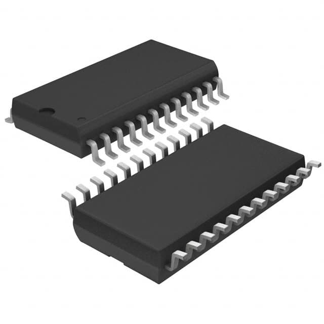
Infineon Technologies CY7B952-SXC
- Part No.:
- CY7B952-SXC
- Manufacturer:
- Infineon Technologies
- Category:
- Drivers, Receivers, Transceivers
- Package:
- 24-SOIC (0.295", 7.50mm Width)
- Datasheet:
-
 CY7B952-SXC.pdf
- Description:
- IC TRANSCEIVER FULL 24SOIC
- Quantity:
- Payment:

- Shipping:

Inventory:4,449
Please send an inquiry. Send us your inquiry, and we will respond immediately.
Product details
Overview
CY7B952-SXC from Cypress Semiconductor is a SONET/SDH serial transceiver IC supporting OC-3 (155.52 MHz) and OC-1 (51.84 MHz) data rates with integrated clock/data recovery (CDR), 8× frequency multiplication, differential ECL 100K I/O, ±1% frequency agility, and compliance with Bellcore GR-253-Core and ITU-T G.958. It serves as the physical layer interface in telecom line cards and ATM edge equipment.
For engineers reviewing the CY7B952-SXC datasheet, CY7B952-SXC pinout, CY7B952-SXC application, or CY7B952-SXC equivalent, key selection criteria include jitter generation (<0.01 UI), REFCLK×8 multiplication accuracy, LFI/CD control logic, loop-back test capability, and SOIC-24 compatibility with fiber-optic and copper media interfaces.
Technical Context
The CY7B952-SXC integrates two independent PLLs: a receive CDR PLL that recovers RCLK± and RSER± from RIN± at 51.84 or 155.52 MHz, and a transmit PLL that multiplies REFCLK± by 8 to generate TCLK±. Both PLLs are synchronized to the same REFCLK source and share MODE-driven frequency selection.
Its three-level MODE pin configures operation for STS-1 (51.84 MHz), STS-3 (155.52 MHz), or factory test mode; FC± pins connect external 301kΩ ±1% resistor and 1µF ±10% capacitor for PLL loop damping; LFI output reflects real-time lock status via CD input, transition detection, and OOL monitoring.
Key Specifications
| Parameter | Value and Actual Design Meaning |
|---|---|
| Data Rate | 51.84 MHz (STS-1) or 155.52 MHz (STS-3); selectable via MODE pin - enables dual-rate deployment without hardware change. |
| Jitter Generation | <0.01 UI - meets Bellcore GR-253-Core requirement for OC-3 line interface stability. |
| REFCLK Multiplication | ×8 fixed ratio - allows low-cost 6.48 MHz or 19.44 MHz crystal sources to drive full-rate transmission. |
| I/O Standard | ECL 100K (VCC-referenced) - supports direct connection to optical drivers and coaxial/twisted-pair media without level-shifting. |
| Power Supply | +5 V single supply - simplifies power design; operating current <70 mA reduces thermal load in dense line cards. |
| Frequency Agility | ±1% - accommodates crystal tolerance and temperature drift while maintaining lock under GR-253-compliant jitter transfer. |
| Input Sensitivity | 50 mV differential minimum on RIN±/TSER± - eliminates need for external pre-amplifiers with low-swing PECL sources. |
Pinout & Package
Package: 24-pin SOIC (Small Outline Integrated Circuit), surface-mount, JEDEC MS-013AC compliant.
| Pin/Terminal | Circuit Role | Design Meaning |
|---|---|---|
| RIN± | Differential Receive Input | Direct interface to optical module or copper line receiver; no external buffering required; wide common-mode range (2.5 V). |
| RSER±, RCLK± | Differential Recovered Data/Clock Outputs | Aligned ECL 100K outputs synchronized to recovered bit stream; timing compatible with downstream framer or mapper ICs. |
| TSER± | Differential Transmit Input | Accepts upstream serial data; rebuffered to TOUT±; supports loop-back testing when MODE/LOOP configured. |
| TOUT±, TCLK± | Differential Transmit Output / Clock | Drive low-impedance media directly; TCLK± provides bit-rate clock for serializer or multiplexer timing. |
| REFCLK± | Differential/TTL Reference Clock Input | Configurable as PECL or TTL input; multiplied ×8 internally to set center frequency for both PLLs. |
| CD, LFI, LOOP, MODE | Control Logic Inputs/Outputs | Enable carrier detection, link fault reporting, internal loop-back, and dual-rate selection - all TTL/ECL compatible. |
Key Features
| Feature | Design Value |
|---|---|
| Integrated CDR + Frequency Multiplier | Single-chip solution replaces discrete PLL + buffer + mux; eliminates inter-stage skew and board-area overhead. |
| Three-Level MODE Selection | Hardware-selectable STS-1/STS-3/test modes via single pin - avoids firmware configuration and enables field rate reconfiguration. |
| Link Fault Indicator (LFI) | Combines CD status, transition density, and PLL lock state into one TTL output - simplifies LOS/LOF monitoring in NMS systems. |
| Power-Down Control | Individual shutdown of receive/transmit PLLs by floating or tying RSER±/RCLK± or TCLK± to VCC - reduces idle power and crosstalk. |
| FC± Loop Filter Interface | External RC network (301kΩ + 1µF) sets PLL bandwidth and damping - enables tuning for specific jitter transfer requirements per GR-253. |
Applications
| OC-3 Line Interface Card | ATM Edge Concentrator |
|---|---|
Use Scenario: Telecom central office line card interfacing with OC-3 fiber links carrying DS3 or ATM cells. IC Role / Device Role / Timing Role: Physical layer transceiver performing clock/data recovery, jitter filtering, and transmit re-timing at 155.52 MHz. Use Value: Meets Bellcore GR-253 jitter specs without external jitter cleaners; reduces BOM count by integrating CDR and ×8 PLL. |
Use Scenario: Aggregation node converting multiple DS1/DS3 streams into ATM cells for backbone transport. IC Role / Device Role / Timing Role: Serial interface bridging framer output to optical PHY; provides stable TCLK± for cell segmentation timing. Use Value: REFCLK×8 multiplication enables use of low-cost 19.44 MHz crystals instead of 155.52 MHz oscillators - cuts timing subsystem cost by >40%. |
| SONET Add-Drop Multiplexer (ADM) | Test & Measurement Equipment |
Use Scenario: Field-deployable ADM supporting drop-and-insert of VT1.5/VT2 tributaries over OC-3 line. IC Role / Device Role / Timing Role: Dual-role transceiver handling both line-side CDR and path-side transmit buffering with loop-back support. Use Value: LOOP and MODE pins enable in-system verification of receive lock and transmit integrity without external pattern generators. |
Use Scenario: Bit-error-rate tester (BERT) front-end module validating OC-3 signal integrity and jitter compliance. IC Role / Device Role / Timing Role: Reference CDR for golden clock recovery; LFI and CD signals feed automated pass/fail decision logic. Use Value: Built-in jitter generation <0.01 UI and jitter tolerance per G.958 allow direct comparison against compliance masks in real time. |
Equivalent & Alternatives
The following parts are listed as comparable options for similar SONET/SDH transceiver applications.
| Alternative Part | Technical Difference | Application Difference | Selection Advice |
|---|---|---|---|
| PMC-Sierra PM5343STXC | Same 24-pin SOIC package; requires external loop filter components; no integrated LFI logic - relies on host processor for fault detection. | Used in legacy PMC-based SONET framers; lacks native CD/LFI integration - increases software overhead for LOS handling. | Select when migrating from existing PMC designs or when tighter jitter transfer tuning is needed via discrete filter. |
| Exar XR22061ILF | Supports OC-3 only (no STS-1 mode); uses LVPECL I/O (3.3 V) vs. CY7B952's ECL 100K (5 V); lower power (45 mA) but no MODE-driven dual-rate flexibility. | Targeted at newer 3.3 V systems with space-constrained layouts; incompatible with legacy 5 V PECL backplanes. | Select for new 3.3 V designs prioritizing power efficiency over multi-rate field reconfiguration. |
Compared with PM5343STXC and XR22061ILF, the CY7B952-SXC uniquely combines dual-rate hardware selection, integrated LFI/CD logic, and 5 V ECL 100K drive strength - making it optimal for retrofitting legacy OC-1/OC-3 line cards requiring minimal system-level changes.
Availability
CY7B952-SXC is available at Aetrix Electronics and suitable for OC-3 line interface cards, ATM edge concentrators, and SONET add-drop multiplexers requiring stable component supply across extended product lifecycles.
Supply support for CY7B952-SXC includes scheduled delivery planning, volume procurement assistance, BOM continuity management, traceable sourcing, and lifecycle availability coordination for OEM customers, industrial embedded developers, connected-device designers, and electronics production programs.
Manufacturer
Cypress Semiconductor (now part of Infineon Technologies) is a U.S.-based semiconductor company specializing in programmable systems-on-chip, memory, and interface solutions for communications and industrial markets.
The CY7B952 belongs to Cypress's SST™ SONET/SDH Transceiver product line, designed specifically for carrier-grade optical transport equipment requiring deterministic jitter performance and multi-standard interoperability.
FAQ
What reference clock frequencies are supported for OC-3 and OC-1 operation?
The CY7B952-SXC requires a 19.44 MHz ±1% REFCLK for OC-3 (155.52 MHz) operation and a 6.48 MHz ±1% REFCLK for OC-1 (51.84 MHz) operation. Both are multiplied internally by 8. The MODE pin selects between these two modes, and REFCLK must be applied differentially (REFCLK±) or as a single-ended TTL signal on either pin.
How does the Link Fault Indicator (LFI) determine fault conditions?
LFI asserts LOW when any of three conditions occur: Carrier Detect (CD) is pulled low, the internal transition detector identifies insufficient data transitions on RIN±, or the Out-of-Lock (OOL) circuit detects frequency deviation beyond ±1000 ppm. When CD is TTL LOW, LFI responds only to OOL - enabling selective fault masking in hybrid systems.
Can the CY7B952-SXC operate with a single-ended TTL clock source?
Yes. When either REFCLK+ or REFCLK– is held at TTL LOW, the other pin becomes a single-ended TTL input. This allows direct connection to low-cost 6.48 MHz or 19.44 MHz TTL crystal oscillators without level-shifting circuitry - verified in Section 5 of the Rev. *E datasheet.
What is the purpose of the FC± pins and what external components are required?
FC± connects to an external RC network that sets the loop bandwidth and damping factor of the receive CDR PLL. A 301 kΩ ±1% resistor and 1 µF ±10% non-polar capacitor must be placed in parallel and mounted as close as possible to the FC± pins on the PCB to meet Bellcore jitter transfer specifications.
CY7B952-SXC Specifications
- Product attributes
- Attribute value
- Manufacturer:
- Infineon Technologies
- Series:
- -
- Package/Case:
- 24-SOIC (0.295", 7.50mm Width)
- Packaging:
- Tube
- Product Status:
- Obsolete
- Type:
- Transceiver
- Protocol:
- -
- Number of Drivers/Receivers:
- -
- Duplex:
- Full
- Receiver Hysteresis:
- -
- Data Rate:
- -
- Voltage - Supply:
- 4.5V ~ 5.5V
- Operating Temperature:
- 0°C ~ 70°C
- Grade:
- -
- Qualification:
- -
- Mounting Type:
- Surface Mount
- Supplier Device Package:
- 24-SOIC
CY7B952-SXC FAQ
1.How can I place an order for CY7B952-SXC through Aetrix?
Please submit a Request for Quotation (RFQ) for CY7B952-SXC on Aetrix. Our sales agent will provide a competitive quotation and guide you through the order confirmation once you accept the terms.
2.Are the price and stock information for CY7B952-SXC reliable?
The price and inventory of CY7B952-SXC are updated periodically and may fluctuate due to market conditions. Stock and pricing data are typically refreshed every 24 hours. Quotation validity for CY7B952-SXC is usually 5 days.
3.What payment methods are accepted for CY7B952-SXC?
We accept Wire Transfer, PayPal, Credit Card, Western Union, MoneyGram, and Escrow for CY7B952-SXC transactions.
Note: Certain payment methods may incur a processing fee.
4.How is shipping managed for CY7B952-SXC?
CY7B952-SXC orders can be shipped via leading logistics carriers, including DHL, UPS, FedEx, TNT, or Registered Mail.
Once your CY7B952-SXC order is processed, you will receive an email with the shipment details and tracking number.
Note: Tracking information may take up to 24 hours to appear. Express delivery typically takes 3–5 business days.
5.How can I obtain technical support or documentation for CY7B952-SXC?
For technical support, including CY7B952-SXC datasheets, pinout diagrams, or application guidance, please contact our engineering support team. They can provide detailed documentation and assistance for your CY7B952-SXC requirements.
6.How does Aetrix verify that CY7B952-SXC is sourced from the original manufacturer or authorized distributors?
All CY7B952-SXC products on Aetrix are procured from qualified distributors and authorized channels. Our dedicated quality assurance team conducts strict verification, including traceability checks and, if necessary, third-party testing. This ensures that CY7B952-SXC meets industry standards.
7.What is the process for return or replacement of CY7B952-SXC?
All CY7B952-SXC units undergo pre-shipment inspection (PSI). If there is an issue with CY7B952-SXC, returns or replacements are accepted under the following conditions:
1.Quantity discrepancies, incorrect items, or visible external defects (such as breakage or corrosion), acknowledged by Aetrix.
2.The issue is reported within 90 days of delivery.
3.The CY7B952-SXC part is unused and in its original packaging.
Return procedure for CY7B952-SXC:
1.Submit a request within 90 days.
2.Obtain a Return Material Authorization (RMA) from Aetrix.
CY7B952-SXC Tags

-
ATA6561-GAQW-N
Microchip Technology
-
ATA6561-GBQW-N
Microchip Technology

-
AM26LS32ACDR
Texas Instruments

-
SP485CN-L/TR
MaxLinear, Inc.
-
SP485EN-L/TR
MaxLinear, Inc.
-
SP485EEN-L/TR
MaxLinear, Inc.
-
SP485ECN-L/TR
MaxLinear, Inc.
-
THVD1400DR
Texas Instruments
-
AM26C31IDR
Texas Instruments

-
TLIN1021ADRQ1
Texas Instruments
-
MAX232IDR
Texas Instruments
-
AM26C32IDR
Texas Instruments
Tech Hub

Guide to electronic component obsolescence covering EOL risk, PCN/PDN notices, last-time buy planning, replacement options, form-fit-function validation, counterfeit risk and BOM lifecycle management.

18650 battery guide covering lithium-ion cell basics, 3.6V/3.7V voltage, 4.2V charging, mAh and Wh capacity, protected cells, chargers, BMS, series-parallel packs, holders, welding and sourcing checks.…

Hall effect sensor guide covering working principle, linear and digital sensors, Arduino circuits, current sensing, speed detection, automotive applications, A3144 examples, signal filtering and datash…

Product Change Notification guide for electronic components, covering PCN meaning, PCN vs PDN/EOL, common change types, risk levels, form-fit-function review, engineering validation, BOM control, LTB/L…

A practical guide to blend door actuators, covering HVAC function, symptoms, location, AC and heater issues, reset and calibration, replacement cost, electrical diagnosis, compatibility checks, and rep…

Engineering guide to Raspberry Pi alternatives, covering chip-level differences, Orange Pi, ROCK, Jetson, Banana Pi, NanoPi, Compute Module, Pico, GPIO, camera, HAT compatibility, and replacement risks…

Engineering guide to dynamic load response testing for high-current buck converters, covering load step setup, slew rate, Vcore undershoot, overshoot, recovery time, probe location, output capacitors a…

Engineering guide to output capacitor selection for ASIC Vcore rails, covering bulk capacitors, polymer capacitors, MLCC decoupling, DC bias, ESR, ESL, placement, transient response and substitution ri…

Engineering guide to high-current ASIC Vcore rails, covering 12-phase buck architecture, PMBus control, dynamic load testing, output capacitor networks, smart power stage selection, thermal design and …

Voltage regulator guide covering linear, LDO, 7805, Zener, adjustable, buck, VRM and alternator regulators, with design checks, testing methods, troubleshooting and datasheet-based selection.


