
 My Inquiry
 My Account


Cypress Semiconductor Corp CY7C1011G30-10ZSXA
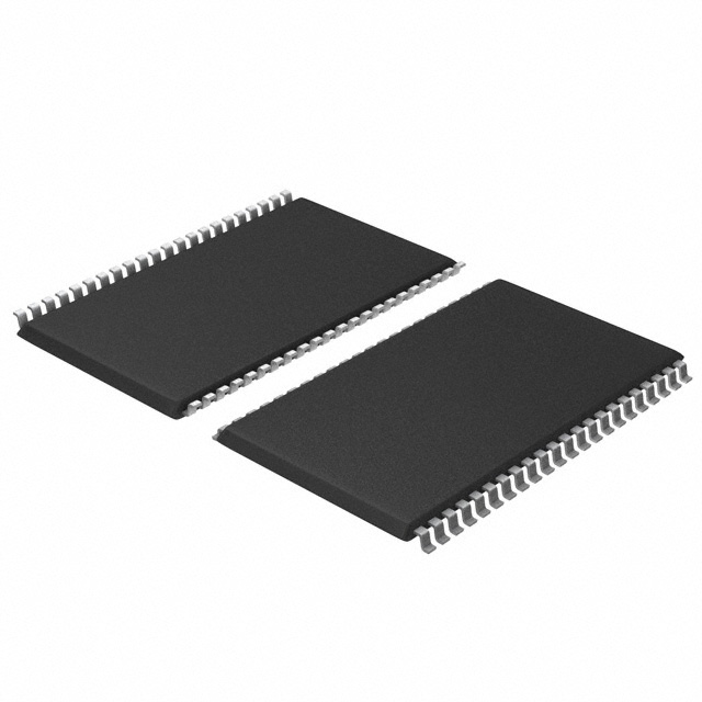
- Part No.:
- CY7C1011G30-10ZSXA
- Manufacturer:
- Cypress Semiconductor Corp
- Category:
- Memory
- Package:
- 44-TSOP (0.400", 10.16mm Width)
- Datasheet:
-
 CY7C1011G30-10ZSXA.pdf
- Description:
- IC SRAM 2MBIT PARALLEL 44TSOP II
- Quantity:
- Payment:

- Shipping:

Inventory:437
Please send an inquiry. Send us your inquiry, and we will respond immediately.
Product details
Overview
CY7C1011G30-10ZSXA from Infineon Technologies (formerly Cypress) is an automotive-grade 2-Mbit (128K × 16-bit) CMOS static RAM with embedded single-bit error-correcting code (ECC), operating at 10 ns access time over –40 °C to +125 °C, supporting 2.2 V–3.6 V supply and TTL-compatible I/O for safety-critical memory subsystems in engine control units.
For engineers reviewing the CY7C1011G30-10ZSXA datasheet, CY7C1011G30-10ZSXA pinout, CY7C1011G30-10ZSXA application, or CY7C1011G30-10ZSXA equivalent, key selection factors include AEC-Q100 qualification, ECC implementation without automatic write-back, dual-byte enable (BHE/ BLE) control, and VFBGA48/TSOP II package compatibility in automotive-E temperature grade.
Technical Context
The CY7C1011G30-10ZSXA implements a synchronous SRAM architecture with dedicated ECC encoder/decoder logic adjacent to the 128K × 16-bit memory array, detecting and correcting single-bit errors on read paths only - no error injection or write-back capability. It uses a single Chip Enable (CE) with active-low assertion and supports byte-level writes via independent BHE (I/O8–I/O15) and BLE (I/O0–I/O7) controls.
Timing is governed by strict AC parameters including tAA = 10 ns (max), tACE = 10 ns (max), and tDOE = 4.5 ns (max), with all I/Os entering high-impedance state when CE is HIGH or OE/BHE/BLE are deasserted. Data retention operates down to 1.0 V at ambient temperatures up to 125 °C, with ISB2 = 6 mA typical standby current under CMOS input conditions.
Key Specifications
| Parameter | Value and Actual Design Meaning |
|---|---|
| Memory size | 2 Mbit (128K words × 16-bit); provides full-word parallel access for microcontroller bus interfacing without external multiplexing. |
| Access time (tAA) | 10 ns max at VCC = 2.2–3.6 V, –40 °C to +125 °C; enables direct interface with 100 MHz bus clocks in real-time ECUs. |
| ECC capability | Single-bit error correction per 16-bit word; implemented in hardware with no software overhead, but no automatic write-back on correction. |
| Supply voltage | 2.2 V–3.6 V operation; compatible with automotive 3.3 V domains and tolerant of battery transients down to 2.2 V. |
| Standby current (ISB2) | 6 mA typical at VCC = 3.6 V, CMOS inputs; supports low-power sleep modes in always-on vehicle modules. |
| Temperature grade | Automotive-E (–40 °C to +125 °C); qualified per AEC-Q100 Grade 0, suitable for under-hood ECU deployment. |
| Data retention voltage | 1.0 V minimum; maintains stored data during brown-out or stop-mode operation without backup power. |
Pinout & Package
Package: 48-ball Very Thin Fine-Pitch Ball Grid Array (VFBGA), 6 mm × 8 mm, 0.5 mm pitch, RoHS-compliant, moisture sensitivity level 3.
| Pin/Terminal | Circuit Role | Design Meaning |
|---|---|---|
| A0–A16 | Address inputs | 17-bit address bus supporting full 128K-word addressing; internally decoded without external latch requirement. |
| I/O0–I/O15 | Bidirectional data lines | 16-bit parallel data path; high-impedance when CE HIGH or OE/BHE/BLE inactive, enabling bus sharing. |
| CE | Chip Enable | Active-low global enable; device enters low-power ISB2 mode when HIGH, eliminating need for external power gating. |
| OE | Output Enable | Active-low read strobe; controls output drivers only - does not affect internal timing or ECC decoding latency. |
| WE | Write Enable | Active-low write strobe; initiates write cycle only when CE and at least one byte enable (BHE/BLE) are also LOW. |
| BHE, BLE | Byte High/Low Enable | Independent 8-bit write controls; allow partial-word updates without disturbing adjacent bytes in same word location. |
| VCC, VSS | Power and ground | Dual VCC pins and multiple VSS balls reduce IR drop and improve noise immunity in high-current switching. |
Key Features
| Feature | Design Value |
|---|---|
| AEC-Q100 qualified | Validated for automotive Grade 0 operation (–40 °C to +125 °C), including HTOL, TC, and ESD testing per JESD47. |
| Embedded ECC logic | Hardware-based single-bit correction per 16-bit word; reduces soft-error-induced system crashes without firmware intervention. |
| Low standby current | ISB2 = 6 mA typical at 3.6 V and 125 °C; enables extended sleep duration in telematics and ADAS modules. |
| TTL-compatible I/O | VIH/VIL thresholds match legacy 3.3 V TTL logic families; eliminates level-shifter requirements in mixed-signal designs. |
| 1.0 V data retention | Maintains valid memory contents during deep power-down or battery disconnect events, critical for fault logging. |
Applications
| Engine Control Unit (ECU) | Advanced Driver Assistance Systems (ADAS) |
|---|---|
Use Scenario: Real-time storage of sensor fusion buffers, PID controller states, and fault codes during combustion cycles. IC Role / Device Role / Timing Role: Primary working memory for 32-bit RISC MCU with deterministic 10 ns read latency and ECC-protected data integrity. Use Value: Prevents silent data corruption in closed-loop fuel injection timing, meeting ISO 26262 ASIL-B functional safety requirements. | Use Scenario: Temporary frame buffering for radar preprocessing pipelines before DSP offload. IC Role / Device Role / Timing Role: Low-latency scratchpad memory for vision/radar SoCs requiring burst-access 16-bit aligned data streams. Use Value: Enables sub-10 ns memory access within thermal constraints of front-bumper mounted radar modules. |
| Body Control Module (BCM) | Infotainment Head Unit |
Use Scenario: Storing door lock actuation history, lighting configuration, and CAN message queue metadata. IC Role / Device Role / Timing Role: Nonvolatile shadow RAM with 1.0 V retention for fail-safe parameter storage during ignition cycling. Use Value: Guarantees persistent settings across 12 V battery disconnects without EEPROM wear-out limitations. | Use Scenario: Audio codec buffer for hands-free voice processing with concurrent Bluetooth and cellular stack execution. IC Role / Device Role / Timing Role: Shared memory resource between application processor and audio DSP with byte-selectable write granularity. Use Value: Reduces inter-processor handshake overhead via BHE/BLE-controlled partial writes, improving voice latency by ≤1.2 ms. |
Equivalent & Alternatives
The following parts are listed as comparable options for similar automotive SRAM applications.
| Alternative Part | Technical Difference | Application Difference | Selection Advice |
|---|---|---|---|
| IS61WV12816BLL-10MLI | No embedded ECC; 10 ns access, 2.5 V–3.6 V supply, –40 °C to +85 °C only | Lacks AEC-Q100 Grade 0 qualification and error correction; requires external ECC logic or software mitigation | Select only for non-safety-critical interior modules where cost outweighs reliability requirements |
| MT45W8MW16BGX-107:J | LPDDR2 SDRAM, not SRAM; 107 MHz clock, 1.2 V core, no ECC, requires refresh management | Higher density but asynchronous interface and refresh overhead incompatible with deterministic ECU timing | Not a drop-in replacement; only viable if redesigning memory controller and relaxing real-time constraints |
Compared with IS61WV12816BLL-10MLI and MT45W8MW16BGX-107:J, CY7C1011G30-10ZSXA uniquely delivers AEC-Q100 Grade 0 qualification, hardware ECC, and true 10 ns SRAM timing in a single package - essential for ASIL-B systems where memory integrity cannot be delegated to software or external logic.
Availability
CY7C1011G30-10ZSXA is available at Aetrix Electronics and suitable for engine control units, ADAS radar processors, body control modules, and infotainment head units requiring stable component supply across extended automotive product lifecycles.
Supply support for CY7C1011G30-10ZSXA includes scheduled delivery planning, volume procurement assistance, BOM continuity management, traceable sourcing, and lifecycle availability coordination for OEM customers, industrial embedded developers, connected-device designers, and electronics production programs.
Manufacturer
Infineon Technologies AG is a German semiconductor manufacturer specializing in power management, automotive ICs, and security solutions, with global R&D and manufacturing infrastructure supporting automotive-grade reliability.
CY7C1011G30-10ZSXA belongs to Infineon's automotive SRAM portfolio, designed specifically for safety-critical memory applications in powertrain and chassis systems where ECC protection and AEC-Q100 compliance are mandatory.
FAQ
Does CY7C1011G30-10ZSXA support automatic error correction write-back?
No. The device performs single-bit error correction on read operations only and does not automatically rewrite corrected data to memory. Error detection flags are not exposed externally, and no write-back mechanism is implemented in hardware or firmware.
What is the maximum operating frequency supported by CY7C1011G30-10ZSXA?
The device does not operate on a clock signal. Its maximum effective throughput is determined by tRC = 10 ns, enabling up to 100 million random accesses per second in ideal conditions with zero wait states and proper bus timing alignment.
Can CY7C1011G30-10ZSXA be used in industrial applications outside automotive?
Yes. While qualified to AEC-Q100 Grade 0, its –40 °C to +125 °C operating range, 2.2 V–3.6 V supply, and ECC functionality make it suitable for industrial motor drives, medical imaging buffers, and railway signaling systems requiring high-reliability SRAM.
Is the 48-ball VFBGA package of CY7C1011G30-10ZSXA compatible with standard reflow profiles?
Yes. The package complies with JEDEC J-STD-020D moisture sensitivity level 3 and supports standard lead-free reflow profiles with peak temperature ≤260 °C, ramp rates ≤3 °C/s, and time above liquidus of 60–150 seconds.
CY7C1011G30-10ZSXA Specifications
- Product attributes
- Attribute value
- Manufacturer:
- Cypress Semiconductor Corp
- Series:
- -
- Package/Case:
- 44-TSOP (0.400", 10.16mm Width)
- Packaging:
- Bulk
- Product Status:
- Active
- Programmable:
- Not Verified
- Memory Type:
- Volatile
- Memory Format:
- SRAM
- Technology:
- SRAM - Asynchronous
- Memory Size:
- 2Mbit
- Memory Organization:
- 128K x 16
- Memory Interface:
- Parallel
- Clock Frequency:
- -
- Write Cycle Time - Word, Page:
- 10ns
- Access Time:
- 10 ns
- Voltage - Supply:
- 2.2V ~ 3.6V
- Operating Temperature:
- -40°C ~ 85°C (TA)
- Grade:
- -
- Qualification:
- -
- Mounting Type:
- Surface Mount
- Supplier Device Package:
- 44-TSOP II
CY7C1011G30-10ZSXA FAQ
1.How can I place an order for CY7C1011G30-10ZSXA through Aetrix?
Please submit a Request for Quotation (RFQ) for CY7C1011G30-10ZSXA on Aetrix. Our sales agent will provide a competitive quotation and guide you through the order confirmation once you accept the terms.
2.Are the price and stock information for CY7C1011G30-10ZSXA reliable?
The price and inventory of CY7C1011G30-10ZSXA are updated periodically and may fluctuate due to market conditions. Stock and pricing data are typically refreshed every 24 hours. Quotation validity for CY7C1011G30-10ZSXA is usually 5 days.
3.What payment methods are accepted for CY7C1011G30-10ZSXA?
We accept Wire Transfer, PayPal, Credit Card, Western Union, MoneyGram, and Escrow for CY7C1011G30-10ZSXA transactions.
Note: Certain payment methods may incur a processing fee.
4.How is shipping managed for CY7C1011G30-10ZSXA?
CY7C1011G30-10ZSXA orders can be shipped via leading logistics carriers, including DHL, UPS, FedEx, TNT, or Registered Mail.
Once your CY7C1011G30-10ZSXA order is processed, you will receive an email with the shipment details and tracking number.
Note: Tracking information may take up to 24 hours to appear. Express delivery typically takes 3–5 business days.
5.How can I obtain technical support or documentation for CY7C1011G30-10ZSXA?
For technical support, including CY7C1011G30-10ZSXA datasheets, pinout diagrams, or application guidance, please contact our engineering support team. They can provide detailed documentation and assistance for your CY7C1011G30-10ZSXA requirements.
6.How does Aetrix verify that CY7C1011G30-10ZSXA is sourced from the original manufacturer or authorized distributors?
All CY7C1011G30-10ZSXA products on Aetrix are procured from qualified distributors and authorized channels. Our dedicated quality assurance team conducts strict verification, including traceability checks and, if necessary, third-party testing. This ensures that CY7C1011G30-10ZSXA meets industry standards.
7.What is the process for return or replacement of CY7C1011G30-10ZSXA?
All CY7C1011G30-10ZSXA units undergo pre-shipment inspection (PSI). If there is an issue with CY7C1011G30-10ZSXA, returns or replacements are accepted under the following conditions:
1.Quantity discrepancies, incorrect items, or visible external defects (such as breakage or corrosion), acknowledged by Aetrix.
2.The issue is reported within 90 days of delivery.
3.The CY7C1011G30-10ZSXA part is unused and in its original packaging.
Return procedure for CY7C1011G30-10ZSXA:
1.Submit a request within 90 days.
2.Obtain a Return Material Authorization (RMA) from Aetrix.
CY7C1011G30-10ZSXA Tags

-
M24C02-WMN6TP
STMicroelectronics

-
AT24C02C-XHM-T
Microchip Technology

-
AT21CS01-STUM10-T
Microchip Technology

-
AT24C02C-SSHM-T
Microchip Technology

-
24LC01BT-I/OT
Microchip Technology

-
M24C02-FMC6TG
STMicroelectronics
-
AT24CS02-SSHM-T
Microchip Technology

-
93LC46BT-I/OT
Microchip Technology
-
AT24C04C-SSHM-T
Microchip Technology

-
24LC01BT-I/SN
Microchip Technology
-
24AA02UIDT-I/OT
Microchip Technology

-
AT24C08C-STUM-T
Microchip Technology
Tech Hub

Hall effect sensor guide covering working principle, linear and digital sensors, Arduino circuits, current sensing, speed detection, automotive applications, A3144 examples, signal filtering and datash…

Product Change Notification guide for electronic components, covering PCN meaning, PCN vs PDN/EOL, common change types, risk levels, form-fit-function review, engineering validation, BOM control, LTB/L…

A practical guide to blend door actuators, covering HVAC function, symptoms, location, AC and heater issues, reset and calibration, replacement cost, electrical diagnosis, compatibility checks, and rep…

Engineering guide to Raspberry Pi alternatives, covering chip-level differences, Orange Pi, ROCK, Jetson, Banana Pi, NanoPi, Compute Module, Pico, GPIO, camera, HAT compatibility, and replacement risks…

Engineering guide to dynamic load response testing for high-current buck converters, covering load step setup, slew rate, Vcore undershoot, overshoot, recovery time, probe location, output capacitors a…

Engineering guide to output capacitor selection for ASIC Vcore rails, covering bulk capacitors, polymer capacitors, MLCC decoupling, DC bias, ESR, ESL, placement, transient response and substitution ri…

Engineering guide to high-current ASIC Vcore rails, covering 12-phase buck architecture, PMBus control, dynamic load testing, output capacitor networks, smart power stage selection, thermal design and …

Voltage regulator guide covering linear, LDO, 7805, Zener, adjustable, buck, VRM and alternator regulators, with design checks, testing methods, troubleshooting and datasheet-based selection.

Amplifier guide covering voltage, current and power amplification, gain, feedback, amplifier classes, audio and RF applications, op-amp circuits, transimpedance amplifiers, datasheet selection and trou…

Machine vision system guide covering components, inspection workflow, camera and lens selection, FOV, pixel resolution, motion blur, strobe lighting, bandwidth, 2D/3D vision, integration, troubleshooti…


