
 My Inquiry
 My Account


Cypress Semiconductor Corp CY7C1265KV18-550BZC
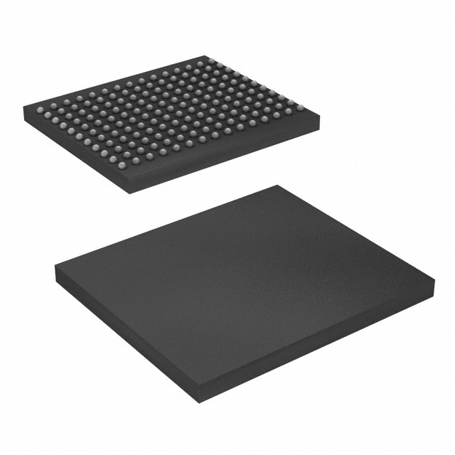
- Part No.:
- CY7C1265KV18-550BZC
- Manufacturer:
- Cypress Semiconductor Corp
- Category:
- Memory
- Package:
- 165-LBGA
- Datasheet:
-
 CY7C1265KV18-550BZC.pdf
- Description:
- IC SRAM 36MBIT PAR 165FBGA
- Quantity:
- Payment:

- Shipping:

Inventory:148
Please send an inquiry. Send us your inquiry, and we will respond immediately.
Product details
Overview
CY7C1265KV18 from Cypress Semiconductor is a 1M × 36, 36-Mbit QDR® II+ SRAM with 2.5-cycle read latency, 550 MHz clock operation (1100 MT/s DDR), 1.8 V core supply, and 1.4–1.8 V I/O supply. It features separate read/write ports, echo clocks (CQ/CQ), QVLD data-valid indicator, and JTAG 1149.1 test access-designed for high-bandwidth packet buffering in network switches and routers.
For engineers reviewing the CY7C1265KV18 datasheet, CY7C1265KV18 pinout, CY7C1265KV18 application, or CY7C1265KV18 equivalent, key selection criteria include burst depth (four 36-bit words), HSTL I/O compatibility, PLL-controlled timing accuracy, and FBGA-165 package thermal/mechanical constraints for dense PCB layouts.
Technical Context
The CY7C1265KV18 implements a synchronous, pipelined QDR II+ architecture with independent read and write ports sharing a multiplexed 18-bit address bus. All inputs are registered on rising edges of K (positive) and K (negative) clocks, enabling true concurrent read/write transactions without bus turnaround.
It uses an internal PLL to align echo clocks (CQ/CQ) with input clocks for precise DDR data capture, and supports programmable output impedance via ZQ pin. DOFF pin selects between 2.5-cycle QDR II+ mode (DOFF = HIGH) and 1-cycle QDR I mode (DOFF = LOW), with corresponding frequency limits (550 MHz vs. 167 MHz).
Key Specifications
| Parameter | Value and Actual Design Meaning |
|---|---|
| Memory Density | 36 Mbit (1M × 36 organization) |
| Max Clock Frequency | 550 MHz - enables 1100 MT/s DDR throughput per port |
| Read Latency | 2.5 clock cycles - deterministic timing for pipeline-aligned data capture |
| Core Supply (VDD) | 1.8 V ± 0.1 V - defines logic threshold and power integrity requirements |
| I/O Supply (VDDQ) | 1.4 V to 1.8 V - supports HSTL Class I/III signaling and system-level voltage scaling |
| Package | 165-ball FBGA (13 × 15 × 1.4 mm) - specifies board layout, thermal pad, and reflow profile |
| Interface Standard | HSTL inputs / variable-drive HSTL outputs - ensures signal integrity at >500 MHz |
Pinout & Package
Package: 165-ball Fine-Pitch Ball Grid Array (FBGA), 13 mm × 15 mm × 1.4 mm body, 0.8 mm ball pitch, RoHS-compliant.
| Pin/Terminal | Circuit Role | Design Meaning |
|---|---|---|
| D[35:0] | Write data inputs | 36-bit synchronous write bus sampled on K/K rising edges; BWS[3:0] controls byte-level write masking |
| Q[35:0] | Read data outputs | 36-bit DDR outputs aligned to CQ/CQ; tristated when RPS is deasserted |
| RPS / WPS | Port select controls | Active-low synchronous enables for read/write ports; decouples port activation from address strobing |
| K / K | Input clocks | Dual-phase clocks drive all synchronous registers; K used for address/RPS/WPS, K for data/BWS |
| CQ / CQ | Echo clocks | Free-running, phase-matched copies of K/K - simplify high-speed source-synchronous capture |
| QVLD | Data validity indicator | Edge-aligned with CQ/CQ; asserts one cycle before valid Q[35:0] data appears |
| ZQ | Impedance calibration input | Connects to external resistor to ground to tune output driver impedance to 0.2 × RQ |
| DOFF | PLL disable control | LOW disables PLL, reverts device to QDR I mode (1-cycle latency, ≤167 MHz) |
Key Features
| Feature | Design Value |
|---|---|
| Four-word burst architecture | Transfers four 36-bit words per access in two clock cycles - reduces address bus toggling by 75% vs. single-word |
| Separate read/write data paths | Eliminates bidirectional bus turnaround delay and contention - enables true concurrent read/write at full bandwidth |
| Synchronous self-timed writes | On-chip write timing control ensures reliable setup/hold margins without external write-strobe generation |
| JTAG 1149.1 boundary scan | Enables IEEE-compliant production testing and interconnect verification in assembled systems |
| Programmable output impedance | ZQ-based calibration matches driver strength to PCB trace impedance - improves signal integrity at 1100 MT/s |
Applications
| Network Packet Buffering | High-Speed Test Equipment Memory |
|---|---|
|
Use Scenario: Storing ingress/egress packet headers and payloads in Layer 2/3 switching ASICs with real-time traffic shaping. IC Role / Device Role / Timing Role: Dedicated burst-access SRAM providing deterministic 2.5-cycle read latency and concurrent write capability for backpressure management. Use Value: Enables line-rate forwarding at 10 Gbps+ by sustaining 1100 MT/s per port without arbitration stalls or bus turnaround overhead. |
Use Scenario: Capturing high-fidelity waveform samples in automated test equipment (ATE) with nanosecond-level timestamp alignment. IC Role / Device Role / Timing Role: High-throughput buffer interfacing directly to ADC/DAC controllers using HSTL signaling and echo-clock–synchronized capture. Use Value: Delivers consistent 550 MHz timing margin across temperature/voltage, supporting sub-2 ns sampling jitter in production test environments. |
| Telecom Line Card Buffering | Real-Time Video Frame Buffering |
|
Use Scenario: Temporary storage of ATM/SONET cell payloads and OAM cells in carrier-grade optical line cards. IC Role / Device Role / Timing Role: Low-latency, depth-expandable memory supporting multi-port expansion via RPS/WPS and BWS[3:0] granularity. Use Value: Allows seamless 1M × 36 → 2M × 36 expansion using port-select logic - avoids redesign when bandwidth demand increases. |
Use Scenario: Intermediate frame storage in broadcast-grade video encoders handling 4K60 YUV422 streams with minimal latency. IC Role / Device Role / Timing Role: Dual-port burst SRAM supplying pixel data to encoder pipelines while accepting compressed output from previous frames. Use Value: Sustains 8.8 GB/s aggregate bandwidth (1100 MT/s × 8 bytes) required for dual 4K60 streams without frame drops or FIFO overflow. |
Equivalent & Alternatives
The following parts are listed as comparable options for similar high-bandwidth burst SRAM applications.
| Alternative Part | Technical Difference | Application Difference | Selection Advice |
|---|---|---|---|
| AS7C336518B-550BIN | Same 1M × 36 density and 550 MHz speed, but uses SSTL-15 I/O (1.5 V only), no ZQ calibration, no DOFF mode switch | Limited to 1.5 V systems; lacks QDR II+ PLL flexibility and echo-clock timing aid for >500 MHz capture | Prefer when cost-sensitive and system already uses SSTL-15; avoid if VDDQ scaling or QDR I fallback is needed |
| IS42S32800J-5BL | SDRAM-based (not QDR), 256M × 32, 533 MHz clock, 1.8 V only, asynchronous refresh, no separate ports | Higher density but higher latency (CAS latency ≥3), requires refresh management and bus arbitration | Only suitable where burst depth >4 and latency tolerance >10 ns exist; not drop-in for QDR II+ designs |
Compared with AS7C336518B-550BIN and IS42S32800J-5BL, the CY7C1265KV18 uniquely delivers deterministic 2.5-cycle latency, true concurrent access, and hardware-assisted timing (CQ/QVLD/ZQ) essential for deterministic high-speed packet and sample buffering.
Availability
CY7C1265KV18 is available at Aetrix Electronics and suitable for network switching, telecom line cards, high-speed test instrumentation, and broadcast video processing requiring stable component supply across extended product lifecycles.
Supply support for CY7C1265KV18 includes scheduled delivery planning, volume procurement assistance, BOM continuity management, traceable sourcing, and lifecycle availability coordination for OEM customers, industrial embedded developers, connected-device designers, and electronics production programs.
Manufacturer
Cypress Semiconductor (now part of Infineon Technologies) is a fabless semiconductor company specializing in high-performance memory, microcontrollers, and connectivity solutions for industrial, automotive, and communications markets.
The CY7C1265KV18 belongs to Cypress's QDR® II+ SRAM product line, engineered specifically for deterministic, low-latency, high-throughput buffering in infrastructure equipment where bus turnaround overhead and timing uncertainty must be eliminated.
FAQ
What is the function of the DOFF pin, and how does it affect timing?
The DOFF pin disables the internal PLL when driven LOW, reverting the CY7C1265KV18 to QDR I mode with 1-cycle read latency and maximum 167 MHz operation. When HIGH, the PLL enables 2.5-cycle latency and full 550 MHz performance. This dual-mode capability allows backward compatibility with legacy QDR I designs while supporting next-generation bandwidth demands.
How do CQ and CQ echo clocks improve system timing margin?
CQ and CQ are free-running, phase-aligned copies of K and K clocks, respectively, routed alongside Q[35:0] outputs. They provide a local, low-skew reference for capturing DDR data at the receiver, eliminating clock-to-data skew caused by PCB trace length mismatches. This directly improves setup/hold timing margins at 1100 MT/s, especially in multi-drop or long-trace configurations.
Can the CY7C1265KV18 be used with 1.5 V VDDQ only?
Yes. The device supports VDDQ from 1.4 V to 1.8 V, including 1.5 V nominal. At 1.5 V, it meets all AC/DC specifications for HSTL Class I and III interfaces, and maintains full 550 MHz operation. No configuration change is required-only ensure VDDQ supply stability within ±3% and proper decoupling per the datasheet layout guidelines.
What is the role of the ZQ pin, and how should it be connected?
ZQ enables output driver impedance calibration. It must be connected to a precision resistor (typically 240 Ω) tied to ground, setting output impedance to 48 Ω (0.2 × 240 Ω). Alternatively, connecting ZQ directly to VDDQ enables minimum-impedance mode (~24 Ω). ZQ must never be left floating or tied to ground, as this disables calibration and risks signal integrity failure at high speeds.
CY7C1265KV18-550BZC Specifications
- Product attributes
- Attribute value
- Manufacturer:
- Cypress Semiconductor Corp
- Series:
- -
- Package/Case:
- 165-LBGA
- Packaging:
- Bulk
- Product Status:
- Active
- Programmable:
- Not Verified
- Memory Type:
- Volatile
- Memory Format:
- SRAM
- Technology:
- SRAM - Synchronous, QDR II+
- Memory Size:
- 36Mbit
- Memory Organization:
- 1M x 36
- Memory Interface:
- Parallel
- Clock Frequency:
- 550 MHz
- Write Cycle Time - Word, Page:
- -
- Access Time:
- -
- Voltage - Supply:
- 1.7V ~ 1.9V
- Operating Temperature:
- 0°C ~ 70°C (TA)
- Grade:
- -
- Qualification:
- -
- Mounting Type:
- Surface Mount
- Supplier Device Package:
- 165-FBGA (13x15)
CY7C1265KV18-550BZC FAQ
1.How can I place an order for CY7C1265KV18-550BZC through Aetrix?
Please submit a Request for Quotation (RFQ) for CY7C1265KV18-550BZC on Aetrix. Our sales agent will provide a competitive quotation and guide you through the order confirmation once you accept the terms.
2.Are the price and stock information for CY7C1265KV18-550BZC reliable?
The price and inventory of CY7C1265KV18-550BZC are updated periodically and may fluctuate due to market conditions. Stock and pricing data are typically refreshed every 24 hours. Quotation validity for CY7C1265KV18-550BZC is usually 5 days.
3.What payment methods are accepted for CY7C1265KV18-550BZC?
We accept Wire Transfer, PayPal, Credit Card, Western Union, MoneyGram, and Escrow for CY7C1265KV18-550BZC transactions.
Note: Certain payment methods may incur a processing fee.
4.How is shipping managed for CY7C1265KV18-550BZC?
CY7C1265KV18-550BZC orders can be shipped via leading logistics carriers, including DHL, UPS, FedEx, TNT, or Registered Mail.
Once your CY7C1265KV18-550BZC order is processed, you will receive an email with the shipment details and tracking number.
Note: Tracking information may take up to 24 hours to appear. Express delivery typically takes 3–5 business days.
5.How can I obtain technical support or documentation for CY7C1265KV18-550BZC?
For technical support, including CY7C1265KV18-550BZC datasheets, pinout diagrams, or application guidance, please contact our engineering support team. They can provide detailed documentation and assistance for your CY7C1265KV18-550BZC requirements.
6.How does Aetrix verify that CY7C1265KV18-550BZC is sourced from the original manufacturer or authorized distributors?
All CY7C1265KV18-550BZC products on Aetrix are procured from qualified distributors and authorized channels. Our dedicated quality assurance team conducts strict verification, including traceability checks and, if necessary, third-party testing. This ensures that CY7C1265KV18-550BZC meets industry standards.
7.What is the process for return or replacement of CY7C1265KV18-550BZC?
All CY7C1265KV18-550BZC units undergo pre-shipment inspection (PSI). If there is an issue with CY7C1265KV18-550BZC, returns or replacements are accepted under the following conditions:
1.Quantity discrepancies, incorrect items, or visible external defects (such as breakage or corrosion), acknowledged by Aetrix.
2.The issue is reported within 90 days of delivery.
3.The CY7C1265KV18-550BZC part is unused and in its original packaging.
Return procedure for CY7C1265KV18-550BZC:
1.Submit a request within 90 days.
2.Obtain a Return Material Authorization (RMA) from Aetrix.
CY7C1265KV18-550BZC Tags

-
M24C02-WMN6TP
STMicroelectronics

-
AT24C02C-XHM-T
Microchip Technology

-
AT21CS01-STUM10-T
Microchip Technology

-
AT24C02C-SSHM-T
Microchip Technology

-
24LC01BT-I/OT
Microchip Technology

-
M24C02-FMC6TG
STMicroelectronics
-
AT24CS02-SSHM-T
Microchip Technology

-
93LC46BT-I/OT
Microchip Technology
-
AT24C04C-SSHM-T
Microchip Technology

-
24LC01BT-I/SN
Microchip Technology
-
24AA02UIDT-I/OT
Microchip Technology

-
AT24C08C-STUM-T
Microchip Technology
Tech Hub

18650 battery guide covering lithium-ion cell basics, 3.6V/3.7V voltage, 4.2V charging, mAh and Wh capacity, protected cells, chargers, BMS, series-parallel packs, holders, welding and sourcing checks.…

Hall effect sensor guide covering working principle, linear and digital sensors, Arduino circuits, current sensing, speed detection, automotive applications, A3144 examples, signal filtering and datash…

Product Change Notification guide for electronic components, covering PCN meaning, PCN vs PDN/EOL, common change types, risk levels, form-fit-function review, engineering validation, BOM control, LTB/L…

A practical guide to blend door actuators, covering HVAC function, symptoms, location, AC and heater issues, reset and calibration, replacement cost, electrical diagnosis, compatibility checks, and rep…

Engineering guide to Raspberry Pi alternatives, covering chip-level differences, Orange Pi, ROCK, Jetson, Banana Pi, NanoPi, Compute Module, Pico, GPIO, camera, HAT compatibility, and replacement risks…

Engineering guide to dynamic load response testing for high-current buck converters, covering load step setup, slew rate, Vcore undershoot, overshoot, recovery time, probe location, output capacitors a…

Engineering guide to output capacitor selection for ASIC Vcore rails, covering bulk capacitors, polymer capacitors, MLCC decoupling, DC bias, ESR, ESL, placement, transient response and substitution ri…

Engineering guide to high-current ASIC Vcore rails, covering 12-phase buck architecture, PMBus control, dynamic load testing, output capacitor networks, smart power stage selection, thermal design and …

Voltage regulator guide covering linear, LDO, 7805, Zener, adjustable, buck, VRM and alternator regulators, with design checks, testing methods, troubleshooting and datasheet-based selection.

Amplifier guide covering voltage, current and power amplification, gain, feedback, amplifier classes, audio and RF applications, op-amp circuits, transimpedance amplifiers, datasheet selection and trou…


