
 My Inquiry
 My Account


Cypress Semiconductor Corp CY7C1470BV25-167BZXC
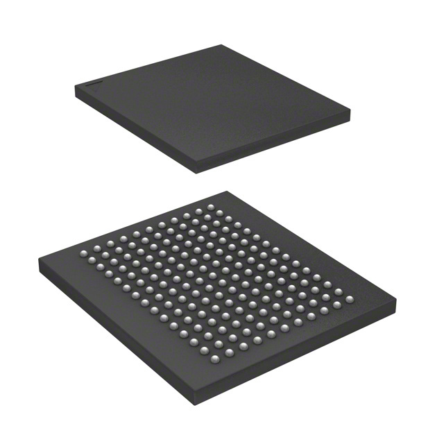
- Part No.:
- CY7C1470BV25-167BZXC
- Manufacturer:
- Cypress Semiconductor Corp
- Category:
- Memory
- Package:
- 165-LBGA
- Datasheet:
-
 CY7C1470BV25-167BZXC.pdf
- Description:
- IC SRAM 72MBIT PAR 165FBGA
- Quantity:
- Payment:

- Shipping:

Inventory:190
Please send an inquiry. Send us your inquiry, and we will respond immediately.
Product details
Overview
CY7C1470BV25-167BZXC from Cypress Semiconductor is a 72-Mbit (2M × 36) synchronous pipelined SRAM with NoBL™ architecture, designed for high-throughput memory buffering in network packet processors and telecom line cards. It operates at 167 MHz with 3.4 ns maximum access time, supports zero-wait-state back-to-back reads/writes, and uses single 2.5V VDD with separate 2.5V VDDQ I/O supply.
For engineers reviewing the CY7C1470BV25-167BZXC datasheet, CY7C1470BV25-167BZXC pinout, CY7C1470BV25-167BZXC application, or CY7C1470BV25-167BZXC equivalent, key selection criteria include burst order configuration (linear/interleaved), byte-write select granularity (BWa–BWd), synchronous self-timed write timing, and JEDEC-compliant 100-pin TQFP packaging with JTAG boundary scan support.
Technical Context
This SRAM implements fully registered pipelined operation: all address, control, and data inputs are latched on the rising edge of CLK, and all outputs are driven from output registers synchronized to CLK. The internal NoBL™ logic eliminates bus latency by enabling consecutive read/write cycles without wait states.
It features three synchronous chip enables (CE1 active-low, CE2 active-high, CE3 active-low), asynchronous OE for tri-state control, Clock Enable (CEN) for cycle extension, and ADV/LD to load or advance the burst counter. Burst order (linear or interleaved) is set by the MODE strap pin, which must remain static during operation.
Key Specifications
| Parameter | Value and Actual Design Meaning |
|---|---|
| Memory Density | 72 Mbit (2M × 36 organization), enabling 9 MB of fast buffer storage per device |
| Max Clock Frequency | 167 MHz - supports sustained 167 MT/s throughput with no wait states |
| Access Time (tCO) | 3.4 ns - defines maximum clock-to-output delay for timing-critical read paths |
| Supply Voltages | VDD = 2.5V ±0.2V, VDDQ = 2.5V ±0.2V - dual-rail I/O allows clean signal integrity in mixed-voltage systems |
| Burst Capability | Linear or interleaved 4-word burst - reduces address bus traffic and improves bandwidth efficiency |
| Byte Write Control | Four independent BWa–BWd signals - enables selective 9-bit writes to DQa/DQPa through DQd/DQPd |
| Power Consumption | 400 mA max operating current, 120 mA CMOS standby - suitable for thermally constrained telecom modules |
Pinout & Package
Package: 100-pin TQFP (14 × 14 mm, 0.5 mm pitch), RoHS-compliant Pb-free, JEDEC-standard footprint.
| Pin/Terminal | Circuit Role | Design Meaning |
|---|---|---|
| A0–A18 | Synchronous Address Input | Latched on rising CLK edge; selects one of 2M addresses in 2M × 36 mode |
| BWa–BWd | Synchronous Byte Write Select | Active-low controls 9-bit write segments: BWa→DQa/DQPa, BWb→DQb/DQPb, etc. |
| CE1, CE3 | Synchronous Chip Enable (active-low) | Combined with CE2 (active-high) for 3-signal depth expansion and bank isolation |
| CLK, CEN | Clock and Clock Enable | CEN masks CLK without deselecting device - enables precise cycle extension for timing alignment |
| DQa–DQd, DQPa–DQPd | Bidirectional Data I/O | 36-bit data + 4-bit parity; automatically tri-stated during write data phase to prevent bus contention |
| OE | Asynchronous Output Enable | Tri-states outputs when HIGH; masked during write sequences and device deselection to ensure safe bus handoff |
| MODE | Strap Pin | Static configuration of burst order: HIGH = interleaved, LOW = linear; floating defaults to HIGH |
| ADV/LD | Advance/Load Control | LOW loads new address; HIGH advances internal burst counter - enables seamless burst sequencing |
Key Features
| Feature | Design Value |
|---|---|
| No Bus Latency™ (NoBL™) Architecture | Enables true back-to-back read/write operations with zero wait states, delivering sustained 167 MT/s throughput |
| Fully Registered Pipelined Interface | All inputs and outputs synchronized to CLK rising edge - simplifies timing closure in high-speed FPGA/ASIC interfaces |
| Synchronous Self-Timed Writes | On-chip write timing control eliminates external write pulse width constraints and reduces PCB routing complexity |
| JTAG Boundary Scan (IEEE 1149.1) | Supports in-system testability and interconnect verification without additional test fixtures or probes |
| Flexible Burst and Byte-Write Granularity | Configurable 4-word burst order + independent 9-bit byte writes - optimizes bandwidth and data integrity in packet buffer applications |
Applications
| Network Packet Buffering | Telecom Line Card Memory |
|---|---|
|
Use Scenario: Storing and forwarding variable-length Ethernet/IP packets in Layer 2/3 switches. IC Role / Device Role / Timing Role: High-speed, low-latency buffer SRAM interfacing directly with packet processor's 36-bit data bus. Use Value: 167 MHz zero-wait-state operation ensures full line-rate packet buffering without stalling the processor pipeline. |
Use Scenario: Frame buffering in OC-192/STM-64 SONET/SDH line interface cards. IC Role / Device Role / Timing Role: Synchronous burst-access memory for ATM cell or GFP frame assembly/disassembly engines. Use Value: Interleaved burst mode aligns with SONET's time-division multiplexing structure, reducing address overhead by 75%. |
| Baseband Processing Buffer | Radar Signal Processing FIFO |
|
Use Scenario: Temporary storage of IQ samples between digital down-conversion and channel decoding in LTE eNodeB basebands. IC Role / Device Role / Timing Role: Dual-port-capable SRAM used as ping-pong buffer with FPGA controller managing CE1/CE2 bank switching. Use Value: Byte-write capability (BWa–BWd) enables efficient partial updates of complex sample buffers without full-word overwrites. |
Use Scenario: Real-time buffering of ADC samples prior to FFT processing in phased-array radar front ends. IC Role / Device Role / Timing Role: Low-jitter, deterministic-access memory providing continuous 167 MT/s streaming to DSP DMA engines. Use Value: 3.4 ns tCO and fully registered interface minimize timing uncertainty in sample-to-FFT latency budgets. |
Equivalent & Alternatives
The following parts are listed as comparable options for similar synchronous burst SRAM applications.
| Alternative Part | Technical Difference | Application Difference | Selection Advice |
|---|---|---|---|
| IDT72V2115L10PF | 36-Mbit (1M × 36), 10 ns access, 100 MHz max frequency, 3.3V core/I/O | Lower density and speed; suited for legacy 3.3V systems with relaxed timing margins | Select when migrating older ZBT designs with 3.3V infrastructure and no need for >133 MHz operation |
| ISSI IS61WV102436B | 36-Mbit (1M × 36), 2.5V core/I/O, 167 MHz, but lacks NoBL™ and burst counter - requires external address generation | No internal burst logic; requires FPGA to manage sequential addressing - increases logic utilization and latency | Choose only if cost sensitivity outweighs performance and design simplicity; verify FPGA resource availability for burst address gen |
Compared with IDT72V2115L10PF and IS61WV102436B, CY7C1470BV25-167BZXC delivers double the density, 67% higher throughput, and integrated burst/byte-write control - reducing system-level timing risk and FPGA logic burden in next-gen packet processing.
Availability
CY7C1470BV25-167BZXC is available at Aetrix Electronics and suitable for network packet processors, telecom line cards, and radar signal processors requiring stable component supply, long-lifecycle support, and RoHS-compliant 100-pin TQFP packaging.
Supply support for CY7C1470BV25-167BZXC includes scheduled delivery planning, volume procurement assistance, BOM continuity management, traceable sourcing, and lifecycle availability coordination for OEM customers, industrial embedded developers, connected-device designers, and electronics production programs.
Manufacturer
Cypress Semiconductor (now part of Infineon Technologies) is a fabless semiconductor company specializing in high-performance memory, microcontrollers, and programmable logic solutions for industrial, automotive, and communications markets.
CY7C1470BV25 belongs to Cypress's NoBL™ SRAM product line, engineered specifically for zero-latency, high-bandwidth buffering in real-time data-path applications such as packet switching, baseband processing, and high-speed test equipment.
FAQ
What is the function of the MODE pin, and how must it be configured?
The MODE pin is a static strap input that selects burst order: pulled HIGH for interleaved burst, LOW for linear burst. It must be held stable during operation - floating defaults to HIGH (interleaved). This setting determines how the internal burst counter increments addresses and cannot be changed dynamically during active bursts.
How does the CY7C1470BV25-167BZXC handle bus contention during write cycles?
During the data portion of a write sequence, the device automatically tri-states all DQ and DQP outputs regardless of OE state - preventing bus contention without requiring external bus arbitration logic. This behavior is hardwired in the NoBL™ control logic and occurs synchronously with the write data capture clock edge.
Can CE2 be used as an active-low enable like CE1 and CE3?
No - CE2 is defined as active-HIGH per the datasheet and pin definition table. Using it as active-low would violate the device's synchronous enable protocol and may cause undefined behavior or failed accesses. CE1 and CE3 must both be active-low, while CE2 must be active-high for proper chip selection.
Is the ZZ Sleep Mode supported in the CY7C1470BV25-167BZXC variant?
Yes - the ZZ pin is present and functional in the 100-pin TQFP package (Pin 81), enabling hardware-controlled deep sleep mode to reduce standby current. When asserted LOW, ZZ places the device in low-power state with retention of memory contents; recovery time is specified as 20 ns max after ZZ deassertion.
CY7C1470BV25-167BZXC Specifications
- Product attributes
- Attribute value
- Manufacturer:
- Cypress Semiconductor Corp
- Series:
- NoBL™
- Package/Case:
- 165-LBGA
- Packaging:
- Tray
- Product Status:
- Obsolete
- Programmable:
- Not Verified
- Memory Type:
- Volatile
- Memory Format:
- SRAM
- Technology:
- SRAM - Synchronous, SDR
- Memory Size:
- 72Mbit
- Memory Organization:
- 2M x 36
- Memory Interface:
- Parallel
- Clock Frequency:
- 167 MHz
- Write Cycle Time - Word, Page:
- -
- Access Time:
- 3.4 ns
- Voltage - Supply:
- 2.375V ~ 2.625V
- Operating Temperature:
- 0°C ~ 70°C (TA)
- Grade:
- -
- Qualification:
- -
- Mounting Type:
- Surface Mount
- Supplier Device Package:
- 165-FBGA (15x17)
CY7C1470BV25-167BZXC FAQ
1.How can I place an order for CY7C1470BV25-167BZXC through Aetrix?
Please submit a Request for Quotation (RFQ) for CY7C1470BV25-167BZXC on Aetrix. Our sales agent will provide a competitive quotation and guide you through the order confirmation once you accept the terms.
2.Are the price and stock information for CY7C1470BV25-167BZXC reliable?
The price and inventory of CY7C1470BV25-167BZXC are updated periodically and may fluctuate due to market conditions. Stock and pricing data are typically refreshed every 24 hours. Quotation validity for CY7C1470BV25-167BZXC is usually 5 days.
3.What payment methods are accepted for CY7C1470BV25-167BZXC?
We accept Wire Transfer, PayPal, Credit Card, Western Union, MoneyGram, and Escrow for CY7C1470BV25-167BZXC transactions.
Note: Certain payment methods may incur a processing fee.
4.How is shipping managed for CY7C1470BV25-167BZXC?
CY7C1470BV25-167BZXC orders can be shipped via leading logistics carriers, including DHL, UPS, FedEx, TNT, or Registered Mail.
Once your CY7C1470BV25-167BZXC order is processed, you will receive an email with the shipment details and tracking number.
Note: Tracking information may take up to 24 hours to appear. Express delivery typically takes 3–5 business days.
5.How can I obtain technical support or documentation for CY7C1470BV25-167BZXC?
For technical support, including CY7C1470BV25-167BZXC datasheets, pinout diagrams, or application guidance, please contact our engineering support team. They can provide detailed documentation and assistance for your CY7C1470BV25-167BZXC requirements.
6.How does Aetrix verify that CY7C1470BV25-167BZXC is sourced from the original manufacturer or authorized distributors?
All CY7C1470BV25-167BZXC products on Aetrix are procured from qualified distributors and authorized channels. Our dedicated quality assurance team conducts strict verification, including traceability checks and, if necessary, third-party testing. This ensures that CY7C1470BV25-167BZXC meets industry standards.
7.What is the process for return or replacement of CY7C1470BV25-167BZXC?
All CY7C1470BV25-167BZXC units undergo pre-shipment inspection (PSI). If there is an issue with CY7C1470BV25-167BZXC, returns or replacements are accepted under the following conditions:
1.Quantity discrepancies, incorrect items, or visible external defects (such as breakage or corrosion), acknowledged by Aetrix.
2.The issue is reported within 90 days of delivery.
3.The CY7C1470BV25-167BZXC part is unused and in its original packaging.
Return procedure for CY7C1470BV25-167BZXC:
1.Submit a request within 90 days.
2.Obtain a Return Material Authorization (RMA) from Aetrix.
CY7C1470BV25-167BZXC Tags

-
M24C02-WMN6TP
STMicroelectronics

-
AT24C02C-XHM-T
Microchip Technology

-
AT21CS01-STUM10-T
Microchip Technology

-
AT24C02C-SSHM-T
Microchip Technology

-
24LC01BT-I/OT
Microchip Technology

-
M24C02-FMC6TG
STMicroelectronics
-
AT24CS02-SSHM-T
Microchip Technology

-
93LC46BT-I/OT
Microchip Technology
-
AT24C04C-SSHM-T
Microchip Technology

-
24LC01BT-I/SN
Microchip Technology
-
24AA02UIDT-I/OT
Microchip Technology

-
AT24C08C-STUM-T
Microchip Technology
Tech Hub

Product Change Notification guide for electronic components, covering PCN meaning, PCN vs PDN/EOL, common change types, risk levels, form-fit-function review, engineering validation, BOM control, LTB/L…

A practical guide to blend door actuators, covering HVAC function, symptoms, location, AC and heater issues, reset and calibration, replacement cost, electrical diagnosis, compatibility checks, and rep…

Engineering guide to Raspberry Pi alternatives, covering chip-level differences, Orange Pi, ROCK, Jetson, Banana Pi, NanoPi, Compute Module, Pico, GPIO, camera, HAT compatibility, and replacement risks…

Engineering guide to dynamic load response testing for high-current buck converters, covering load step setup, slew rate, Vcore undershoot, overshoot, recovery time, probe location, output capacitors a…

Engineering guide to output capacitor selection for ASIC Vcore rails, covering bulk capacitors, polymer capacitors, MLCC decoupling, DC bias, ESR, ESL, placement, transient response and substitution ri…

Engineering guide to high-current ASIC Vcore rails, covering 12-phase buck architecture, PMBus control, dynamic load testing, output capacitor networks, smart power stage selection, thermal design and …

Voltage regulator guide covering linear, LDO, 7805, Zener, adjustable, buck, VRM and alternator regulators, with design checks, testing methods, troubleshooting and datasheet-based selection.

Amplifier guide covering voltage, current and power amplification, gain, feedback, amplifier classes, audio and RF applications, op-amp circuits, transimpedance amplifiers, datasheet selection and trou…

Machine vision system guide covering components, inspection workflow, camera and lens selection, FOV, pixel resolution, motion blur, strobe lighting, bandwidth, 2D/3D vision, integration, troubleshooti…

Electronic devices and circuits guide covering passive components, semiconductors, analog and digital circuits, circuit theory, practical calculations, troubleshooting, datasheet selection, and learnin…


