
 My Inquiry
 My Account


Infineon Technologies CY8C3845PVE-173
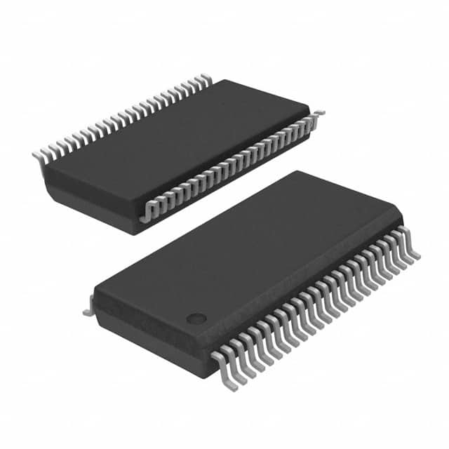
- Part No.:
- CY8C3845PVE-173
- Manufacturer:
- Infineon Technologies
- Category:
- Microcontrollers
- Package:
- 48-BSSOP (0.295", 7.50mm Width)
- Datasheet:
-
 CY8C3845PVE-173.pdf
- Description:
- IC MCU 8BIT 32KB FLASH 48SSOP
- Quantity:
- Payment:

- Shipping:

Inventory:3,786
Please send an inquiry. Send us your inquiry, and we will respond immediately.
Product details
Overview
CY8C3845PVE-173 from Infineon Technologies (formerly Cypress) is an AEC-Q100 qualified automotive-grade PSoC® 3 programmable system-on-chip integrating an 8051 CPU core, up to 64 KB flash, 8 KB SRAM, 2 KB EEPROM, 24-channel DMA, and configurable analog/digital peripherals including CAN 2.0b, USB 2.0 Full-Speed, delta-sigma ADC (20-bit, 192 ksps), four opamps, and CapSense®. It operates from 1.71 V to 5.5 V across –40 °C to +85 °C and targets embedded control in body electronics, sensor fusion, and powertrain interface modules.
For engineers reviewing the CY8C3845PVE-173 datasheet, CY8C3845PVE-173 pinout, CY8C3845PVE-173 application, or CY8C3845PVE-173 equivalent, key selection criteria include AEC-Q100 compliance, integrated CAN/USB connectivity, programmable analog blocks (PGA/TIA), low-power hibernate mode (200 nA), and PSoC Creator™-based firmware reconfigurability without hardware changes.
Technical Context
The CY8C3845PVE-173 implements a single-cycle 8051 microcontroller core with up to 67 MHz operation, supported by a multilayer AHB bus, 24-channel DMA, and programmable universal digital blocks (UDBs) for custom logic synthesis. Its analog subsystem centers on a 1.024 V ±0.1% internal reference and a configurable delta-sigma ADC with selectable gain (×0.25–×16) and resolution (8–20 bit).
Digital peripheral integration includes full CAN 2.0b controller (16 Rx/8 Tx buffers), USB 2.0 FS PHY (TID#40770053 certified), four 16-bit timer/counter/PWM blocks, and a 24-bit digital filter block (DFB) supporting FIR/IIR filtering. All I/O routing is fully configurable via DSI, enabling any GPIO to connect to any analog or digital resource.
Key Specifications
| Parameter | Value and Actual Design Meaning |
|---|---|
| CPU Core | Single-cycle 8051 running up to 67 MHz - enables deterministic real-time control with minimal instruction latency. |
| Memory | 64 KB flash (100k write cycles, 20-yr retention), 8 KB SRAM, 2 KB EEPROM - supports field-upgradable firmware and persistent calibration data storage. |
| Analog ADC | Delta-sigma ADC: 20-bit resolution, 192 ksps max, 66 dB SINAD @12-bit - delivers high-accuracy sensor signal acquisition for thermocouples or pressure transducers. |
| Digital Interfaces | CAN 2.0b (16 Rx/8 Tx buffers), USB 2.0 Full-Speed (12 Mbps), I²C multimaster - enables direct vehicle network and PC communication without external transceivers. |
| Power Management | 1.71–5.5 V supply range; 200 nA hibernate mode with RAM retention - sustains battery-backed operation in always-on automotive modules. |
| Temperature Range | –40 °C to +85 °C, AEC-Q100 Grade 2 qualified - validated for under-hood and cabin-mounted automotive ECUs. |
| I/O Count | 62 GPIOs + 8 SIOs + 2 USBIOs in 100-pin TQFP - provides scalable routing for mixed-signal sensor aggregation and actuator control. |
Pinout & Package
Package: 100-pin Thin Quad Flat Package (TQFP), RoHS-compliant, lead-free, body size 14 mm × 14 mm, 0.5 mm pitch.
| Pin/Terminal | Circuit Role | Design Meaning |
|---|---|---|
| VDDIO0–VDDIO3 | I/O Power Domains | Four independent 1.2–5.5 V I/O voltage rails - enables mixed-voltage interfacing (e.g., 3.3 V MCU logic + 5 V analog sensors). |
| P0[0]–P7[7] | General-Purpose I/O | 62 fully routable GPIOs with Schmitt-trigger inputs, configurable pull-up/down, open-drain, or strong drive - supports CapSense®, LCD segment drive, and digital peripheral mapping. |
| USB_DP / USB_DM | USB 2.0 Full-Speed Interface | Differential pair routed to internal USB PHY - eliminates need for external USB transceiver in diagnostic or firmware update interfaces. |
| CAN_TX / CAN_RX | CAN 2.0b Physical Layer Interface | Dedicated differential pins connected to internal CAN controller - requires external CAN transceiver (e.g., TJA1042) for bus coupling. |
| XRES | External Reset Input | Active-low asynchronous reset pin - allows system-level fault recovery independent of internal watchdog or power-on reset timing. |
Key Features
| Feature | Design Value |
|---|---|
| Configurable UDB Array (24 blocks) | Each UDB combines PLD logic + state machine - enables custom protocol engines (e.g., LIN slave, SPI-to-I²C bridge) without FPGA or external logic. |
| CapSense® on Any GPIO | Self- and mutual-capacitance sensing using dedicated hardware - supports touch buttons, sliders, and proximity detection with <10 µA active current. |
| Digital Filter Block (DFB) | 24-bit fixed-point engine for real-time FIR/IIR filtering - processes ultrasonic echo signals or motor current harmonics at 67 MHz clock rate. |
| Programmable Analog Blocks | Four SC/CT-based blocks configurable as PGA, TIA, mixer, or sample-and-hold - replaces discrete opamp networks for current/voltage sensing front-ends. |
| Secure Bootloader Support | Firmware updates via UART, I²C, SPI, or USB with flash protection - prevents unauthorized code execution during over-the-air or service-bay reprogramming. |
Applications
| Automotive Body Control Module | Smart Sensor Hub |
|---|---|
Use Scenario: Centralized control of door locks, window lifts, mirrors, and interior lighting in modern vehicles. IC Role / Device Role / Timing Role: Main MCU executing CAN message arbitration, PWM motor control, and CapSense® touch interface management. Use Value: Integrates 62 GPIOs, CAN 2.0b, and CapSense® into one die - reduces BOM count by eliminating separate touch controller and CAN transceiver support ICs. |
Use Scenario: Aggregation and preprocessing of temperature, pressure, and humidity sensor data for HVAC or ADAS thermal monitoring. IC Role / Device Role / Timing Role: Signal acquisition node performing delta-sigma ADC sampling, digital filtering (DFB), and CAN packet formatting. Use Value: 20-bit ADC + programmable PGA enables direct connection to millivolt-level thermopile outputs - avoids external signal conditioning amplifiers. |
| Engine Control Interface Unit | Electric Power Steering (EPS) Monitor |
Use Scenario: Secondary ECU handling throttle position feedback, coolant level sensing, and diagnostic LED drivers. IC Role / Device Role / Timing Role: Real-time sensor interface with 200 nA hibernate mode and wake-on-CAN capability. Use Value: Ultra-low hibernate current extends battery life in parked-vehicle diagnostics - meets OEM requirements for <1 µA total module sleep current. |
Use Scenario: Torque sensor signal conditioning and fault detection in EPS systems requiring functional safety awareness. IC Role / Device Role / Timing Role: Analog front-end with dual-opamp TIA configuration and redundant ADC sampling paths. Use Value: Four uncommitted opamps + 20-bit ADC allow dual-path torque measurement - supports ASIL-B decomposition without external redundancy ICs. |
Equivalent & Alternatives
The following parts are listed as comparable options for similar programmable SoC applications.
| Alternative Part | Technical Difference | Application Difference | Selection Advice |
|---|---|---|---|
| NXP S32K144 | ARM Cortex-M4F core, 160 MHz, no integrated CapSense® or DFB; requires external ADC for >16-bit precision. | Targets higher-performance ASIL-B safety-critical functions (e.g., motor control); lacks native capacitive sensing. | Select when needing ISO 26262 ASIL-B certification out-of-box and ARM ecosystem tooling. |
| Renesas RL78/F14 | 16-bit RL78 core, 32 MHz, integrated 12-bit ADC only, no CAN FD or USB; lower memory density (up to 512 KB flash). | Better suited for cost-sensitive, low-complexity body electronics where USB/CapSense® are unnecessary. | Select for legacy 12 V battery-powered modules with strict cost targets and no need for analog configurability. |
Compared with NXP S32K144 and Renesas RL78/F14, CY8C3845PVE-173 uniquely combines automotive-grade programmable analog (PGA/TIA/ADC), CapSense®, and USB+CAN in one die - reducing component count and layout complexity for mid-tier automotive ECUs where flexibility and integration outweigh raw compute throughput.
Availability
CY8C3845PVE-173 is available at Aetrix Electronics and suitable for automotive body control modules, smart sensor hubs, engine interface units, and electric power steering monitors requiring stable component supply and long-term lifecycle support.
Supply support for CY8C3845PVE-173 includes scheduled delivery planning, volume procurement assistance, BOM continuity management, traceable sourcing, and lifecycle availability coordination for OEM customers, industrial embedded developers, connected-device designers, and electronics production programs.
Manufacturer
Infineon Technologies is a global semiconductor leader headquartered in Munich, Germany, specializing in power management, automotive MCUs, and security solutions with vertical integration from silicon to system-level software.
CY8C3845PVE-173 belongs to the PSoC® 3 automotive family - designed specifically for AEC-Q100-compliant embedded control applications demanding mixed-signal integration, field-upgradable firmware, and low-power operation in harsh environments.
FAQ
Is CY8C3845PVE-173 pin-compatible with other CY8C38 family members?
Yes - CY8C3845PVE-173 uses the 100-pin TQFP package shared across CY8C38xx-17x variants. Pin functions are consistent per datasheet Table 2-1, though peripheral enablement (e.g., USB, CAN) depends on specific part number configuration. No PCB redesign is needed when migrating within the same package option.
Does CY8C3845PVE-173 support functional safety standards like ISO 26262?
CY8C3845PVE-173 is AEC-Q100 Grade 2 qualified and includes hardware features supporting ASIL-B decomposition - such as ECC on flash/SRAM, lockable debug ports, and dual-watchdog timers. However, it is not pre-certified to ISO 26262; customers must perform their own safety analysis and qualification per system requirements.
Can the internal oscillator meet USB Full-Speed timing accuracy requirements?
Yes - the internal main oscillator (IMO) is factory-trimmed to ±2% over temperature and voltage, sufficient for USB Full-Speed (12 Mbps) operation without an external crystal. The datasheet confirms TID#40770053 certification using the IMO, eliminating BOM cost and board space for a 12 MHz crystal.
What development tools are required to program and debug CY8C3845PVE-173?
PSoC Creator™ IDE (v4.4 or later) is mandatory for schematic-based design and code generation. Debug requires a MiniProg3 or KitProg2 programmer/debugger supporting SWD/JTAG. Hardware debugging includes 8 address breakpoints, 1 data breakpoint, and a 4 KB instruction trace buffer - all accessible through standard ARM CoreSight infrastructure.
CY8C3845PVE-173 Specifications
- Product attributes
- Attribute value
- Manufacturer:
- Infineon Technologies
- Package/Case:
- 48-BSSOP (0.295", 7.50mm Width)
- Series:
- PSOC™ 3 CY8C38xx
- Packaging:
- Tube
- Product Status:
- Active
- Programmable:
- Not Verified
- Core Processor:
- 8051
- Core Size:
- 8-Bit
- Speed:
- 48MHz
- Connectivity:
- EBI/EMI, I2C, LINbus, SPI, UART/USART
- Peripherals:
- CapSense, DMA, POR, PWM, WDT
- Number of I/O:
- 25
- Program Memory Size:
- 32KB (32K x 8)
- Program Memory Type:
- FLASH
- EEPROM Size:
- 1K x 8
- RAM Size:
- 4K x 8
- Voltage - Supply (Vcc/Vdd):
- 1.71V ~ 5.5V
- Data Converters:
- A/D 16x20b; D/A 4x8b
- Oscillator Type:
- Internal
- Operating Temperature:
- -40°C ~ 125°C (TA)
- Grade:
- -
- Qualification:
- -
- Mounting Type:
- Surface Mount
- Supplier Device Package:
CY8C3845PVE-173 FAQ
1.How can I place an order for CY8C3845PVE-173 through Aetrix?
Please submit a Request for Quotation (RFQ) for CY8C3845PVE-173 on Aetrix. Our sales agent will provide a competitive quotation and guide you through the order confirmation once you accept the terms.
2.Are the price and stock information for CY8C3845PVE-173 reliable?
The price and inventory of CY8C3845PVE-173 are updated periodically and may fluctuate due to market conditions. Stock and pricing data are typically refreshed every 24 hours. Quotation validity for CY8C3845PVE-173 is usually 5 days.
3.What payment methods are accepted for CY8C3845PVE-173?
We accept Wire Transfer, PayPal, Credit Card, Western Union, MoneyGram, and Escrow for CY8C3845PVE-173 transactions.
Note: Certain payment methods may incur a processing fee.
4.How is shipping managed for CY8C3845PVE-173?
CY8C3845PVE-173 orders can be shipped via leading logistics carriers, including DHL, UPS, FedEx, TNT, or Registered Mail.
Once your CY8C3845PVE-173 order is processed, you will receive an email with the shipment details and tracking number.
Note: Tracking information may take up to 24 hours to appear. Express delivery typically takes 3–5 business days.
5.How can I obtain technical support or documentation for CY8C3845PVE-173?
For technical support, including CY8C3845PVE-173 datasheets, pinout diagrams, or application guidance, please contact our engineering support team. They can provide detailed documentation and assistance for your CY8C3845PVE-173 requirements.
6.How does Aetrix verify that CY8C3845PVE-173 is sourced from the original manufacturer or authorized distributors?
All CY8C3845PVE-173 products on Aetrix are procured from qualified distributors and authorized channels. Our dedicated quality assurance team conducts strict verification, including traceability checks and, if necessary, third-party testing. This ensures that CY8C3845PVE-173 meets industry standards.
7.What is the process for return or replacement of CY8C3845PVE-173?
All CY8C3845PVE-173 units undergo pre-shipment inspection (PSI). If there is an issue with CY8C3845PVE-173, returns or replacements are accepted under the following conditions:
1.Quantity discrepancies, incorrect items, or visible external defects (such as breakage or corrosion), acknowledged by Aetrix.
2.The issue is reported within 90 days of delivery.
3.The CY8C3845PVE-173 part is unused and in its original packaging.
Return procedure for CY8C3845PVE-173:
1.Submit a request within 90 days.
2.Obtain a Return Material Authorization (RMA) from Aetrix.
CY8C3845PVE-173 Tags

-
ATTINY4-TSHR
Microchip Technology
-
ATTINY10-TSHR
Microchip Technology
-
ATTINY10-TS8R
Microchip Technology

-
ATTINY202-SSNR
Microchip Technology
-
ATTINY202-SSFR
Microchip Technology
-
ATTINY402-SSNR
Microchip Technology

-
PIC16F15213T-I/MF
Microchip Technology
-
PIC16F15213-E/MF
Microchip Technology

-
PIC10F200T-I/OT
Microchip Technology
-
ATTINY412-SSNR
Microchip Technology
-
PIC10F202T-I/OT
Microchip Technology

-
ATTINY404-SSNR
Microchip Technology
Tech Hub

Guide to electronic component obsolescence covering EOL risk, PCN/PDN notices, last-time buy planning, replacement options, form-fit-function validation, counterfeit risk and BOM lifecycle management.

18650 battery guide covering lithium-ion cell basics, 3.6V/3.7V voltage, 4.2V charging, mAh and Wh capacity, protected cells, chargers, BMS, series-parallel packs, holders, welding and sourcing checks.…

Hall effect sensor guide covering working principle, linear and digital sensors, Arduino circuits, current sensing, speed detection, automotive applications, A3144 examples, signal filtering and datash…

Product Change Notification guide for electronic components, covering PCN meaning, PCN vs PDN/EOL, common change types, risk levels, form-fit-function review, engineering validation, BOM control, LTB/L…

A practical guide to blend door actuators, covering HVAC function, symptoms, location, AC and heater issues, reset and calibration, replacement cost, electrical diagnosis, compatibility checks, and rep…

Engineering guide to Raspberry Pi alternatives, covering chip-level differences, Orange Pi, ROCK, Jetson, Banana Pi, NanoPi, Compute Module, Pico, GPIO, camera, HAT compatibility, and replacement risks…

Engineering guide to dynamic load response testing for high-current buck converters, covering load step setup, slew rate, Vcore undershoot, overshoot, recovery time, probe location, output capacitors a…

Engineering guide to output capacitor selection for ASIC Vcore rails, covering bulk capacitors, polymer capacitors, MLCC decoupling, DC bias, ESR, ESL, placement, transient response and substitution ri…

Engineering guide to high-current ASIC Vcore rails, covering 12-phase buck architecture, PMBus control, dynamic load testing, output capacitor networks, smart power stage selection, thermal design and …

Voltage regulator guide covering linear, LDO, 7805, Zener, adjustable, buck, VRM and alternator regulators, with design checks, testing methods, troubleshooting and datasheet-based selection.


