
 My Inquiry
 My Account


Infineon Technologies CY8C4245AXI-473
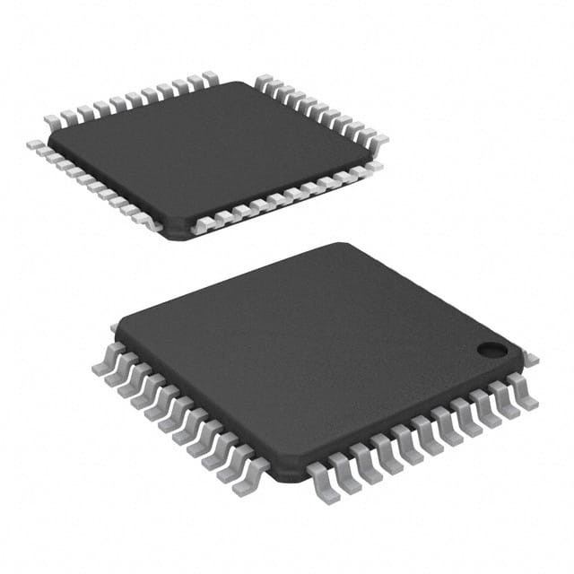
- Part No.:
- CY8C4245AXI-473
- Manufacturer:
- Infineon Technologies
- Category:
- Microcontrollers
- Package:
- 44-LQFP
- Datasheet:
-
 CY8C4245AXI-473.pdf
- Description:
- IC MCU 32BIT 32KB FLASH 44TQFP
- Quantity:
- Payment:

- Shipping:

Inventory:1,154
Please send an inquiry. Send us your inquiry, and we will respond immediately.
Product details
Overview
CY8C4245AXI-473 from Infineon Technologies (formerly Cypress Semiconductor) is a 32-bit Arm® Cortex™-M0 programmable system-on-chip (PSoC® 4200 family) integrating MCU, reconfigurable analog/digital blocks, 12-bit 1-Msps SAR ADC, two opamps with comparator mode, and two SCBs supporting I²C/SPI/UART. It operates from 1.71 V to 5.5 V and supports –40 °C to +105 °C industrial temperature range. Used in capacitive touch HMI, motor control feedback, and low-power sensor nodes.
For engineers reviewing the CY8C4245AXI-473 datasheet, CY8C4245AXI-473 pinout, CY8C4245AXI-473 application, or CY8C4245AXI-473 equivalent, key selection criteria include its 48-MHz CPU with single-cycle multiply, 32 kB flash + 4 kB SRAM, programmable UDB-based digital logic, CapSense Sigma-Delta (CSD) support with >5:1 SNR, and SWD debug interface with four breakpoint comparators.
Technical Context
The device implements a tightly coupled AHB-Lite bus architecture with dedicated SRAM controller, ROM boot loader, and flash accelerator enabling 1-wait-state access at 48 MHz. Its analog subsystem includes CTBm (Capacitive Touch Block) and SAR ADC with channel sequencer and signal averaging - both accessible via DSI (Digital System Interconnect) for synchronized digital control.
Digital programmability centers on four Universal Digital Blocks (UDBs), each containing eight macrocells and a data path, supporting user-defined state machines or Verilog-derived logic. All peripherals-including TCPWM, SCBs, and LCD drivers-are routed through a high-flexibility I/O matrix with programmable drive modes, slew rates, and interrupt-capable GPIOs.
Key Specifications
| Parameter | Value and Actual Design Meaning |
|---|---|
| CPU Core | Arm Cortex-M0, 48 MHz max, single-cycle 32-bit multiply - enables deterministic real-time control and Thumb-2 binary compatibility with higher Cortex-M families. |
| Memory | 32 kB flash (with Read Accelerator), 4 kB SRAM - sufficient for firmware + CapSense tuning tables; SRAM retained in Hibernate mode. |
| Analog ADC | 12-bit SAR, 1 Msps, differential/single-ended, channel sequencer with hardware averaging - supports multi-sensor acquisition without CPU overhead. |
| CapSense | CapSense Sigma-Delta (CSD) engine with SmartSense™ auto-tuning - delivers >5:1 SNR and water-tolerant touch detection on any GPIO. |
| Digital Logic | 4 UDBs (each: 8 macrocells + data path) - enables custom PWM generators, protocol encoders, or glue logic without external components. |
| Communication | 2 SCBs configurable as I²C/SPI/UART - runtime-reconfigurable per peripheral instance, supporting mixed-mode serial interfaces on shared pins. |
| Power Modes | Stop (20 nA), Deep Sleep, Hibernate - GPIO wakeup from Stop mode enables ultra-low-power wake-on-event sensing. |
Pinout & Package
Package: 48-pin TQFP (7 mm × 7 mm, 0.5 mm pitch), RoHS-compliant, moisture sensitivity level 3.
| Pin/Terminal | Circuit Role | Design Meaning |
|---|---|---|
| VDD | Main power supply input | 1.71–5.5 V analog/digital core supply; decoupling required per datasheet layout guidelines. |
| VSS | Ground reference | Common return for analog/digital domains; separate AGND/DGND routing recommended. |
| P0[0]–P0[7] | Programmable GPIO port 0 | Support CapSense, analog input, LCD segment/common, or digital logic; all drive modes configurable. |
| P1[0]–P1[7] | Programmable GPIO port 1 | Includes SWDIO/SWCLK pins (P1[0]/P1[1]); default debug interface, disableable for security. |
| P2[0]–P2[7] | Programmable GPIO port 2 | Supports TCPWM capture/compare outputs and SCB signal routing (e.g., I²C SCL/SDA). |
| XRES | External reset input | Active-low asynchronous reset; internal pull-up enabled; compatible with open-drain reset supervisors. |
| XTAL_IN / XTAL_OUT | Crystal oscillator connection | Supports 1–33 MHz crystal; optional internal IMO (Internal Main Oscillator) bypasses need for external crystal. |
Key Features
| Feature | Design Value |
|---|---|
| CapSense CSD Engine | Hardware-accelerated sigma-delta modulation with >5:1 SNR and automatic SmartSense™ tuning - eliminates manual calibration for production touch panels. |
| Programmable UDB Array | Four independent universal digital blocks with macrocell-level configurability - replaces discrete logic ICs and reduces BOM count in motor control or protocol bridging. |
| SWD Debug Interface | 2-wire Serial Wire Debug with 4 address breakpoints and 2 data watchpoints - enables full on-chip debugging without JTAG pod or emulator. |
| Flash Protection Modes | Open / Protected / Kill - "Kill" mode permanently disables external flash access and debug, preventing reverse engineering or unauthorized reprogramming. |
| Low-Power Wakeup | 20-nA Stop mode with GPIO-triggered wakeup - supports battery-powered devices requiring years of shelf life before activation. |
Applications
| Industrial HMI Panels | Smart Appliance Control |
|---|---|
Use Scenario: Touch-enabled control panel for HVAC, PLC interface, or factory display with glove/water tolerance requirements. IC Role / Device Role / Timing Role: Primary system controller running CapSense firmware and driving segmented LCD display in Deep Sleep mode. Use Value: Single-chip integration of touch sensing, display driver, and communication (I²C to MCU host) eliminates external touch controller and reduces PCB area by ≥30%. | Use Scenario: Washing machine or dishwasher main control board managing motor timing, water level sensing, and user interface. IC Role / Device Role / Timing Role: Real-time motor commutation supervisor using TCPWM blocks with comparator-triggered kill signals for overcurrent protection. Use Value: Hardware-synchronized PWM dead-time insertion and fault response within <100 ns avoids MOSFET shoot-through without software latency. |
| Portable Medical Sensors | IoT Edge Node Controllers |
Use Scenario: Battery-powered pulse oximeter or glucose meter requiring analog front-end precision and ultra-low standby current. IC Role / Device Role / Timing Role: Analog signal conditioner (opamp + SAR ADC) and BLE subsystem coordinator (via UART to companion radio). Use Value: 12-bit ADC with hardware averaging achieves <1 LSB noise floor at 100 ksps; 20-nA Stop mode extends coin-cell life to >5 years. | Use Scenario: Wireless environmental monitor collecting temperature, humidity, and motion data for cloud upload. IC Role / Device Role / Timing Role: Sensor fusion hub aggregating I²C sensor data, performing local thresholding, and waking radio only on event. Use Value: Programmable digital logic (UDBs) offloads sensor polling and event filtering from CPU, reducing active time by 65% versus software-only implementation. |
Equivalent & Alternatives
The following parts are listed as comparable options for similar programmable mixed-signal controller applications.
| Alternative Part | Technical Difference | Application Difference | Selection Advice |
|---|---|---|---|
| CY8C4247AZI-M485 | Same PSoC 4200 family, 44-pin TQFP, 256 kB flash, 32 kB SRAM - larger memory, same peripherals and clock architecture. | Targeted at firmware-rich applications (e.g., OTA updates, complex UI stacks) where CY8C4245AXI-473's 32 kB flash is limiting. | Select when code size exceeds 28 kB or future firmware expansion is required; pin-compatible but different package footprint. |
| STM32L432KC | Arm Cortex-M4, 80 MHz, 256 kB flash, 64 kB SRAM, no integrated CapSense or UDBs - adds FPU and DSP instructions but lacks analog/digital reconfigurability. | Suitable for math-intensive sensor processing but requires external touch controller and logic ICs for CapSense or custom PWM. | Select when floating-point computation dominates and analog/digital flexibility is secondary; not pin- or firmware-compatible. |
Compared with CY8C4245AXI-473, CY8C4247AZI-M485 offers scalable memory while retaining identical analog/digital IP and toolchain compatibility, whereas STM32L432KC trades programmable hardware blocks for higher CPU performance and standard ARM ecosystem support - making it better suited for algorithm-heavy rather than hardware-integration tasks.
Availability
CY8C4245AXI-473 is available at Aetrix Electronics and suitable for industrial HMI, smart appliance control, portable medical sensors, and IoT edge node controllers requiring stable component supply across extended temperature ranges and long product lifecycles.
Supply support for CY8C4245AXI-473 includes scheduled delivery planning, volume procurement assistance, BOM continuity management, traceable sourcing, and lifecycle availability coordination for OEM customers, industrial embedded developers, connected-device designers, and electronics production programs.
Manufacturer
Infineon Technologies is a global semiconductor leader headquartered in Munich, Germany, specializing in power management, automotive MCUs, and secure connectivity solutions.
CY8C4245AXI-473 belongs to the PSoC® 4200 family - designed specifically for cost-sensitive, low-power embedded systems needing hardware-level reconfigurability of analog and digital functions without external components.
FAQ
Does CY8C4245AXI-473 support USB communication?
No. The device does not integrate a USB PHY or USB controller. Communication is limited to the two SCBs supporting I²C, SPI, or UART protocols. For USB connectivity, an external USB-to-UART bridge (e.g., CP2102) or companion MCU with USB capability is required.
Can the SAR ADC perform simultaneous sampling on multiple channels?
No. The single 12-bit SAR ADC supports sequential sampling via hardware channel sequencing and averaging, but lacks dual-sample-and-hold circuitry for true simultaneous acquisition. Multi-channel synchronization is achieved through precise timer-triggered start delays, not concurrent conversion.
Is the CapSense functionality available on all GPIO pins?
Yes. All 36 GPIOs support CapSense CSD operation, including pins shared with analog inputs, LCD segments, or digital peripherals. Pin assignment is fully configurable in PSoC Creator, and mutual-capacitance or self-capacitance topologies can be implemented on any combination of pins.
What debug interfaces are supported, and can they be disabled permanently?
The device supports only Serial Wire Debug (SWD) via P1[0] (SWDIO) and P1[1] (SWCLK). Debug can be disabled in firmware; once set to "Protected" or "Kill" flash protection mode, SWD access is blocked until full flash erase (Protected) or permanently (Kill), enforcing hardware-level security against unauthorized access.
CY8C4245AXI-473 Specifications
- Product attributes
- Attribute value
- Manufacturer:
- Infineon Technologies
- Package/Case:
- 44-LQFP
- Series:
- PSOC™ 4 CY8C42xx
- Packaging:
- Tray
- Product Status:
- Active
- Programmable:
- Not Verified
- Core Processor:
- ARM® Cortex®-M0
- Core Size:
- 32-Bit Single-Core
- Speed:
- 48MHz
- Connectivity:
- I2C, IrDA, LINbus, Microwire, SmartCard, SPI, SSP, UART/USART
- Peripherals:
- Brown-out Detect/Reset, LVD, POR, PWM, WDT
- Number of I/O:
- 36
- Program Memory Size:
- 32KB (32K x 8)
- Program Memory Type:
- FLASH
- EEPROM Size:
- -
- RAM Size:
- 4K x 8
- Voltage - Supply (Vcc/Vdd):
- 1.71V ~ 5.5V
- Data Converters:
- A/D 8x12b SAR; D/A 2xIDAC
- Oscillator Type:
- Internal
- Operating Temperature:
- -40°C ~ 85°C (TA)
- Grade:
- -
- Qualification:
- -
- Mounting Type:
- Surface Mount
- Supplier Device Package:
CY8C4245AXI-473 FAQ
1.How can I place an order for CY8C4245AXI-473 through Aetrix?
Please submit a Request for Quotation (RFQ) for CY8C4245AXI-473 on Aetrix. Our sales agent will provide a competitive quotation and guide you through the order confirmation once you accept the terms.
2.Are the price and stock information for CY8C4245AXI-473 reliable?
The price and inventory of CY8C4245AXI-473 are updated periodically and may fluctuate due to market conditions. Stock and pricing data are typically refreshed every 24 hours. Quotation validity for CY8C4245AXI-473 is usually 5 days.
3.What payment methods are accepted for CY8C4245AXI-473?
We accept Wire Transfer, PayPal, Credit Card, Western Union, MoneyGram, and Escrow for CY8C4245AXI-473 transactions.
Note: Certain payment methods may incur a processing fee.
4.How is shipping managed for CY8C4245AXI-473?
CY8C4245AXI-473 orders can be shipped via leading logistics carriers, including DHL, UPS, FedEx, TNT, or Registered Mail.
Once your CY8C4245AXI-473 order is processed, you will receive an email with the shipment details and tracking number.
Note: Tracking information may take up to 24 hours to appear. Express delivery typically takes 3–5 business days.
5.How can I obtain technical support or documentation for CY8C4245AXI-473?
For technical support, including CY8C4245AXI-473 datasheets, pinout diagrams, or application guidance, please contact our engineering support team. They can provide detailed documentation and assistance for your CY8C4245AXI-473 requirements.
6.How does Aetrix verify that CY8C4245AXI-473 is sourced from the original manufacturer or authorized distributors?
All CY8C4245AXI-473 products on Aetrix are procured from qualified distributors and authorized channels. Our dedicated quality assurance team conducts strict verification, including traceability checks and, if necessary, third-party testing. This ensures that CY8C4245AXI-473 meets industry standards.
7.What is the process for return or replacement of CY8C4245AXI-473?
All CY8C4245AXI-473 units undergo pre-shipment inspection (PSI). If there is an issue with CY8C4245AXI-473, returns or replacements are accepted under the following conditions:
1.Quantity discrepancies, incorrect items, or visible external defects (such as breakage or corrosion), acknowledged by Aetrix.
2.The issue is reported within 90 days of delivery.
3.The CY8C4245AXI-473 part is unused and in its original packaging.
Return procedure for CY8C4245AXI-473:
1.Submit a request within 90 days.
2.Obtain a Return Material Authorization (RMA) from Aetrix.
CY8C4245AXI-473 Tags

-
ATTINY4-TSHR
Microchip Technology
-
ATTINY10-TSHR
Microchip Technology
-
ATTINY10-TS8R
Microchip Technology

-
ATTINY202-SSNR
Microchip Technology
-
ATTINY202-SSFR
Microchip Technology
-
ATTINY402-SSNR
Microchip Technology

-
PIC16F15213T-I/MF
Microchip Technology
-
PIC16F15213-E/MF
Microchip Technology

-
PIC10F200T-I/OT
Microchip Technology
-
ATTINY412-SSNR
Microchip Technology
-
PIC10F202T-I/OT
Microchip Technology

-
ATTINY404-SSNR
Microchip Technology
Tech Hub

18650 battery guide covering lithium-ion cell basics, 3.6V/3.7V voltage, 4.2V charging, mAh and Wh capacity, protected cells, chargers, BMS, series-parallel packs, holders, welding and sourcing checks.…

Hall effect sensor guide covering working principle, linear and digital sensors, Arduino circuits, current sensing, speed detection, automotive applications, A3144 examples, signal filtering and datash…

Product Change Notification guide for electronic components, covering PCN meaning, PCN vs PDN/EOL, common change types, risk levels, form-fit-function review, engineering validation, BOM control, LTB/L…

A practical guide to blend door actuators, covering HVAC function, symptoms, location, AC and heater issues, reset and calibration, replacement cost, electrical diagnosis, compatibility checks, and rep…

Engineering guide to Raspberry Pi alternatives, covering chip-level differences, Orange Pi, ROCK, Jetson, Banana Pi, NanoPi, Compute Module, Pico, GPIO, camera, HAT compatibility, and replacement risks…

Engineering guide to dynamic load response testing for high-current buck converters, covering load step setup, slew rate, Vcore undershoot, overshoot, recovery time, probe location, output capacitors a…

Engineering guide to output capacitor selection for ASIC Vcore rails, covering bulk capacitors, polymer capacitors, MLCC decoupling, DC bias, ESR, ESL, placement, transient response and substitution ri…

Engineering guide to high-current ASIC Vcore rails, covering 12-phase buck architecture, PMBus control, dynamic load testing, output capacitor networks, smart power stage selection, thermal design and …

Voltage regulator guide covering linear, LDO, 7805, Zener, adjustable, buck, VRM and alternator regulators, with design checks, testing methods, troubleshooting and datasheet-based selection.

Amplifier guide covering voltage, current and power amplification, gain, feedback, amplifier classes, audio and RF applications, op-amp circuits, transimpedance amplifiers, datasheet selection and trou…


