
 My Inquiry
 My Account


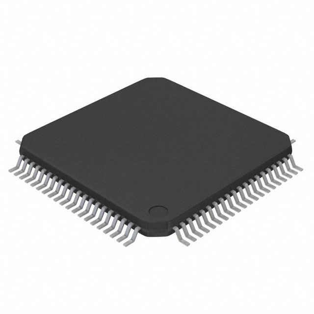
Infineon Technologies CY9AF156MBPMC-G-JNE2
- Part No.:
- CY9AF156MBPMC-G-JNE2
- Manufacturer:
- Infineon Technologies
- Category:
- Microcontrollers
- Package:
- 80-LQFP
- Datasheet:
-
 CY9AF156MBPMC-G-JNE2.pdf
- Description:
- IC MCU 32BIT 544KB FLASH 80LQFP
- Quantity:
- Payment:

- Shipping:

Inventory:3,141
Please send an inquiry. Send us your inquiry, and we will respond immediately.
Product details
Overview
CY9AF156MBPMC-G-JNE2 from Infineon Technologies (formerly Cypress) is a 32-bit Arm® Cortex®-M3 microcontroller with 512 KB dual-bank Flash (496 KB upper + 16 KB lower), 64 KB on-chip SRAM (32 KB SRAM0 + 32 KB SRAM1), and operates up to 40 MHz. It integrates UART/CSIO/I²C serial interfaces, 24-channel 12-bit ADC (2.0 µs conversion), 16-channel base timer, RTC, QPRC, HDMI-CEC, and six low-power modes - deployed in industrial motor control and embedded HMI systems.
For engineers reviewing the CY9AF156MBPMC-G-JNE2 datasheet, CY9AF156MBPMC-G-JNE2 pinout, CY9AF156MBPMC-G-JNE2 application, or CY9AF156MBPMC-G-JNE2 equivalent, key selection criteria include dual-bank Flash for seamless firmware updates, 5 V-tolerant I/O support on selected pins, hardware CRC acceleration (CRC16/CRC32), SWJ-DP debug interface, and deep-standby RTC mode with RAM retention.
Technical Context
This MCU implements a tightly coupled Arm Cortex-M3 r2p1 core with NVIC supporting 48 peripheral interrupts and 16 priority levels, plus a 24-bit SysTick timer for RTOS scheduling. Its memory subsystem features dual-operation Flash enabling concurrent read-erase-write across banks and two independent SRAM blocks (SRAM0 on I/D-code bus, SRAM1 on system bus) for deterministic real-time execution.
The peripheral set includes a 16-channel multi-function serial interface configurable per channel as UART, CSIO, or I²C; an 8-channel DMA controller with 32-bit addressing and burst/block/demand transfer modes; and dedicated motor-control blocks including PWM, PPG, dead-time insertion, and A/D activation compare - all synchronized via shared clock domains and trigger routing.
Key Specifications
| Parameter | Value and Actual Design Meaning |
|---|---|
| CPU Core | Arm Cortex-M3 r2p1, up to 40 MHz - enables deterministic real-time task scheduling with low interrupt latency. |
| Flash Memory | 512 KB dual-bank (496 KB upper + 16 KB lower), 0-wait-state read - supports background firmware update without halting execution. |
| SRAM | 64 KB total (32 KB SRAM0 + 32 KB SRAM1), independently bus-connected - isolates instruction/data access from system peripherals to avoid bus contention. |
| ADC | 24-channel 12-bit SAR, 2.0 µs conversion @ 2.7–3.6 V - meets fast-sampling requirements for motor current sensing and sensor fusion. |
| Low-Power Modes | Six modes including Deep Standby RTC with RAM retention - extends battery life in always-on embedded controllers. |
| Clock Sources | Five sources: 4–48 MHz main oscillator, 32.768 kHz sub-clock, 4 MHz/100 kHz CR oscillators, PLL - enables robust clock supervision and failover. |
| Debug Interface | Serial Wire JTAG Debug Port (SWJ-DP) only - provides full debug visibility without ETM trace, suitable for cost-sensitive production firmware validation. |
Pinout & Package
Package: LQFP-120 (14 mm × 14 mm, 0.4 mm pitch), RoHS-compliant, moisture sensitivity level 3.
| Pin/Terminal | Circuit Role | Design Meaning |
|---|---|---|
| VCC / VSS | Power supply / Ground | Dedicated analog/digital power pins with decoupling requirements specified per section 7.2 of datasheet - ensures stable operation across voltage range (1.65–3.6 V). |
| XTAL / EXTAL | Main crystal oscillator input/output | Connects to 4–48 MHz parallel-resonant crystal - forms primary clock source with PLL multiplication for CPU/peripheral timing. |
| XTAL32 / EXTAL32 | Sub-crystal oscillator input/output | Drives 32.768 kHz watch crystal - supplies RTC and deep-standby clocking with ±20 ppm stability over temperature. |
| MD0 | Boot mode select | Pulled high at reset to enable Flash boot mode - determines initial vector table location and memory mapping configuration. |
| INITX | External reset input | Active-low asynchronous reset pin - allows external supervisory IC or push-button reset independent of internal LVD/CSV events. |
| PA0–PA15, PB0–PB15, etc. | Multi-function GPIO | Up to 103 high-speed I/O pins with port relocate function and per-pin pull-up control - enables flexible PCB layout and peripheral remapping without hardware change. |
Key Features
| Feature | Design Value |
|---|---|
| Dual-bank Flash memory | Enables Over-the-Air (OTA) firmware updates with zero downtime: one bank executes while the other is erased/written. |
| Hardware CRC accelerator | Offloads CCITT CRC16 and IEEE-802.3 CRC32 computation from CPU - reduces integrity check latency in communication stacks and flash verification. |
| Quadrature Position Counter (QPRC) | 16-bit position + 16-bit revolution counters with configurable A/B/Z input edge detection - directly interfaces rotary encoders in motor feedback loops. |
| HDMI-CEC controller | Full protocol stack support including automatic ACK, arbitration loss detection, and header block transmission - enables remote control interoperability in AV equipment. |
| Two watchdog timers | Independent hardware (CR-oscillator clocked) and software watchdogs - provides layered failure recovery: hardware WD covers deep sleep, software WD monitors application logic. |
Applications
| Industrial Motor Control | Smart Home HMI Controller |
|---|---|
Use Scenario: Closed-loop BLDC/PMSM motor drive with current sensing, position feedback, and thermal monitoring. IC Role / Device Role / Timing Role: Main system controller executing FOC algorithm, managing PWM generation with dead-time insertion, triggering ADC sampling on current sense channels, and reading QPRC encoder data. Use Value: Integrated motor-control peripherals reduce external component count; dual-bank Flash enables field-upgradable motion profiles without stopping operation. | Use Scenario: Touch-enabled wall panel controlling lighting, HVAC, and security subsystems via Zigbee/Z-Wave gateways. IC Role / Device Role / Timing Role: Application processor handling UI rendering, sensor polling (temp/humidity), local decision logic, and HDMI-CEC command relay to AV devices. Use Value: RTC with alarm interrupt enables scheduled actions; 5 V-tolerant GPIO simplifies interfacing with legacy home automation buses. |
| Energy Metering Gateway | Factory Automation I/O Module |
Use Scenario: Substation-level energy aggregator collecting data from CT/PT sensors and communicating via RS-485/M-Bus to SCADA. IC Role / Device Role / Timing Role: Data concentrator performing ADC oversampling, CRC-protected frame assembly, and UART-to-M-Bus protocol translation with precise timing. Use Value: Hardware CRC32 accelerates frame integrity checks; 24-channel ADC supports simultaneous voltage/current/temperature acquisition. | Use Scenario: DIN-rail mounted digital I/O expansion unit with isolated inputs/outputs and Modbus RTU over RS-485. IC Role / Device Role / Timing Role: Protocol bridge converting Modbus register reads/writes into GPIO state changes and interrupt-driven input capture for pulse counting. Use Value: External bus interface supports optional NOR Flash for field-upgradable firmware; 16-channel base timer handles high-frequency input capture up to 1 MHz. |
Equivalent & Alternatives
The following parts are listed as comparable options for similar 32-bit Arm Cortex-M3 microcontroller applications.
| Alternative Part | Technical Difference | Application Difference | Selection Advice |
|---|---|---|---|
| STM32F103VCT6 | 72 MHz Cortex-M3, 256 KB Flash, 48 KB SRAM, no dual-bank Flash or QPRC - lacks encoder counter and hardware CRC. | Targeted at general-purpose control where encoder interface and OTA update are not required. | Select when higher CPU speed is prioritized over motor-specific peripherals and firmware update safety. |
| RA4M1 (R7FA4M1AB3CFM) | 48 MHz Cortex-M4F, 256 KB Flash, 32 KB SRAM, includes ELC event linker but no dual-bank Flash or HDMI-CEC. | Optimized for low-power IoT edge nodes with DSP extensions, not industrial motor control or AV integration. | Prefer when floating-point math or secure boot is needed, and HDMI-CEC/QPRC are unnecessary. |
Compared with STM32F103VCT6 and RA4M1, CY9AF156MBPMC-G-JNE2 uniquely combines dual-bank Flash for safe firmware updates, integrated QPRC for direct encoder interfacing, and HDMI-CEC for consumer electronics control - making it optimal for cost-sensitive, feature-dense embedded controllers requiring field maintainability and AV ecosystem compatibility.
Availability
CY9AF156MBPMC-G-JNE2 is available at Aetrix Electronics and suitable for industrial motor control, smart home HMI, energy metering gateways, and factory automation I/O modules requiring stable component supply across long product lifecycles.
Supply support for CY9AF156MBPMC-G-JNE2 includes scheduled delivery planning, volume procurement assistance, BOM continuity management, traceable sourcing, and lifecycle availability coordination for OEM customers, industrial embedded developers, connected-device designers, and electronics production programs.
Manufacturer
Infineon Technologies is a global semiconductor leader headquartered in Munich, Germany, specializing in power management, automotive MCUs, and security solutions.
This device belongs to the FM3 family of 32-bit Arm Cortex-M3 microcontrollers, designed specifically for cost-optimized, low-power embedded control applications in industrial automation, motor drives, and consumer electronics with integrated analog and communication peripherals.
FAQ
What is the maximum operating frequency and supported voltage range?
The CY9AF156MBPMC-G-JNE2 operates at up to 40 MHz and supports a wide supply voltage range of 1.65 V to 3.6 V. This range accommodates both battery-powered and industrial 3.3 V systems while maintaining full peripheral functionality, including ADC accuracy and Flash programming voltage tolerance.
Does this MCU support in-system programming and secure code protection?
Yes, it supports in-system programming via SWJ-DP interface and includes Flash security functions such as code protection lock bits and read-out protection. These features prevent unauthorized access to firmware during development, production, and field deployment - critical for IP-sensitive applications like proprietary motor algorithms.
How many I/O pins are 5 V tolerant, and where is this specified?
Selected GPIO pins (including PA0–PA7, PB0–PB7, PC0–PC7, PD0–PD7, and specific alternate-function pins) are 5 V tolerant. This is confirmed in the "List of Pin Function and I/O Circuit Type" section (pages 39–64) of the official datasheet (002-05646 Rev. *F), which maps each pin's electrical type and voltage rating.
Is external memory expansion supported, and what interfaces are available?
Yes, it supports external memory expansion via an 8-chip-select External Bus Interface (EBI) with 8-/16-bit data width and up to 25-bit addressing (256 MB address space). It interfaces with SRAM, NOR Flash, and NAND Flash devices, and supports address/data multiplexing and external RDY handshake for timing flexibility.
CY9AF156MBPMC-G-JNE2 Specifications
- Product attributes
- Attribute value
- Manufacturer:
- Infineon Technologies
- Package/Case:
- 80-LQFP
- Series:
- FM3 MB9A150RB
- Packaging:
- Tray
- Product Status:
- Active
- Programmable:
- Not Verified
- Core Processor:
- ARM® Cortex®-M3
- Core Size:
- 32-Bit Single-Core
- Speed:
- 40MHz
- Connectivity:
- CSIO, EBI/EMI, I2C, SPI, UART/USART
- Peripherals:
- DMA, LVD, POR, PWM, WDT
- Number of I/O:
- 66
- Program Memory Size:
- 544KB (544K x 8)
- Program Memory Type:
- FLASH
- EEPROM Size:
- -
- RAM Size:
- 64K x 8
- Voltage - Supply (Vcc/Vdd):
- 1.65V ~ 3.6V
- Data Converters:
- A/D 17x12b
- Oscillator Type:
- Internal
- Operating Temperature:
- -40°C ~ 85°C (TA)
- Grade:
- -
- Qualification:
- -
- Mounting Type:
- Surface Mount
- Supplier Device Package:
CY9AF156MBPMC-G-JNE2 FAQ
1.How can I place an order for CY9AF156MBPMC-G-JNE2 through Aetrix?
Please submit a Request for Quotation (RFQ) for CY9AF156MBPMC-G-JNE2 on Aetrix. Our sales agent will provide a competitive quotation and guide you through the order confirmation once you accept the terms.
2.Are the price and stock information for CY9AF156MBPMC-G-JNE2 reliable?
The price and inventory of CY9AF156MBPMC-G-JNE2 are updated periodically and may fluctuate due to market conditions. Stock and pricing data are typically refreshed every 24 hours. Quotation validity for CY9AF156MBPMC-G-JNE2 is usually 5 days.
3.What payment methods are accepted for CY9AF156MBPMC-G-JNE2?
We accept Wire Transfer, PayPal, Credit Card, Western Union, MoneyGram, and Escrow for CY9AF156MBPMC-G-JNE2 transactions.
Note: Certain payment methods may incur a processing fee.
4.How is shipping managed for CY9AF156MBPMC-G-JNE2?
CY9AF156MBPMC-G-JNE2 orders can be shipped via leading logistics carriers, including DHL, UPS, FedEx, TNT, or Registered Mail.
Once your CY9AF156MBPMC-G-JNE2 order is processed, you will receive an email with the shipment details and tracking number.
Note: Tracking information may take up to 24 hours to appear. Express delivery typically takes 3–5 business days.
5.How can I obtain technical support or documentation for CY9AF156MBPMC-G-JNE2?
For technical support, including CY9AF156MBPMC-G-JNE2 datasheets, pinout diagrams, or application guidance, please contact our engineering support team. They can provide detailed documentation and assistance for your CY9AF156MBPMC-G-JNE2 requirements.
6.How does Aetrix verify that CY9AF156MBPMC-G-JNE2 is sourced from the original manufacturer or authorized distributors?
All CY9AF156MBPMC-G-JNE2 products on Aetrix are procured from qualified distributors and authorized channels. Our dedicated quality assurance team conducts strict verification, including traceability checks and, if necessary, third-party testing. This ensures that CY9AF156MBPMC-G-JNE2 meets industry standards.
7.What is the process for return or replacement of CY9AF156MBPMC-G-JNE2?
All CY9AF156MBPMC-G-JNE2 units undergo pre-shipment inspection (PSI). If there is an issue with CY9AF156MBPMC-G-JNE2, returns or replacements are accepted under the following conditions:
1.Quantity discrepancies, incorrect items, or visible external defects (such as breakage or corrosion), acknowledged by Aetrix.
2.The issue is reported within 90 days of delivery.
3.The CY9AF156MBPMC-G-JNE2 part is unused and in its original packaging.
Return procedure for CY9AF156MBPMC-G-JNE2:
1.Submit a request within 90 days.
2.Obtain a Return Material Authorization (RMA) from Aetrix.
CY9AF156MBPMC-G-JNE2 Tags

-
ATTINY4-TSHR
Microchip Technology
-
ATTINY10-TSHR
Microchip Technology
-
ATTINY10-TS8R
Microchip Technology

-
ATTINY202-SSNR
Microchip Technology
-
ATTINY202-SSFR
Microchip Technology
-
ATTINY402-SSNR
Microchip Technology

-
PIC16F15213T-I/MF
Microchip Technology
-
PIC16F15213-E/MF
Microchip Technology

-
PIC10F200T-I/OT
Microchip Technology
-
ATTINY412-SSNR
Microchip Technology
-
PIC10F202T-I/OT
Microchip Technology

-
ATTINY404-SSNR
Microchip Technology
Tech Hub

Guide to electronic component obsolescence covering EOL risk, PCN/PDN notices, last-time buy planning, replacement options, form-fit-function validation, counterfeit risk and BOM lifecycle management.

18650 battery guide covering lithium-ion cell basics, 3.6V/3.7V voltage, 4.2V charging, mAh and Wh capacity, protected cells, chargers, BMS, series-parallel packs, holders, welding and sourcing checks.…

Hall effect sensor guide covering working principle, linear and digital sensors, Arduino circuits, current sensing, speed detection, automotive applications, A3144 examples, signal filtering and datash…

Product Change Notification guide for electronic components, covering PCN meaning, PCN vs PDN/EOL, common change types, risk levels, form-fit-function review, engineering validation, BOM control, LTB/L…

A practical guide to blend door actuators, covering HVAC function, symptoms, location, AC and heater issues, reset and calibration, replacement cost, electrical diagnosis, compatibility checks, and rep…

Engineering guide to Raspberry Pi alternatives, covering chip-level differences, Orange Pi, ROCK, Jetson, Banana Pi, NanoPi, Compute Module, Pico, GPIO, camera, HAT compatibility, and replacement risks…

Engineering guide to dynamic load response testing for high-current buck converters, covering load step setup, slew rate, Vcore undershoot, overshoot, recovery time, probe location, output capacitors a…

Engineering guide to output capacitor selection for ASIC Vcore rails, covering bulk capacitors, polymer capacitors, MLCC decoupling, DC bias, ESR, ESL, placement, transient response and substitution ri…

Engineering guide to high-current ASIC Vcore rails, covering 12-phase buck architecture, PMBus control, dynamic load testing, output capacitor networks, smart power stage selection, thermal design and …

Voltage regulator guide covering linear, LDO, 7805, Zener, adjustable, buck, VRM and alternator regulators, with design checks, testing methods, troubleshooting and datasheet-based selection.


