
 My Inquiry
 My Account


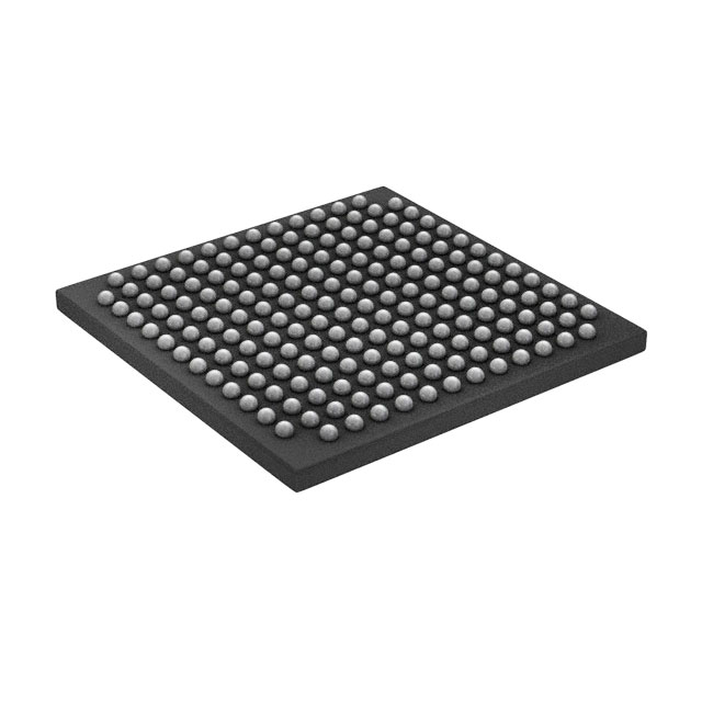
Infineon Technologies CY9BF528TABGL-GK7E1
- Part No.:
- CY9BF528TABGL-GK7E1
- Manufacturer:
- Infineon Technologies
- Category:
- Microcontrollers
- Package:
- 192-LFBGA
- Datasheet:
-
 CY9BF528TABGL-GK7E1.pdf
- Description:
- IC MCU 32B 1.0625MB FLSH 192FBGA
- Quantity:
- Payment:

- Shipping:

Inventory:3,994
Please send an inquiry. Send us your inquiry, and we will respond immediately.
Product details
Overview
CY9BF528TABGL-GK7E1 from Infineon Technologies (formerly Cypress) is a 32-bit Arm® Cortex®-M3 microcontroller with dual-bank flash (1008 KB + 512 KB), 192 KB SRAM, USB 2.0 Full-Speed Device/Host, CAN 2.0A/B, and 24-channel 12-bit ADC. It operates up to 60 MHz, supports six low-power modes, and targets embedded motor control and industrial automation systems requiring integrated timing, communication, and analog interfaces.
For engineers reviewing the CY9BF528TABGL-GK7E1 datasheet, CY9BF528TABGL-GK7E1 pinout, CY9BF528TABGL-GK7E1 application, or CY9BF528TABGL-GK7E1 equivalent, this device offers verified USB/CAN coexistence, hardware CRC acceleration (CCITT CRC16 & IEEE-802.3 CRC32), dual-timer-based motor control waveforms, and 5V-tolerant GPIOs on a 176-pin LQFP package - critical for real-time I/O consolidation in space-constrained designs.
Technical Context
The CY9BF528TABGL-GK7E1 implements a deterministic Arm Cortex-M3 r2p1 core with NVIC supporting 48 peripheral interrupts and 16 priority levels, coupled with dual-bus SRAM architecture (SRAM0 on I/D-code bus, SRAM1 on system bus) enabling concurrent CPU and DMA access. Its clock system integrates five sources including main PLL, sub-clock (32.768 kHz), and dual CR oscillators, with Clock Supervisor (CSV) monitoring external clock integrity via built-in reference clocks.
Peripheral integration includes a multi-function serial interface supporting UART/CSIO/LIN/I²C across 16 channels, two independent 12-bit ADC units with 1.0 µs conversion time and FIFO-based scanning, and a dedicated QPRC block with configurable AIN/BIN/ZIN edge detection for encoder position tracking - all synchronized to a shared APB/AHB bus matrix with external bus interface supporting 256 MB address space.
Key Specifications
| Parameter | Value and Actual Design Meaning |
|---|---|
| CPU Core | Arm Cortex-M3 r2p1, 60 MHz max - enables deterministic real-time task scheduling with 24-bit SysTick timer for OS kernel support. |
| Flash Memory | 1008 KB ROM0 + 512 KB ROM1 + 16 KB lower bank ROM0 - supports dual-operation firmware updates without halting execution. |
| SRAM | 96 KB SRAM0 (I/D bus) + 96 KB SRAM1 (system bus) - allows simultaneous instruction fetch and DMA data transfer without bus contention. |
| ADC | 2 × 12-bit SAR ADC, 1.0 µs conversion @ 2.7–5.5 V - delivers high-speed sensor sampling for closed-loop motor control with scan-mode FIFO buffering. |
| USB Interface | Full-Speed Device/Host with built-in PLL - eliminates external crystal requirement for USB clock generation and supports automatic device attach/detach detection. |
| CAN Interface | CAN 2.0A/B compliant, 1 Mbps max bit rate, 32 message buffers - enables robust automotive-grade communication with hardware message filtering and prioritization. |
| Low-Power Modes | SLEEP, TIMER, RTC, STOP, Deep standby RTC/STOP - provides selectable RAM retention and wake-up sources including QPRC, RTC alarm, and external interrupts. |
Pinout & Package
This device is housed in a 176-pin LQFP package (24 × 24 mm, 0.5 mm pitch) with exposed thermal pad, rated for industrial temperature range (–40°C to +85°C) and qualified per AEC-Q100 Grade 2 for automotive applications.
| Pin/Terminal | Circuit Role | Design Meaning |
|---|---|---|
| VCC / VSS | Power supply / Ground | Dedicated power domains for core (2.7–5.5 V), USB (3.0–3.6 V), and analog (separate AVCC/AVSS) ensure noise isolation for mixed-signal operation. |
| XTAL / EXTAL | Main clock oscillator input/output | Supports 4–48 MHz crystal or external clock source; required for PLL and USB clock derivation. |
| OSC32K / OSC32KOUT | Sub-clock oscillator input/output | Connects 32.768 kHz crystal for RTC and low-power wake-up timing with CSV supervision. |
| USB_DP / USB_DM | USB 2.0 Full-Speed differential pair | Integrated transceivers with internal termination; require only 27 Ω series resistors and ESD protection per USB spec. |
| CAN_TX / CAN_RX | CAN controller physical layer interface | CMOS-level signals requiring external CAN transceiver (e.g., TJA1042) for bus coupling and fault protection. |
| PA0–PA15, PB0–PB15, etc. | Multi-function GPIO | 154 total high-speed I/O pins with port relocation, 5V tolerance on selected pins, and individual pull-up control for flexible board routing. |
Key Features
| Feature | Design Value |
|---|---|
| Dual-bank Flash with zero-wait read | Enables background firmware update while executing from alternate bank - critical for fail-safe field upgrades in industrial controllers. |
| Hardware CRC accelerator | Offloads CCITT CRC16 and IEEE-802.3 CRC32 computation from CPU, reducing integrity check latency by >90% for CAN/USB packet validation. |
| Quadrature Position Counter (QPRC) | Configurable edge detection on AIN/BIN/ZIN with 16-bit position/revolution counters - eliminates need for external encoder interface IC in motor feedback loops. |
| Multi-function serial interface (16 ch) | Per-channel mode selection (UART/CSIO/LIN/I²C) with double-buffered TX/RX and dedicated baud rate generators - simplifies protocol mixing on shared PCB traces. |
| Real-time clock with leap-year support | Full BCD calendar (Year/Month/Day/Hour/Minute/Second/Weekday) with auto-leap-year correction and alarm interrupt down to minute granularity. |
Applications
| Industrial Motor Control | Automotive Body Electronics |
|---|---|
Use Scenario: Closed-loop BLDC/PMSM motor drive with hall-effect or encoder feedback in HVAC blowers or pump systems. IC Role / Device Role / Timing Role: Real-time PWM waveform generation with dead-time insertion, ADC-triggered current sensing, and QPRC-based rotor position tracking. Use Value: Integrated motor control peripherals reduce external component count by ≥30% versus discrete MCU + gate driver + encoder IC solutions. | Use Scenario: Door module controlling window lift, mirror adjustment, and seat position memory in passenger vehicles. IC Role / Device Role / Timing Role: LIN slave node for body control network communication, with local PWM dimming for LED indicators and ADC monitoring of switch inputs. Use Value: Single-chip LIN/UART/I²C support enables unified firmware across multiple vehicle variants, cutting qualification effort by one platform cycle. |
| Smart Energy Metering | Factory Automation I/O Hub |
Use Scenario: DIN-rail mounted electricity meter with tariff switching, tamper detection, and PLC/GPRS backhaul interface. IC Role / Device Role / Timing Role: High-accuracy 12-bit ADC sampling voltage/current transformers, RTC timestamping of energy events, and USB host for field calibration tools. Use Value: Dual-bank flash allows secure over-the-air firmware updates without meter downtime - meeting IEC 62056-21 compliance requirements. | Use Scenario: Modular I/O base unit aggregating digital inputs, analog sensors, and relay outputs for PLC-connected machinery. IC Role / Device Role / Timing Role: Multi-channel UART/CSIO bridging fieldbus protocols (Modbus RTU, CANopen), with DMA-driven data buffering and CRC-protected frame handling. Use Value: Hardware CRC32 acceleration ensures <10 µs frame validation latency - meeting <1 ms cycle time requirements for safety-rated motion control networks. |
Equivalent & Alternatives
The following parts are listed as comparable options for similar microcontroller applications.
| Alternative Part | Technical Difference | Application Difference | Selection Advice |
|---|---|---|---|
| STM32F407VGT6 | ARM Cortex-M4F core, FPU, 1 MB flash, 192 KB RAM, no integrated CAN transceiver support | Lacks native LIN and HDMI-CEC; requires external transceivers for CAN and external CEC PHY | Select when floating-point math or DSP extensions are required; verify external component cost impact on BOM. |
| RA6M4NGB20FBC0 | ARM Cortex-M4 core, 1 MB flash, 384 KB RAM, 64-pin LQFP, no USB host or QPRC | Smaller package and memory footprint; lacks quadrature encoder counter and USB host capability | Choose for compact designs where USB host and precise motor position feedback are not needed. |
Compared with STM32F407VGT6 and RA6M4NGB20FBC0, CY9BF528TABGL-GK7E1 uniquely combines USB host/device, CAN, LIN, QPRC, and HDMI-CEC in a single 176-pin LQFP - eliminating up to four external ICs in multi-protocol industrial gateways.
Availability
CY9BF528TABGL-GK7E1 is available at Aetrix Electronics and suitable for industrial motor control, automotive body electronics, smart energy metering, and factory automation I/O hubs requiring stable component supply, long lifecycle support, and AEC-Q100 Grade 2 qualification.
Supply support for CY9BF528TABGL-GK7E1 includes scheduled delivery planning, volume procurement assistance, BOM continuity management, traceable sourcing, and lifecycle availability coordination for OEM customers, industrial embedded developers, connected-device designers, and electronics production programs.
Manufacturer
Infineon Technologies is a global semiconductor leader headquartered in Munich, Germany, specializing in power management, automotive MCUs, and security solutions with over 50 years of industrial reliability heritage.
The CY9BF528TABGL-GK7E1 belongs to the FM3 family of 32-bit Arm Cortex-M3 microcontrollers, designed specifically for cost-sensitive, low-power embedded control applications demanding rich analog/mixed-signal integration and multi-protocol communication in industrial and automotive environments.
FAQ
What is the maximum operating frequency and supported voltage range for CY9BF528TABGL-GK7E1?
The CY9BF528TABGL-GK7E1 operates at up to 60 MHz and supports a wide VCC supply range of 2.7 V to 5.5 V. USB functionality requires USBVCC between 3.0 V and 3.6 V when active, while GPIO operation remains valid across the full 2.7–5.5 V range. This flexibility enables direct interfacing with both 3.3 V and 5 V legacy peripherals without level-shifting.
Does CY9BF528TABGL-GK7E1 include hardware debug support, and what interface is used?
Yes, it features Serial Wire JTAG Debug Port (SWJ-DP) compliant with ARM CoreSight standards, supporting full breakpoint, watchpoint, and real-time trace via Embedded Trace Macrocell (ETM). No external debug adapter is required beyond standard SWD-capable programmers like Segger J-Link or ST-Link v2.1, enabling seamless integration into CI/CD toolchains.
How does the dual-bank flash architecture enable firmware updates without system interruption?
The dual-bank flash (ROM0 + ROM1) allows one bank to execute code while the other is erased and reprogrammed. Bootloader logic can validate new firmware in the inactive bank before remapping the vector table and initiating a warm reset - achieving zero-downtime field updates essential for unattended industrial equipment and smart grid infrastructure.
Can CY9BF528TABGL-GK7E1 operate in deep sleep modes while maintaining RTC and RAM content?
Yes, in Deep standby RTC mode, the device retains RTC operation and optionally preserves SRAM contents using backup power (VBAT), drawing only ~1.2 µA typical. The RTC continues counting with leap-year correction and can generate wake-up interrupts on date/time match - ideal for battery-backed data loggers and remote sensors with multi-year deployment cycles.
CY9BF528TABGL-GK7E1 Specifications
- Product attributes
- Attribute value
- Manufacturer:
- Infineon Technologies
- Package/Case:
- 192-LFBGA
- Series:
- FM3 MB9B520T
- Packaging:
- Tray
- Product Status:
- Active
- Programmable:
- Not Verified
- Core Processor:
- ARM® Cortex®-M3
- Core Size:
- 32-Bit Single-Core
- Speed:
- 60MHz
- Connectivity:
- CANbus, CSIO, EBI/EMI, I2C, LINbus, UART/USART, USB
- Peripherals:
- DMA, LVD, POR, PWM, WDT
- Number of I/O:
- 154
- Program Memory Size:
- 1.0625MB (1.0625M x 8)
- Program Memory Type:
- FLASH
- EEPROM Size:
- -
- RAM Size:
- 160K x 8
- Voltage - Supply (Vcc/Vdd):
- 2.7V ~ 5.5V
- Data Converters:
- A/D 24x12b; D/A 2x10b
- Oscillator Type:
- Internal
- Operating Temperature:
- -40°C ~ 105°C (TA)
- Grade:
- -
- Qualification:
- -
- Mounting Type:
- Surface Mount
- Supplier Device Package:
CY9BF528TABGL-GK7E1 FAQ
1.How can I place an order for CY9BF528TABGL-GK7E1 through Aetrix?
Please submit a Request for Quotation (RFQ) for CY9BF528TABGL-GK7E1 on Aetrix. Our sales agent will provide a competitive quotation and guide you through the order confirmation once you accept the terms.
2.Are the price and stock information for CY9BF528TABGL-GK7E1 reliable?
The price and inventory of CY9BF528TABGL-GK7E1 are updated periodically and may fluctuate due to market conditions. Stock and pricing data are typically refreshed every 24 hours. Quotation validity for CY9BF528TABGL-GK7E1 is usually 5 days.
3.What payment methods are accepted for CY9BF528TABGL-GK7E1?
We accept Wire Transfer, PayPal, Credit Card, Western Union, MoneyGram, and Escrow for CY9BF528TABGL-GK7E1 transactions.
Note: Certain payment methods may incur a processing fee.
4.How is shipping managed for CY9BF528TABGL-GK7E1?
CY9BF528TABGL-GK7E1 orders can be shipped via leading logistics carriers, including DHL, UPS, FedEx, TNT, or Registered Mail.
Once your CY9BF528TABGL-GK7E1 order is processed, you will receive an email with the shipment details and tracking number.
Note: Tracking information may take up to 24 hours to appear. Express delivery typically takes 3–5 business days.
5.How can I obtain technical support or documentation for CY9BF528TABGL-GK7E1?
For technical support, including CY9BF528TABGL-GK7E1 datasheets, pinout diagrams, or application guidance, please contact our engineering support team. They can provide detailed documentation and assistance for your CY9BF528TABGL-GK7E1 requirements.
6.How does Aetrix verify that CY9BF528TABGL-GK7E1 is sourced from the original manufacturer or authorized distributors?
All CY9BF528TABGL-GK7E1 products on Aetrix are procured from qualified distributors and authorized channels. Our dedicated quality assurance team conducts strict verification, including traceability checks and, if necessary, third-party testing. This ensures that CY9BF528TABGL-GK7E1 meets industry standards.
7.What is the process for return or replacement of CY9BF528TABGL-GK7E1?
All CY9BF528TABGL-GK7E1 units undergo pre-shipment inspection (PSI). If there is an issue with CY9BF528TABGL-GK7E1, returns or replacements are accepted under the following conditions:
1.Quantity discrepancies, incorrect items, or visible external defects (such as breakage or corrosion), acknowledged by Aetrix.
2.The issue is reported within 90 days of delivery.
3.The CY9BF528TABGL-GK7E1 part is unused and in its original packaging.
Return procedure for CY9BF528TABGL-GK7E1:
1.Submit a request within 90 days.
2.Obtain a Return Material Authorization (RMA) from Aetrix.
CY9BF528TABGL-GK7E1 Tags

-
ATTINY4-TSHR
Microchip Technology
-
ATTINY10-TSHR
Microchip Technology
-
ATTINY10-TS8R
Microchip Technology

-
ATTINY202-SSNR
Microchip Technology
-
ATTINY202-SSFR
Microchip Technology
-
ATTINY402-SSNR
Microchip Technology

-
PIC16F15213T-I/MF
Microchip Technology
-
PIC16F15213-E/MF
Microchip Technology

-
PIC10F200T-I/OT
Microchip Technology
-
ATTINY412-SSNR
Microchip Technology
-
PIC10F202T-I/OT
Microchip Technology

-
ATTINY404-SSNR
Microchip Technology
Tech Hub

Guide to electronic component obsolescence covering EOL risk, PCN/PDN notices, last-time buy planning, replacement options, form-fit-function validation, counterfeit risk and BOM lifecycle management.

18650 battery guide covering lithium-ion cell basics, 3.6V/3.7V voltage, 4.2V charging, mAh and Wh capacity, protected cells, chargers, BMS, series-parallel packs, holders, welding and sourcing checks.…

Hall effect sensor guide covering working principle, linear and digital sensors, Arduino circuits, current sensing, speed detection, automotive applications, A3144 examples, signal filtering and datash…

Product Change Notification guide for electronic components, covering PCN meaning, PCN vs PDN/EOL, common change types, risk levels, form-fit-function review, engineering validation, BOM control, LTB/L…

A practical guide to blend door actuators, covering HVAC function, symptoms, location, AC and heater issues, reset and calibration, replacement cost, electrical diagnosis, compatibility checks, and rep…

Engineering guide to Raspberry Pi alternatives, covering chip-level differences, Orange Pi, ROCK, Jetson, Banana Pi, NanoPi, Compute Module, Pico, GPIO, camera, HAT compatibility, and replacement risks…

Engineering guide to dynamic load response testing for high-current buck converters, covering load step setup, slew rate, Vcore undershoot, overshoot, recovery time, probe location, output capacitors a…

Engineering guide to output capacitor selection for ASIC Vcore rails, covering bulk capacitors, polymer capacitors, MLCC decoupling, DC bias, ESR, ESL, placement, transient response and substitution ri…

Engineering guide to high-current ASIC Vcore rails, covering 12-phase buck architecture, PMBus control, dynamic load testing, output capacitor networks, smart power stage selection, thermal design and …

Voltage regulator guide covering linear, LDO, 7805, Zener, adjustable, buck, VRM and alternator regulators, with design checks, testing methods, troubleshooting and datasheet-based selection.


