
 My Inquiry
 My Account


Analog Devices Inc./Maxim Integrated DS3065WP-100IND+
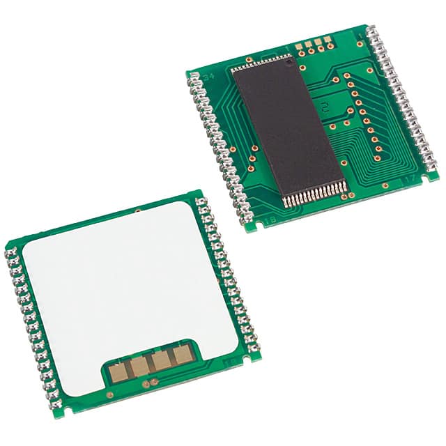
- Part No.:
- DS3065WP-100IND+
- Manufacturer:
- Analog Devices Inc./Maxim Integrated
- Category:
- Memory
- Package:
- 34-PowerCap™ Module
- Datasheet:
-
 DS3065WP-100IND+.pdf
- Description:
- IC NVSRAM 8MBIT PAR 34PWRCAP
- Quantity:
- Payment:

- Shipping:

Inventory:1,139
Please send an inquiry. Send us your inquiry, and we will respond immediately.
Product details
Overview
DS3065WP-100IND+ from Maxim Integrated is a 3.3V, 8Mb (1024k × 8) nonvolatile SRAM with integrated real-time clock (RTC), designed for data retention and timekeeping in power-loss scenarios. It combines static RAM, NV controller, and RTC on a single 34-pin PowerCap module, backed by a DS9034I-PCX+ lithium battery cap. Used in RAID systems, industrial PLCs, and network routers where persistent memory and accurate time stamping are critical.
For engineers reviewing the DS3065WP-100IND+ datasheet, DS3065WP-100IND+ pinout, DS3065WP-100IND+ application, or DS3065WP-100IND+ equivalent, key selection criteria include its 100ns access time, unconditional VCC-fail write protection, battery-backed RTC alarm functionality, extended industrial temperature range (−40°C to +85°C), and direct 3.3V microprocessor interface compatibility.
Technical Context
The DS3065WP-100IND+ integrates three functional blocks: a 1024k × 8 SRAM array, a real-time clock with century/year/month/date/hour/minute/second BCD registers and alarm capability, and a battery-switching controller that automatically engages the DS9034I-PCX+ lithium cell when VCC drops below 2.8V. Its dual-mode addressing-20-bit A0–A19 for SRAM, 4-bit A0–A3 for RTC-enables independent access via CE/CS/WE/OE control signals.
It implements double-buffered RTC registers with read/write halt bits (R/W), oscillator start/stop (OSC), battery-low flag (BLF), and alarm mask bits (AM4–AM1) supporting second-to-monthly alarm intervals. Power-down timing includes tPD = 1.5μs VCC-fail detection and tREC = 125ms recovery before normal operation resumes after VCC restoration.
Key Specifications
| Parameter | Value and Actual Design Meaning |
|---|---|
| Memory Density | 8Mb (1024k × 8 bits) - supports full byte-wide data storage without external multiplexing |
| Access Time | 100ns - enables direct interfacing with 10MHz microprocessors without wait states |
| Supply Voltage | 3.3V ±0.3V - compatible with standard 3.3V logic families and LDO regulators |
| Operating Temperature | −40°C to +85°C - qualified for industrial embedded environments including factory automation and telecom infrastructure |
| Data Retention | 10 years on battery - guaranteed minimum retention under convection reflow + new DS9034I-PCX+ attachment |
| RTC Accuracy | ±1.53 min/month (35ppm) at +25°C - factory-trimmed; no field calibration required |
| Write Protection Threshold | VTP = 2.8V to 3.0V - unconditionally locks SRAM and RTC registers during brownout conditions |
Pinout & Package
DS3065WP-100IND+ uses a surface-mount 34-pin PowerCap module requiring post-assembly attachment of the DS9034I-PCX+ battery cap. The package integrates SRAM, RTC, and battery-switching circuitry on a single substrate with UL recognition (E99151).
| Pin/Terminal | Circuit Role | Design Meaning |
|---|---|---|
| A0–A19 | Address Inputs | 20-bit address bus: A0–A14, A15–A19, A17–A18 used for SRAM; A0–A3 only for RTC register access |
| DQ0–DQ7 | Data I/O Lines | Bi-directional 8-bit data bus shared between SRAM and RTC; high-impedance when CE/CS inactive |
| CE | SRAM Chip Enable | Active-low enable for SRAM read/write; must be low with WE low for SRAM writes |
| CS | RTC Chip Select | Active-low enable for RTC register access; used with WE for RTC writes |
| WE | Write Enable | Active-low universal write strobe; controls write initiation for both SRAM and RTC blocks |
| OE | Output Enable | Active-low output driver control; determines data validity timing (tOE = 50ns, tOEC = 60ns) |
| VCC | Supply Input | 3.3V main power; monitored continuously for fail-detect (VTP threshold) and automatic battery switchover |
| GND | Ground Reference | Common return path for SRAM, RTC, and power-switching circuitry; two dedicated pins (pins 17 and 21) |
| BAT | Battery Terminal | Connection point for DS9034I-PCX+ lithium cell; isolated until VCC falls below VSW (~2.5V) |
| X1/X2 | Crystal Oscillator | 32.768kHz crystal connections for RTC timing; internal load capacitance optimized for standard tuning forks |
Key Features
| Feature | Design Value |
|---|---|
| Integrated RTC with Alarm | Full BCD calendar (century, year, month, date, day, hour, minute, second) plus programmable alarm with AM[4:1] mask bits for second-to-monthly triggers |
| Unconditional Write Protection | Automatic hardware lock of SRAM and RTC registers when VCC drops below 2.8V - no firmware dependency or timing window risk |
| Battery-Swapped Power Path | Dual-supply architecture seamlessly transitions between VCC and DS9034I-PCX+ lithium cell within 1.5μs of VCC failure detection |
| Double-Buffered RTC Registers | Separate internal/external register sets allow atomic reads/writes without time skew; R/W bits enable safe update sequences |
| UL Recognition & RoHS Compliance | Underwriters Laboratories recognized (E99151); "+" suffix indicates lead-free, halogen-free, RoHS-compliant packaging |
Applications
| RAID Systems & Servers | Industrial PLCs |
|---|---|
Use Scenario: Maintaining cache metadata and system timestamps across unexpected AC power loss in enterprise storage arrays. IC Role / Device Role / Timing Role: Nonvolatile SRAM stores configuration and journaling data; RTC provides precise power-loss event time stamps. Use Value: Eliminates need for supercapacitors or backup power supplies while ensuring deterministic 10-year data retention and sub-minute time accuracy. |
Use Scenario: Preserving ladder logic state and operational logs during factory floor brownouts or maintenance shutdowns. IC Role / Device Role / Timing Role: Acts as unified memory + clock source for deterministic scan-cycle logging and scheduled task triggering. Use Value: Enables seamless runtime continuity without external NV memory or discrete RTC ICs, reducing BOM count and PCB area. |
| POS Terminals | Routers & Switches |
Use Scenario: Securing transaction records and audit trails during brief utility interruptions in retail payment systems. IC Role / Device Role / Timing Role: Stores encrypted sales receipts and maintains synchronized time for PCI-DSS-compliant logging. Use Value: Meets financial industry requirements for tamper-resistant time-stamped data retention without battery replacement service windows. |
Use Scenario: Supporting SNMP trap timestamping and configuration rollback history in carrier-grade edge routers. IC Role / Device Role / Timing Role: Provides persistent storage for startup configs and real-time clock for NTP synchronization fallback. Use Value: Ensures deterministic boot behavior and accurate event correlation across distributed network nodes during grid instability. |
Equivalent & Alternatives
The following parts are listed as comparable options for similar nonvolatile SRAM with RTC applications.
| Alternative Part | Technical Difference | Application Difference | Selection Advice |
|---|---|---|---|
| DS12887A-150+ (Maxim) | 5V-only supply; 200ns access time; older 28-pin DIP package; no battery cap integration | Limited to legacy 5V designs; lacks DS3065WP-100IND+'s 3.3V compatibility, 100ns speed, and PowerCap modularity | Select only for backward-compatible 5V board refreshes where footprint and voltage constraints prohibit redesign. |
| STK15C88-3LF35 (STMicro) | 3.3V operation; 35ns access time; no integrated RTC; requires external crystal and battery management | Higher performance SRAM-only solution; adds design complexity for timekeeping via separate RTC IC and power-path logic | Choose when ultra-fast SRAM access dominates over integrated timekeeping, and system-level RTC flexibility is preferred. |
Compared with DS12887A-150+, DS3065WP-100IND+ delivers 3.3V compatibility, 2× faster access, and modular battery integration; versus STK15C88-3LF35, it trades raw speed for significant BOM reduction and guaranteed RTC/SRAM coherency in power-fail events.
Availability
DS3065WP-100IND+ is available at Aetrix Electronics and suitable for RAID systems, industrial PLCs, and network infrastructure requiring stable component supply, long-term data retention, and precise timekeeping under intermittent power conditions.
Supply support for DS3065WP-100IND+ includes scheduled delivery planning, volume procurement assistance, BOM continuity management, traceable sourcing, and lifecycle availability coordination for OEM customers, industrial embedded developers, connected-device designers, and electronics production programs.
Manufacturer
Maxim Integrated (now part of Analog Devices) is a U.S.-based semiconductor company specializing in precision analog, mixed-signal, and power management ICs for industrial, communications, and computing applications.
The DS3065WP-100IND+ belongs to Maxim's nonvolatile memory product line, engineered specifically for mission-critical systems needing simultaneous data persistence and autonomous timekeeping without external support components.
FAQ
What is the role of the DS9034I-PCX+ battery cap with the DS3065WP-100IND+?
The DS9034I-PCX+ is a lithium battery cap physically attached post-assembly to the DS3065WP-100IND+ PowerCap module. It supplies backup power to maintain SRAM data and RTC operation when VCC fails. The DS3065WP-100IND+'s internal circuitry automatically switches to this battery at ~2.5V (VSW) and enforces write protection below 2.8V (VTP). Battery capacity ensures ≥10 years of data retention per Maxim's specification.
How does the DS3065WP-100IND+ handle simultaneous access to SRAM and RTC registers?
The DS3065WP-100IND+ prevents bus contention through strict control signal separation: SRAM access requires CE low and CS high; RTC access requires CS low and CE high. Table 1 in the datasheet defines valid mode combinations. Violating tCCS (chip-to-chip setup time = 40ns) by overlapping CE and CS activation causes undefined behavior - the DS3065WP-100IND+ does not arbitrate concurrent access.
Can the RTC oscillator in the DS3065WP-100IND+ be disabled to conserve battery life?
Yes. The DS3065WP-100IND+ RTC oscillator is controlled by the OSC bit (B7 of the SECONDS register, address F9h). Setting OSC = 1 stops oscillation and reduces backup current; setting OSC = 0 restarts it. This feature allows battery life extension during long-term storage or non-time-critical operation, and the DS3065WP-100IND+ retains all register values and time state during oscillator disable.
What happens to the DS3065WP-100IND+ during power-up after a complete VCC loss?
Upon VCC restoration above VTP (2.8–3.0V), the DS3065WP-100IND+ requires tREC = 125ms before enabling normal SRAM/RTC access. During this period, all inputs are ignored and outputs remain high-impedance. Register bits AE, ABE, WDS, and BMB reset to 0; other RTC bits are undefined. The DS3065WP-100IND+ does not auto-initialize time - user firmware must set the clock after power-up.
Is the DS3065WP-100IND+ pin-compatible with earlier Maxim NV SRAMs like the DS1265W?
No. The DS3065WP-100IND+ uses a 34-pin PowerCap package with dedicated RTC control (CS), crystal (X1/X2), and battery (BAT) pins absent in the DS1265W's 28-pin DIP. While functionally similar as NV SRAMs, the DS3065WP-100IND+ adds integrated RTC, different pinout, and battery-cap dependency - it is not a drop-in replacement and requires PCB layout revision.
DS3065WP-100IND+ Specifications
- Product attributes
- Attribute value
- Manufacturer:
- Analog Devices Inc./Maxim Integrated
- Series:
- -
- Package/Case:
- 34-PowerCap™ Module
- Packaging:
- Tray
- Product Status:
- Obsolete
- Programmable:
- Not Verified
- Memory Type:
- Non-Volatile
- Memory Format:
- NVSRAM
- Technology:
- NVSRAM (Non-Volatile SRAM)
- Memory Size:
- 8Mbit
- Memory Organization:
- 1M x 8
- Memory Interface:
- Parallel
- Clock Frequency:
- -
- Write Cycle Time - Word, Page:
- 100ns
- Access Time:
- 100 ns
- Voltage - Supply:
- 3V ~ 3.6V
- Operating Temperature:
- -40°C ~ 85°C (TA)
- Grade:
- -
- Qualification:
- -
- Mounting Type:
- Surface Mount
- Supplier Device Package:
- 34-PowerCap Module
DS3065WP-100IND+ FAQ
1.How can I place an order for DS3065WP-100IND+ through Aetrix?
Please submit a Request for Quotation (RFQ) for DS3065WP-100IND+ on Aetrix. Our sales agent will provide a competitive quotation and guide you through the order confirmation once you accept the terms.
2.Are the price and stock information for DS3065WP-100IND+ reliable?
The price and inventory of DS3065WP-100IND+ are updated periodically and may fluctuate due to market conditions. Stock and pricing data are typically refreshed every 24 hours. Quotation validity for DS3065WP-100IND+ is usually 5 days.
3.What payment methods are accepted for DS3065WP-100IND+?
We accept Wire Transfer, PayPal, Credit Card, Western Union, MoneyGram, and Escrow for DS3065WP-100IND+ transactions.
Note: Certain payment methods may incur a processing fee.
4.How is shipping managed for DS3065WP-100IND+?
DS3065WP-100IND+ orders can be shipped via leading logistics carriers, including DHL, UPS, FedEx, TNT, or Registered Mail.
Once your DS3065WP-100IND+ order is processed, you will receive an email with the shipment details and tracking number.
Note: Tracking information may take up to 24 hours to appear. Express delivery typically takes 3–5 business days.
5.How can I obtain technical support or documentation for DS3065WP-100IND+?
For technical support, including DS3065WP-100IND+ datasheets, pinout diagrams, or application guidance, please contact our engineering support team. They can provide detailed documentation and assistance for your DS3065WP-100IND+ requirements.
6.How does Aetrix verify that DS3065WP-100IND+ is sourced from the original manufacturer or authorized distributors?
All DS3065WP-100IND+ products on Aetrix are procured from qualified distributors and authorized channels. Our dedicated quality assurance team conducts strict verification, including traceability checks and, if necessary, third-party testing. This ensures that DS3065WP-100IND+ meets industry standards.
7.What is the process for return or replacement of DS3065WP-100IND+?
All DS3065WP-100IND+ units undergo pre-shipment inspection (PSI). If there is an issue with DS3065WP-100IND+, returns or replacements are accepted under the following conditions:
1.Quantity discrepancies, incorrect items, or visible external defects (such as breakage or corrosion), acknowledged by Aetrix.
2.The issue is reported within 90 days of delivery.
3.The DS3065WP-100IND+ part is unused and in its original packaging.
Return procedure for DS3065WP-100IND+:
1.Submit a request within 90 days.
2.Obtain a Return Material Authorization (RMA) from Aetrix.
DS3065WP-100IND+ Tags

-
M24C02-WMN6TP
STMicroelectronics

-
AT24C02C-XHM-T
Microchip Technology

-
AT21CS01-STUM10-T
Microchip Technology

-
AT24C02C-SSHM-T
Microchip Technology

-
24LC01BT-I/OT
Microchip Technology

-
M24C02-FMC6TG
STMicroelectronics
-
AT24CS02-SSHM-T
Microchip Technology

-
93LC46BT-I/OT
Microchip Technology
-
AT24C04C-SSHM-T
Microchip Technology

-
24LC01BT-I/SN
Microchip Technology
-
24AA02UIDT-I/OT
Microchip Technology

-
AT24C08C-STUM-T
Microchip Technology
Tech Hub
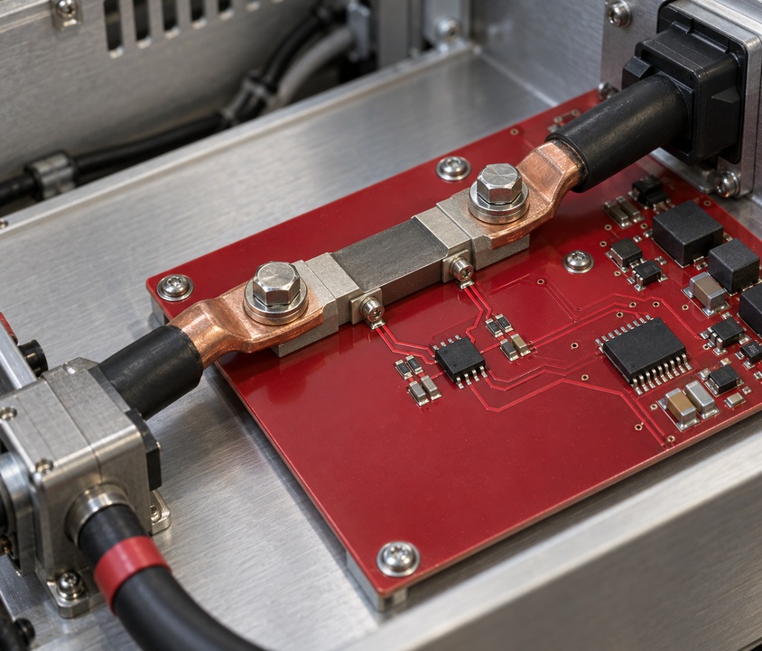
A practical guide to shunt resistor current measurement, covering resistance and power calculations, high-side and low-side sensing, two-terminal and four-terminal parts, Kelvin PCB layout, TCR, pulse …
An engineering guide to open-collector, open-drain and push-pull outputs, including pull-up resistor limits, rise-time calculations, wired logic, voltage translation and power-off checks.

Comparator circuit design covering voltage thresholds, input limits, open-collector outputs, LM393 wiring, op-amp differences, hysteresis, timing, window detection and practical fault diagnosis.

Schmitt triggers use separate rising and falling thresholds to stabilize slow or noisy signals. This guide covers hysteresis, 74HC14 and 74HCT14 selection, comparator calculations, RC oscillators and p…

Counterfeit components can hide behind convincing markings and passing basic function tests. This engineering reference covers source traceability, external inspection, X-ray, XRF, electrical testing, …

A practical engineering and sourcing framework covering lifecycle verification, lifetime-buy calculations, replacement qualification, supplier checks and counterfeit-risk controls.

TTL and CMOS logic families differ in thresholds, loading, output drive, power and timing. This engineering guide compares 74HC and 74HCT, calculates noise margins and checks 3.3 V/5 V compatibility.

A practical engineering guide to 3.3V and 5V logic compatibility, input thresholds, resistor dividers, translator ICs, MOSFET level shifting, I2C pull-ups, timing limits and power-sequencing risks.

The 74HC595 uses push-pull logic outputs, while the TPIC6B595 uses 50 V open-drain DMOS sinks for higher-power loads. This guide compares timing, current limits, 3.3 V interfacing, load wiring, thermal…

The 74HC595 converts serial data into eight stable parallel outputs. This guide covers pin functions, shift and storage timing, OE and MR behavior, drive-current limits, cascading, voltage compatibilit…


