
 My Inquiry
 My Account


Infineon Technologies ICE2QS03XKLA1
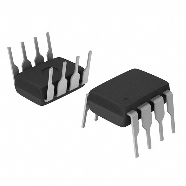
- Part No.:
- ICE2QS03XKLA1
- Manufacturer:
- Infineon Technologies
- Category:
- AC DC Converters, Offline Switches
- Package:
- 8-DIP (0.300", 7.62mm)
- Datasheet:
-
 ICE2QS03XKLA1.pdf
- Description:
- IC OFFLINE SWITCH FLYBACK 8DIP
- Quantity:
- Payment:

- Shipping:

Inventory:3,458
Please send an inquiry. Send us your inquiry, and we will respond immediately.
Product details
Overview
ICE2QS03XKLA1 from Infineon Technologies is a quasi-resonant (QR) AC-DC PWM controller IC designed for offline flyback converters in low-to-mid power SMPS applications. It integrates a 650 V avalanche-rated start-up cell, current-mode control, zero-current detection (ZCD), and built-in soft-start. Key specs include 65 kHz max switching frequency, <100 mW no-load power consumption, and operation up to 105 °C ambient temperature - enabling energy-efficient adapters and auxiliary supplies.
For engineers reviewing the ICE2QS03XKLA1 datasheet, ICE2QS03XKLA1 pinout, ICE2QS03XKLA1 application, or ICE2QS03XKLA1 equivalent, this controller supports design of compact, high-efficiency QR flyback converters with adaptive frequency foldback, precise overvoltage protection (OVP), and integrated brown-in/out hysteresis - critical for universal-input consumer and industrial power supplies.
Technical Context
The ICE2QS03XKLA1 implements quasi-resonant valley-switching control using ZCD to trigger MOSFET turn-on at the first drain voltage minimum after demagnetization, minimizing switching losses and EMI. Its current-mode architecture enables cycle-by-cycle peak current limiting and inherent slope compensation.
It features an integrated 650 V start-up circuit that eliminates external high-voltage resistors, and includes programmable OVP via external resistor divider, adjustable soft-start time, and thermal shutdown with hysteresis. The controller operates from 8.5–25 V VCC and supports both DCM and CCM flyback operation.
Key Specifications
| Parameter | Value and Actual Design Meaning |
|---|---|
| Topology Support | Quasi-resonant flyback - enables zero-voltage switching at light loads and reduced EMI. |
| Max Switching Frequency | 65 kHz - balances efficiency and transformer size for ≤30 W designs. |
| VCC Operating Range | 8.5–25 V - supports wide-range auxiliary winding regulation without external LDO. |
| No-Load Power Consumption | <100 mW at 230 VAC - meets EU CoC Tier 2 and DOE Level VI standby requirements. |
| Start-up Voltage | Integrated 650 V start-up cell - removes need for high-voltage start-up resistor network. |
| OVP Threshold Accuracy | ±3% - ensures reliable overvoltage protection with external resistor divider scaling. |
| Operating Ambient Temp | −40 to +105 °C - validated for enclosed industrial and automotive cabin-adjacent environments. |
Pinout & Package
ICE2QS03XKLA1 is housed in a compact 8-pin DSO-8 (3.9 mm × 4.9 mm) package with exposed thermal pad for enhanced thermal performance in high-density layouts.
| Pin/Terminal | Circuit Role | Design Meaning |
|---|---|---|
| VCC | Supply voltage input | Power rail for internal circuitry; clamped at 27.5 V; powers gate driver and control logic. |
| GND | Ground reference | Analog and power ground common point; requires low-inductance connection to PCB ground plane. |
| OUT | Gate drive output | Push-pull driver capable of sourcing/sinking 500 mA peak - directly drives CoolMOS™ or OptiMOS™ MOSFET gates. |
| ZCD | Zero-current detection input | Monitors auxiliary winding voltage to detect transformer demagnetization for valley switching timing. |
| CS | Current sense input | Receives signal from primary-side current-sense resistor; enables cycle-by-cycle overcurrent protection. |
| FB | Feedback input | Compares optocoupler-derived error signal to internal 2.5 V reference for closed-loop voltage regulation. |
| INV | Inverting input of error amplifier | Accepts feedback from secondary-side TL431 + optocoupler; sets regulation setpoint and loop gain. |
| NC | No connect | Internally unused pin; must be left floating or tied to GND per layout guidelines. |
Key Features
| Feature | Design Value |
|---|---|
| Integrated 650 V start-up cell | Eliminates external HV start-up resistor, reducing BOM count and board space by ~3 components. |
| Adaptive frequency foldback | Reduces switching frequency under light load to maintain >75% efficiency down to 10% load - critical for standby compliance. |
| Programmable overvoltage protection (OVP) | External resistor divider sets OVP threshold with ±3% accuracy - enables robust system-level safety without secondary sensing. |
| Brown-in/out hysteresis | Internal 0.5 V hysteresis on VCC monitors supply stability - prevents erratic restart during line dips or surges. |
| Thermal shutdown with hysteresis | Triggers at 150 °C junction temp with 20 °C hysteresis - protects MOSFET and transformer during overload or poor heatsinking. |
Applications
| USB-C Adapter | Smart Home Hub Power Supply |
|---|---|
|
Use Scenario: Compact 27 W USB-C PD adapter with universal AC input (90–264 VAC) and regulated 9 V/3 A output. IC Role / Device Role / Timing Role: Primary-side QR PWM controller managing flyback regulation, ZCD-based valley switching, and OVP/OTP protection. Use Value: Achieves <100 mW no-load consumption and <300 mW total standby loss - meeting strict global energy standards without auxiliary winding regulation IC. |
Use Scenario: Dual-output (5 V/12 V) auxiliary supply for Wi-Fi 6 gateway with isolated Ethernet PHY and Zigbee radio. IC Role / Device Role / Timing Role: Main controller for primary flyback stage delivering stable, low-noise 5 V rail; enables tight cross-regulation via coupled inductor design. Use Value: Integrated ZCD and current-mode control ensure stable operation across wide load transients (0–100% step) and variable line conditions typical in residential deployments. |
| Industrial Sensor Transmitter | LED Driver Auxiliary Supply |
|
Use Scenario: Loop-powered 4–20 mA sensor transmitter requiring isolated 3.3 V microcontroller supply from 24 VDC input. IC Role / Device Role / Timing Role: Flyback controller operating in DCM mode with fixed 65 kHz frequency and precise current limit for consistent startup under varying loop impedance. Use Value: Built-in thermal shutdown and brown-out hysteresis prevent malfunction during field-induced voltage sags or ambient temperature excursions up to 70 °C. |
Use Scenario: Constant-current LED driver with integrated MCU and isolated communication interface requiring clean 5 V auxiliary rail. IC Role / Device Role / Timing Role: Primary-side controller for flyback converter powering LED driver IC and UART isolation barrier. Use Value: <100 mW no-load power enables full-system compliance with IEC 62368-1 energy limits while maintaining fast transient response for digital dimming commands. |
Equivalent & Alternatives
The following parts are listed as comparable options for similar quasi-resonant flyback controller applications.
| Alternative Part | Technical Difference | Application Difference | Selection Advice |
|---|---|---|---|
| ICE2QS01G | Fixed 65 kHz frequency only; no adaptive foldback; no integrated start-up cell - requires external HV resistor. | Limited to fixed-frequency designs where light-load efficiency is less critical; higher BOM cost due to added start-up components. | Select when cost sensitivity outweighs no-load power targets and thermal derating is not required. |
| ICE5QSBG | Includes digital core, configurable via EEPROM; supports multiple protection modes and programmable soft-start; higher integration but larger footprint. | Suitable for platforms requiring field-programmable parameters or multi-rail sequencing; adds firmware overhead and programming infrastructure. | Choose for scalable platforms needing reconfigurable protection thresholds or future-proofing via firmware updates. |
Compared with ICE2QS03XKLA1, ICE2QS01G sacrifices efficiency and integration for lower unit cost, while ICE5QSBG trades simplicity and footprint for configurability and advanced diagnostics - making ICE2QS03XKLA1 optimal for cost-constrained, high-volume, energy-compliant flyback designs.
Availability
ICE2QS03XKLA1 is available at Aetrix Electronics and suitable for USB-C adapters, smart home hub power supplies, industrial sensor transmitters, and LED driver auxiliary supplies requiring stable component supply, long-term lifecycle support, and compliance with international energy regulations.
Supply support for ICE2QS03XKLA1 includes scheduled delivery planning, volume procurement assistance, BOM continuity management, traceable sourcing, and lifecycle availability coordination for OEM customers, industrial embedded developers, connected-device designers, and electronics production programs.
Manufacturer
Infineon Technologies is a German semiconductor manufacturer specializing in power management, automotive, and industrial control ICs, with leadership in CoolMOS™, OptiMOS™, and EiceDRIVER™ product families.
ICE2QS03XKLA1 belongs to Infineon's ICE2Q family of quasi-resonant flyback controllers, engineered specifically for high-efficiency, low-standby-power AC-DC conversion in consumer and industrial power supplies.
FAQ
What is the recommended minimum ZCD resistor value for reliable valley detection?
The ZCD pin requires a resistor divider from the auxiliary winding to limit input current to ≤10 µA. For a typical 12 V auxiliary winding, a 1 MΩ top resistor with 100 kΩ bottom resistor provides sufficient signal amplitude and noise immunity while staying within the 10 µA absolute maximum rating - verified in Infineon's AN2018-09 application note.
Does ICE2QS03XKLA1 support synchronous rectification?
No, ICE2QS03XKLA1 does not include SR control outputs or timing signals for external synchronous rectifier drivers. It is designed for diode-rectified flyback topologies. For SR-enabled designs, Infineon recommends pairing it with dedicated SR controllers like IRS21850 or using the ICE5QSBG family with integrated SR gate drive.
Can the FB pin be used for primary-side regulation without an optocoupler?
No - the FB pin is designed exclusively for optocoupler-coupled secondary-side feedback. It compares the incoming signal against an internal 2.5 V reference and lacks primary-side compensation circuitry or auxiliary winding compensation capability. Primary-side regulation requires dedicated PSR controllers such as ICE3Bxx series.
What is the maximum allowable VCC ripple before instability occurs?
VCC ripple must remain below 1.5 Vpp to avoid false triggering of the brown-out comparator. Layout best practices include placing a 10 µF low-ESR electrolytic capacitor plus a 100 nF ceramic capacitor directly at the VCC pin, with short traces to minimize inductance - confirmed in Infineon's ICE2QS03XKLA1 evaluation board layout guidelines.
ICE2QS03XKLA1 Specifications
- Product attributes
- Attribute value
- Manufacturer:
- Infineon Technologies
- Series:
- -
- Package/Case:
- 8-DIP (0.300", 7.62mm)
- Packaging:
- Tube
- Product Status:
- Obsolete
- Output Isolation:
- Isolated
- Internal Switch(s):
- No
- Voltage - Breakdown:
- -
- Topology:
- Flyback
- Voltage - Start Up:
- 18 V
- Voltage - Supply (Vcc/Vdd):
- 10.5V ~ 27V
- Duty Cycle:
- 50%
- Frequency - Switching:
- 52kHz
- Power (Watts):
- -
- Fault Protection:
- Current Limiting, Open Loop, Over Load, Over Voltage
- Control Features:
- -
- Operating Temperature:
- -40°C ~ 125°C (TJ)
- Grade:
- -
- Qualification:
- -
- Supplier Device Package:
- PG-DIP-8
- Mounting Type:
- Through Hole
ICE2QS03XKLA1 FAQ
1.How can I place an order for ICE2QS03XKLA1 through Aetrix?
Please submit a Request for Quotation (RFQ) for ICE2QS03XKLA1 on Aetrix. Our sales agent will provide a competitive quotation and guide you through the order confirmation once you accept the terms.
2.Are the price and stock information for ICE2QS03XKLA1 reliable?
The price and inventory of ICE2QS03XKLA1 are updated periodically and may fluctuate due to market conditions. Stock and pricing data are typically refreshed every 24 hours. Quotation validity for ICE2QS03XKLA1 is usually 5 days.
3.What payment methods are accepted for ICE2QS03XKLA1?
We accept Wire Transfer, PayPal, Credit Card, Western Union, MoneyGram, and Escrow for ICE2QS03XKLA1 transactions.
Note: Certain payment methods may incur a processing fee.
4.How is shipping managed for ICE2QS03XKLA1?
ICE2QS03XKLA1 orders can be shipped via leading logistics carriers, including DHL, UPS, FedEx, TNT, or Registered Mail.
Once your ICE2QS03XKLA1 order is processed, you will receive an email with the shipment details and tracking number.
Note: Tracking information may take up to 24 hours to appear. Express delivery typically takes 3–5 business days.
5.How can I obtain technical support or documentation for ICE2QS03XKLA1?
For technical support, including ICE2QS03XKLA1 datasheets, pinout diagrams, or application guidance, please contact our engineering support team. They can provide detailed documentation and assistance for your ICE2QS03XKLA1 requirements.
6.How does Aetrix verify that ICE2QS03XKLA1 is sourced from the original manufacturer or authorized distributors?
All ICE2QS03XKLA1 products on Aetrix are procured from qualified distributors and authorized channels. Our dedicated quality assurance team conducts strict verification, including traceability checks and, if necessary, third-party testing. This ensures that ICE2QS03XKLA1 meets industry standards.
7.What is the process for return or replacement of ICE2QS03XKLA1?
All ICE2QS03XKLA1 units undergo pre-shipment inspection (PSI). If there is an issue with ICE2QS03XKLA1, returns or replacements are accepted under the following conditions:
1.Quantity discrepancies, incorrect items, or visible external defects (such as breakage or corrosion), acknowledged by Aetrix.
2.The issue is reported within 90 days of delivery.
3.The ICE2QS03XKLA1 part is unused and in its original packaging.
Return procedure for ICE2QS03XKLA1:
1.Submit a request within 90 days.
2.Obtain a Return Material Authorization (RMA) from Aetrix.
ICE2QS03XKLA1 Tags
-
LNK6407D-TL
Power Integrations
-
LNK3204D-TL
Power Integrations

-
SR10LG-G
Microchip Technology
-
TNY285DG-TL
Power Integrations
-
LNK304DN-TL
Power Integrations
-
TNY285KG-TL
Power Integrations
-
LNK3206D-TL
Power Integrations
-
LNK623DG-TL
Power Integrations
-
TNY286PG
Power Integrations
-
LNK624DG-TL
Power Integrations
-
LNK604DG-TL
Power Integrations

-
UCC28704DBVR-1
Texas Instruments
Tech Hub

18650 battery guide covering lithium-ion cell basics, 3.6V/3.7V voltage, 4.2V charging, mAh and Wh capacity, protected cells, chargers, BMS, series-parallel packs, holders, welding and sourcing checks.…

Hall effect sensor guide covering working principle, linear and digital sensors, Arduino circuits, current sensing, speed detection, automotive applications, A3144 examples, signal filtering and datash…

Product Change Notification guide for electronic components, covering PCN meaning, PCN vs PDN/EOL, common change types, risk levels, form-fit-function review, engineering validation, BOM control, LTB/L…

A practical guide to blend door actuators, covering HVAC function, symptoms, location, AC and heater issues, reset and calibration, replacement cost, electrical diagnosis, compatibility checks, and rep…

Engineering guide to Raspberry Pi alternatives, covering chip-level differences, Orange Pi, ROCK, Jetson, Banana Pi, NanoPi, Compute Module, Pico, GPIO, camera, HAT compatibility, and replacement risks…

Engineering guide to dynamic load response testing for high-current buck converters, covering load step setup, slew rate, Vcore undershoot, overshoot, recovery time, probe location, output capacitors a…

Engineering guide to output capacitor selection for ASIC Vcore rails, covering bulk capacitors, polymer capacitors, MLCC decoupling, DC bias, ESR, ESL, placement, transient response and substitution ri…

Engineering guide to high-current ASIC Vcore rails, covering 12-phase buck architecture, PMBus control, dynamic load testing, output capacitor networks, smart power stage selection, thermal design and …

Voltage regulator guide covering linear, LDO, 7805, Zener, adjustable, buck, VRM and alternator regulators, with design checks, testing methods, troubleshooting and datasheet-based selection.

Amplifier guide covering voltage, current and power amplification, gain, feedback, amplifier classes, audio and RF applications, op-amp circuits, transimpedance amplifiers, datasheet selection and trou…


