
 My Inquiry
 My Account


Cypress Semiconductor Corp S29PL127J80BFI010
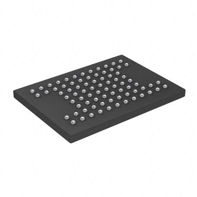
- Part No.:
- S29PL127J80BFI010
- Manufacturer:
- Cypress Semiconductor Corp
- Category:
- Memory
- Package:
- 80-VFBGA
- Datasheet:
-
 S29PL127J80BFI010.pdf
- Description:
- IC FLASH 128MBIT PARALLEL 80FBGA
- Quantity:
- Payment:

- Shipping:

Inventory:2,189
Please send an inquiry. Send us your inquiry, and we will respond immediately.
Product details
Overview
S29PL127J80BFI010 from Infineon Technologies (formerly Cypress) is a 128-Mbit (8 Mword × 16-bit), 3.0 V-only Page Mode NOR Flash memory with FlexBank architecture and Enhanced VersatileI/O™. It supports simultaneous read/write across four independent banks, features 20 ns page access, 55 ns random access, and operates across 2.7–3.6 V for battery-powered embedded systems requiring nonvolatile code storage and in-system reprogramming.
For engineers reviewing the S29PL127J80BFI010 datasheet, S29PL127J80BFI010 pinout, S29PL127J80BFI010 application, or S29PL127J80BFI010 equivalent, key selection criteria include bank-level concurrency, 1.8 V/3.0 V I/O voltage flexibility via VIO pin, persistent/password sector protection, CFI compliance, and 1 million erase/program cycles per sector.
Technical Context
This device implements a 4-bank FlexBank architecture enabling true zero-latency concurrent read and program/erase operations - e.g., reading from Bank A while erasing Bank C. Each bank supports independent command execution, with Bank A and D sized at 16 Mbit (4 Kw × 8 + 32 Kw × 31) and Banks B/C at 48 Mbit (32 Kw × 96) each.
Enhanced VersatileI/O™ decouples I/O voltage from core VCC: VIO pin sets output drive level and input tolerance to either 1.8 V or 3.0 V, allowing seamless interfacing with mixed-voltage SoCs. Sector protection includes both persistent (PPB-based) and password-locked modes, with up to 128-word Secured Silicon Sector accessible via command sequence.
Key Specifications
| Parameter | Value and Actual Design Meaning |
|---|---|
| Memory Density | 128 Mbit (8 Mwords × 16-bit data bus) |
| Supply Voltage Range | 2.7–3.6 V - enables direct integration into 3.3 V and Li-ion battery-powered systems without level-shifting |
| Page Access Time | 20 ns - enables high-speed instruction fetch from cached pages within same 8-word boundary |
| Random Access Time | 55 ns - determines worst-case latency for non-sequential address jumps |
| Erase/Program Endurance | 1 million cycles per sector - supports field firmware updates over product lifetime |
| Data Retention | 20 years typical - ensures long-term reliability in industrial and automotive environments |
| VIO Options | 1.8 V or 3.0 V - allows dynamic I/O voltage selection to match host processor interface requirements |
Pinout & Package
Package: 80-ball Fine-pitch BGA (VBG080), 11 mm × 8 mm footprint, 0.5 mm pitch, RoHS-compliant.
| Pin/Terminal | Circuit Role | Design Meaning |
|---|---|---|
| A0–A21 | Address Inputs | 22-bit address bus supporting full 8 Mword addressing; A0–A1 select byte within 16-bit word |
| DQ0–DQ15 | Data I/O | 16-bit bidirectional data bus; direction controlled by CE#, OE#, and WE# timing |
| CE# | Chip Enable | Active-low chip select; device enters standby when deasserted during read/write |
| OE# | Output Enable | Active-low control for data bus drivers; enables read data output without affecting internal state |
| WE# | Write Enable | Active-low strobe for latching addresses/data during command sequences and programming |
| RY/BY# | Ready/Busy Output | Open-drain status indicator - low during active program/erase, high when ready for next command |
| RESET# | Hardware Reset | Active-low asynchronous reset that forces device into reading array mode, clearing pending commands |
| WP#/ACC | Write Protect/Acceleration | VIL = hardware lock on top/bottom 4K-word sectors; VIH = unlock; VHH = factory accelerated programming mode |
| VIO | I/O Voltage Reference | Defines output drive strength and input threshold - set to 1.8 V or 3.0 V to match host interface voltage |
Key Features
| Feature | Design Value |
|---|---|
| FlexBank Architecture | Four independent banks enable concurrent read from one bank while erasing/programming another - eliminates CPU wait states in real-time firmware update scenarios |
| Enhanced VersatileI/O™ | VIO pin configures all I/Os (DQ0–DQ15, control pins) to operate at either 1.8 V or 3.0 V - eliminates external level shifters in mixed-voltage designs |
| Secured Silicon Sector | 128-word factory-accessible region with 64-word customer-lockable space - supports secure boot key storage and cryptographic parameter retention |
| CFI Compliance | JEDEC JESD68-compliant interface provides standardized register map for automatic flash detection and configuration in bootloader software |
| Erase/Program Suspend | Pause ongoing erase or program operation to service urgent read requests - maintains system responsiveness during background flash maintenance |
Applications
| Industrial HMI Firmware Storage | Automotive ADAS Boot Memory |
|---|---|
Use Scenario: Storing GUI assets, configuration tables, and application firmware in programmable HMIs with periodic field updates. IC Role / Device Role / Timing Role: Nonvolatile code/data storage with in-system reprogrammability and hardware write protection against accidental corruption. Use Value: Persistent Sector Protection locks critical boot sectors while allowing user-defined update partitions - ensuring UI stability across 10+ years of operation. | Use Scenario: Holding boot code and safety-critical calibration data for radar/EPS ECUs requiring AEC-Q100 compliance. IC Role / Device Role / Timing Role: Primary boot memory with deterministic 55 ns random access and 20-year data retention under thermal stress. Use Value: Password Sector Protection prevents unauthorized firmware modification - meeting ISO 26262 ASIL-B integrity requirements for secure boot verification. |
| Medical Imaging System BIOS | Telecom Base Station Configuration |
Use Scenario: Storing FPGA configuration bitstreams and diagnostic firmware in portable ultrasound devices with battery backup. IC Role / Device Role / Timing Role: Low-power (0.2 µA standby) NOR Flash supporting fast wake-from-sleep code execution via page-mode reads. Use Value: 2.7–3.6 V operation matches Li-ion battery discharge curve - eliminating need for auxiliary LDO regulation during brownout conditions. | Use Scenario: Hosting FPGA configuration, DSP firmware, and network protocol stacks in carrier-grade baseband units. IC Role / Device Role / Timing Role: High-reliability code storage with simultaneous read/write enabling hot firmware patching without service interruption. Use Value: Four-bank FlexBank allows background sector erase while serving live traffic data - achieving >99.999% uptime during field upgrades. |
Equivalent & Alternatives
The following parts are listed as comparable options for similar NOR Flash memory applications.
| Alternative Part | Technical Difference | Application Difference | Selection Advice |
|---|---|---|---|
| S29GL128S90TFI010 | 128 Mbit, 3.0 V, 90 nm process; lacks VersatileI/O™ and FlexBank concurrency - single-bank architecture only | No simultaneous read/write; slower effective throughput in firmware update scenarios | Select when cost sensitivity outweighs concurrency needs and 1.8 V I/O is not required |
| MX29GL128FHT2I-90G | 128 Mbit, 3.0 V, 65 nm process; supports CFI and sector protection but no password-secured silicon region | Lacks 128-word secured sector for cryptographic keys - requires external secure element for boot authentication | Select when external security IC is already deployed and higher endurance (3M cycles) is prioritized |
Compared with S29GL128S90TFI010 and MX29GL128FHT2I-90G, the S29PL127J80BFI010 uniquely delivers concurrent bank operation, VIO-configurable I/O, and integrated secured silicon - making it optimal for systems requiring real-time firmware agility, mixed-voltage compatibility, and on-die security primitives.
Availability
S29PL127J80BFI010 is available at Aetrix Electronics and suitable for industrial HMI firmware storage, automotive ADAS boot memory, and medical imaging system BIOS requiring stable component supply and long-term lifecycle support.
Supply support for S29PL127J80BFI010 includes scheduled delivery planning, volume procurement assistance, BOM continuity management, traceable sourcing, and lifecycle availability coordination for OEM customers, industrial embedded developers, connected-device designers, and electronics production programs.
Manufacturer
Infineon Technologies is a global semiconductor leader headquartered in Munich, Germany, specializing in power management, sensor, and memory solutions for industrial, automotive, and IoT applications.
The S29PL-J series was originally developed by Cypress and continues under Infineon's NOR Flash portfolio, targeting high-reliability embedded systems needing concurrent execution, flexible I/O voltage, and robust security features for code storage and firmware updates.
FAQ
What is the function of the VIO pin on S29PL127J80BFI010?
The VIO pin sets the I/O voltage reference for all data and control pins (DQ0–DQ15, CE#, OE#, WE#, RY/BY#, RESET#, WP#/ACC). When tied to 1.8 V, outputs drive to 1.8 V levels and inputs tolerate 1.8 V logic thresholds; when tied to 3.0 V, they operate at 3.0 V levels. This eliminates external level shifters in mixed-voltage SoC interfaces.
Does S29PL127J80BFI010 support true simultaneous read and write across different banks?
Yes. Its FlexBank architecture divides memory into four physically independent banks (A–D). The device can execute an erase or program operation in one bank while simultaneously performing read operations in another bank - with zero latency switching and no performance penalty, verified in the datasheet's Simultaneous Read/Write Block Diagram (page 10).
How does Password Sector Protection differ from Persistent Sector Protection?
Password Sector Protection uses a user-defined 64-bit password to lock/unlock sector groups, requiring password entry before modification - ideal for secure boot partitioning. Persistent Sector Protection uses hardware-latched PPB bits that remain locked after power cycle unless explicitly cleared via unlock command - suited for permanent factory-set protection of critical firmware regions.
What package variants are available for the S29PL127J family?
The S29PL127J80BFI010 is exclusively offered in the 80-ball Fine-pitch BGA (VBG080, 11 mm × 8 mm). Other members include PL064J/PL032J in 48-ball BGA (VBK048, 8.15 mm × 6.15 mm) and PL127J in 56-pin TSOP (TS056, 20 mm × 14 mm), but S29PL127J80BFI010 is BGA-only per ordering information (page 6 of datasheet 002-00615 Rev. *F).
S29PL127J80BFI010 Specifications
- Product attributes
- Attribute value
- Manufacturer:
- Cypress Semiconductor Corp
- Series:
- PL-J
- Package/Case:
- 80-VFBGA
- Packaging:
- Bulk
- Product Status:
- Obsolete
- Programmable:
- Not Verified
- Memory Type:
- Non-Volatile
- Memory Format:
- FLASH
- Technology:
- FLASH - NOR
- Memory Size:
- 128Mbit
- Memory Organization:
- 8M x 16
- Memory Interface:
- Parallel
- Clock Frequency:
- -
- Write Cycle Time - Word, Page:
- 80ns
- Access Time:
- 80 ns
- Voltage - Supply:
- 1.65V ~ 1.95V
- Operating Temperature:
- -40°C ~ 85°C (TA)
- Grade:
- -
- Qualification:
- -
- Mounting Type:
- Surface Mount
- Supplier Device Package:
- 80-FBGA (8x11)
S29PL127J80BFI010 FAQ
1.How can I place an order for S29PL127J80BFI010 through Aetrix?
Please submit a Request for Quotation (RFQ) for S29PL127J80BFI010 on Aetrix. Our sales agent will provide a competitive quotation and guide you through the order confirmation once you accept the terms.
2.Are the price and stock information for S29PL127J80BFI010 reliable?
The price and inventory of S29PL127J80BFI010 are updated periodically and may fluctuate due to market conditions. Stock and pricing data are typically refreshed every 24 hours. Quotation validity for S29PL127J80BFI010 is usually 5 days.
3.What payment methods are accepted for S29PL127J80BFI010?
We accept Wire Transfer, PayPal, Credit Card, Western Union, MoneyGram, and Escrow for S29PL127J80BFI010 transactions.
Note: Certain payment methods may incur a processing fee.
4.How is shipping managed for S29PL127J80BFI010?
S29PL127J80BFI010 orders can be shipped via leading logistics carriers, including DHL, UPS, FedEx, TNT, or Registered Mail.
Once your S29PL127J80BFI010 order is processed, you will receive an email with the shipment details and tracking number.
Note: Tracking information may take up to 24 hours to appear. Express delivery typically takes 3–5 business days.
5.How can I obtain technical support or documentation for S29PL127J80BFI010?
For technical support, including S29PL127J80BFI010 datasheets, pinout diagrams, or application guidance, please contact our engineering support team. They can provide detailed documentation and assistance for your S29PL127J80BFI010 requirements.
6.How does Aetrix verify that S29PL127J80BFI010 is sourced from the original manufacturer or authorized distributors?
All S29PL127J80BFI010 products on Aetrix are procured from qualified distributors and authorized channels. Our dedicated quality assurance team conducts strict verification, including traceability checks and, if necessary, third-party testing. This ensures that S29PL127J80BFI010 meets industry standards.
7.What is the process for return or replacement of S29PL127J80BFI010?
All S29PL127J80BFI010 units undergo pre-shipment inspection (PSI). If there is an issue with S29PL127J80BFI010, returns or replacements are accepted under the following conditions:
1.Quantity discrepancies, incorrect items, or visible external defects (such as breakage or corrosion), acknowledged by Aetrix.
2.The issue is reported within 90 days of delivery.
3.The S29PL127J80BFI010 part is unused and in its original packaging.
Return procedure for S29PL127J80BFI010:
1.Submit a request within 90 days.
2.Obtain a Return Material Authorization (RMA) from Aetrix.
S29PL127J80BFI010 Tags

-
M24C02-WMN6TP
STMicroelectronics

-
AT24C02C-XHM-T
Microchip Technology

-
AT21CS01-STUM10-T
Microchip Technology

-
AT24C02C-SSHM-T
Microchip Technology

-
24LC01BT-I/OT
Microchip Technology

-
M24C02-FMC6TG
STMicroelectronics
-
AT24CS02-SSHM-T
Microchip Technology

-
93LC46BT-I/OT
Microchip Technology
-
AT24C04C-SSHM-T
Microchip Technology

-
24LC01BT-I/SN
Microchip Technology
-
24AA02UIDT-I/OT
Microchip Technology

-
AT24C08C-STUM-T
Microchip Technology
Tech Hub

Hall effect sensor guide covering working principle, linear and digital sensors, Arduino circuits, current sensing, speed detection, automotive applications, A3144 examples, signal filtering and datash…

Product Change Notification guide for electronic components, covering PCN meaning, PCN vs PDN/EOL, common change types, risk levels, form-fit-function review, engineering validation, BOM control, LTB/L…

A practical guide to blend door actuators, covering HVAC function, symptoms, location, AC and heater issues, reset and calibration, replacement cost, electrical diagnosis, compatibility checks, and rep…

Engineering guide to Raspberry Pi alternatives, covering chip-level differences, Orange Pi, ROCK, Jetson, Banana Pi, NanoPi, Compute Module, Pico, GPIO, camera, HAT compatibility, and replacement risks…

Engineering guide to dynamic load response testing for high-current buck converters, covering load step setup, slew rate, Vcore undershoot, overshoot, recovery time, probe location, output capacitors a…

Engineering guide to output capacitor selection for ASIC Vcore rails, covering bulk capacitors, polymer capacitors, MLCC decoupling, DC bias, ESR, ESL, placement, transient response and substitution ri…

Engineering guide to high-current ASIC Vcore rails, covering 12-phase buck architecture, PMBus control, dynamic load testing, output capacitor networks, smart power stage selection, thermal design and …

Voltage regulator guide covering linear, LDO, 7805, Zener, adjustable, buck, VRM and alternator regulators, with design checks, testing methods, troubleshooting and datasheet-based selection.

Amplifier guide covering voltage, current and power amplification, gain, feedback, amplifier classes, audio and RF applications, op-amp circuits, transimpedance amplifiers, datasheet selection and trou…

Machine vision system guide covering components, inspection workflow, camera and lens selection, FOV, pixel resolution, motion blur, strobe lighting, bandwidth, 2D/3D vision, integration, troubleshooti…


