
 My Inquiry
 My Account


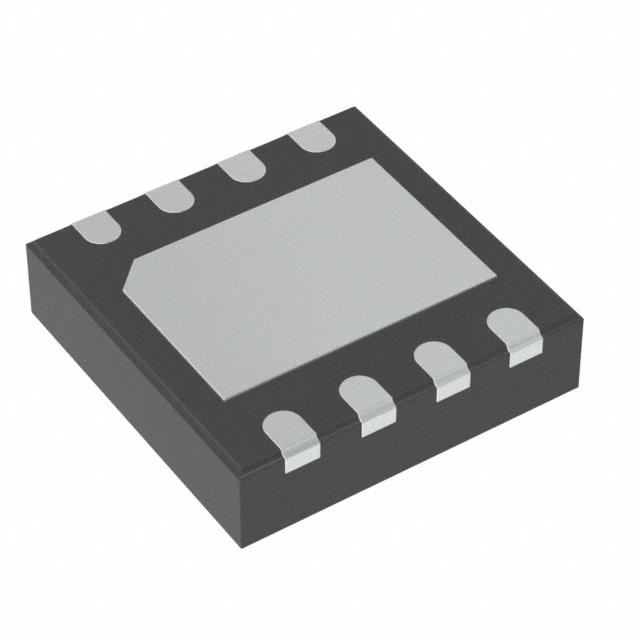
Infineon Technologies TLE6251DSXUMA2
- Part No.:
- TLE6251DSXUMA2
- Manufacturer:
- Infineon Technologies
- Category:
- Drivers, Receivers, Transceivers
- Package:
- 8-SOIC (0.154", 3.90mm Width)
- Datasheet:
-
 TLE6251DSXUMA2.pdf
- Description:
- IC TRANSCEIVER FULL 1/1 PGDSO8
- Quantity:
- Payment:

- Shipping:

Inventory:5,642
Please send an inquiry. Send us your inquiry, and we will respond immediately.
Product details
Overview
TLE6251DSXUMA2 from Infineon Technologies is a high-speed CAN transceiver in PG-DSO-8 package, serving as the physical layer interface between CAN protocol controllers and differential bus lines per ISO/DIS 11898. It supports up to 1 Mbaud data rate, operates across 12 V and 24 V automotive systems, features bus wake-up capability via RxD level change in standby mode, and includes TxD time-out, overtemperature protection, and split termination for recessive-level stabilization - deployed in body control modules and powertrain gateways.
For engineers reviewing the TLE6251DSXUMA2 datasheet, TLE6251DSXUMA2 pinout, TLE6251DSXUMA2 application, or TLE6251DSXUMA2 equivalent, key selection considerations include wake-up sensitivity in mixed-power networks, passive bus behavior during STB-controlled standby, CANH/CANL short-circuit robustness to battery/ground/VCC, and compatibility with 3.3 V/5 V logic controllers in harsh automotive environments.
Technical Context
The TLE6251DSXUMA2 implements a dual-mode architecture (normal/standby) controlled by the STB pin, where standby mode disables driver/receiver stages while retaining wake-up detection via differential bus activity. Its Smart Power Technology SPT® integrates bipolar/CMOS control with DMOS power devices on a single die.
Wake-up signaling occurs through RxD level transitions synchronized to bus state changes, not edge-triggered interrupts; the split termination output stabilizes recessive common-mode voltage without external resistors, and the TxD time-out function disables transmission after >120 µs dominant state to prevent bus lockup.
Key Specifications
| Parameter | Value and Actual Design Meaning |
|---|---|
| Data Rate | Up to 1 Mbaud - enables real-time communication in powertrain and chassis control networks. |
| Bus Voltage Range | 12 V and 24 V automotive systems - supports both passenger car and commercial vehicle electrical architectures. |
| Standby Current | < 30 µA - minimizes quiescent load in always-on ECU nodes with partial network wake-up. |
| Common Mode Range | −2 V to +14 V - ensures immunity against electromagnetic interference in noisy engine compartments. |
| Short-Circuit Protection | CANH/CANL protected to ground, battery, and VCC - prevents latch-up or destruction during wiring faults. |
| Logic Compatibility | 3.3 V and 5 V digital inputs - interoperable with legacy and modern microcontrollers without level-shifting. |
| Thermal Shutdown | Activates above 175 °C - disables driver stages until TxD sees dominant-to-recessive transition, preventing bit errors on recovery. |
Pinout & Package
Package: PG-DSO-8 (plastic dual small outline, 8-pin, exposed pad, RoHS-compliant).
| Pin/Terminal | Circuit Role | Design Meaning |
|---|---|---|
| 1 TxD | Transmit data input | 20 kΩ internal pull-up; dominant state = LOW - interfaces directly with MCU TX pin without external biasing. |
| 2 GND | Ground reference | Primary return path for VCC, CANH, CANL, and RxD - requires low-inductance connection to minimize EMI. |
| 3 VCC | 5 V supply input | Must be decoupled with 100 nF ceramic capacitor to GND - powers internal logic and driver stages. |
| 4 RxD | Receive data output | LOW in dominant state; signals wake-up via level change during standby - connects to MCU RX pin. |
| 5 SPLIT | Split termination output | Drives external 60 Ω resistor midpoint to stabilize recessive common-mode voltage - eliminates need for two 120 Ω terminations. |
| 6 CANL | Low-side bus line | Differential input/output; LOW in dominant state - connects to CAN bus low wire with ESD protection. |
| 7 CANH | High-side bus line | Differential input/output; HIGH in dominant state - connects to CAN bus high wire with fault tolerance to ±40 V transients. |
| 8 STB | Standby mode control | Internal pull-up; LOW = normal mode, HIGH = standby - enables selective node sleep/wake in multi-ECU networks. |
Key Features
| Feature | Design Value |
|---|---|
| Remote wake-up via CAN bus | RxD level toggles synchronously with bus state during standby - allows full-network wake without dedicated wake-line wiring. |
| No bus load in standby | Driver and receiver fully disabled; only wake-detection circuit active - preserves bus integrity in mixed-power networks. |
| Split termination support | SPLIT pin drives center-tap of 60 Ω termination - reduces component count and improves recessive-level stability vs. discrete 120 Ω terminators. |
| TxD time-out protection | Auto-disable after >120 µs dominant TxD - prevents permanent bus dominance due to MCU lockup or firmware error. |
| AEC-Q100 qualified | Qualified per Grade 1 (−40 °C to +125 °C ambient) - validated for under-hood and cabin-mounted automotive ECUs. |
Applications
| Body Control Module (BCM) | Powertrain Gateway |
|---|---|
Use Scenario: Centralized lighting, door lock, and window control in modern vehicles with distributed CAN nodes. IC Role / Device Role / Timing Role: Physical layer transceiver enabling bidirectional message exchange between BCM MCU and peripheral nodes at 500 kbaud. Use Value: Standby mode reduces system current by >99% during ignition-off, extending battery life without sacrificing remote wake-up responsiveness. | Use Scenario: Aggregating CAN messages between engine, transmission, and chassis domains in multi-bus architectures. IC Role / Device Role / Timing Role: High-speed interface bridging 1 Mbaud powertrain CAN FD subnets to lower-speed body networks. Use Value: Split termination maintains signal integrity across long harness runs, reducing bit error rate in high-noise drivetrain environments. |
| Advanced Driver Assistance System (ADAS) Sensor Hub | Electric Vehicle Battery Management System (BMS) |
Use Scenario: Consolidating radar, camera, and ultrasonic sensor data into a central ADAS domain controller. IC Role / Device Role / Timing Role: Robust CAN physical interface handling transient-rich sensor harnesses near motors and inverters. Use Value: Overtemperature shutdown and CANH/CANL short-circuit protection prevent failure during thermal stress events in front-end mounting locations. | Use Scenario: Interfacing cell monitoring ICs and pack controllers across high-voltage battery enclosures with isolation barriers. IC Role / Device Role / Timing Role: Isolated CAN node transceiver operating from local 5 V rail, communicating SOC/SOH status at 125 kbaud. Use Value: Wide common-mode range (−2 V to +14 V) rejects ground-loop noise between isolated battery modules and main controller. |
Equivalent & Alternatives
The following parts are listed as comparable options for similar high-speed CAN transceiver applications.
| Alternative Part | Technical Difference | Application Difference | Selection Advice |
|---|---|---|---|
| NXP TJA1042T/3 | Lower standby current (15 µA), integrated VIO supply for 3.3 V logic, no SPLIT pin | Requires external 120 Ω terminators; better suited for compact PCB layouts with space-constrained routing | Select when lowest quiescent power and 3.3 V MCU interface are prioritized over split-termination simplicity |
| ST TJA1055T | Extended common-mode range (−7 V to +18 V), no wake-up via RxD, higher ESD rating (±8 kV HBM) | Lacks bus wake-up; used in non-sleeping nodes like infotainment gateways requiring enhanced ESD robustness | Select when ESD immunity and extended voltage tolerance outweigh remote wake-up requirement |
Compared with TJA1042T/3 and TJA1055T, the TLE6251DSXUMA2 uniquely combines bus-initiated wake-up, split termination, and AEC-Q100 Grade 1 qualification - making it optimal for cost-sensitive, thermally demanding, and partially powered automotive nodes where bus-level coordination is critical.
Availability
TLE6251DSXUMA2 is available at Aetrix Electronics and suitable for body control modules, powertrain gateways, ADAS sensor hubs, and EV battery management systems requiring stable component supply across automotive production lifecycles.
Supply support for TLE6251DSXUMA2 includes scheduled delivery planning, volume procurement assistance, BOM continuity management, traceable sourcing, and lifecycle availability coordination for OEM customers, industrial embedded developers, connected-device designers, and electronics production programs.
Manufacturer
Infineon Technologies AG is a German semiconductor manufacturer specializing in power management, automotive electronics, and security solutions, with global R&D and manufacturing infrastructure.
The TLE6251DSXUMA2 belongs to Infineon's automotive CAN transceiver product line, designed specifically for robust, low-power, and wake-up-capable HS-CAN communication in safety-critical vehicle networks.
FAQ
What is the purpose of the SPLIT pin on the TLE6251DSXUMA2?
The SPLIT pin outputs a reference voltage to drive the center tap of an external 60 Ω termination resistor, stabilizing the recessive common-mode voltage on the CAN bus. This eliminates the need for two separate 120 Ω terminators and improves signal integrity in long or noisy harnesses, especially in automotive applications where EMI immunity is critical.
How does wake-up work in standby mode?
In standby mode, the TLE6251DSXUMA2 disables its driver and receiver but keeps the wake-up detection circuit active. When bus activity occurs, the RxD pin changes level synchronously with the bus dominant/recessive state - this level transition serves as the wake-up flag for the connected MCU, requiring no additional wake-line hardware.
Is the TLE6251DSXUMA2 compatible with 3.3 V microcontrollers?
Yes - the TLE6251DSXUMA2's TxD input and RxD output are compatible with both 3.3 V and 5 V logic levels. The TxD pin has a 20 kΩ internal pull-up, and RxD drives standard CMOS-compatible levels, allowing direct interfacing with modern low-voltage MCUs without level-shifting circuitry.
What happens during overtemperature shutdown?
When junction temperature exceeds ~175 °C, the driver stages deactivate to protect the device. Transmission resumes only after the TxD input transitions from dominant to recessive - this prevents bit errors that could occur if the driver re-enabled mid-bit. The receiver remains functional to detect wake-up signals during thermal recovery.
TLE6251DSXUMA2 Specifications
- Product attributes
- Attribute value
- Manufacturer:
- Infineon Technologies
- Series:
- -
- Package/Case:
- 8-SOIC (0.154", 3.90mm Width)
- Packaging:
- Tape & Reel (TR)
- Product Status:
- Not For New Designs
- Type:
- Transceiver
- Protocol:
- CANbus
- Number of Drivers/Receivers:
- 1/1
- Duplex:
- Full
- Receiver Hysteresis:
- 200 mV
- Data Rate:
- 1MBd
- Voltage - Supply:
- 4.75V ~ 5.25V
- Operating Temperature:
- -40°C ~ 150°C
- Grade:
- -
- Qualification:
- -
- Mounting Type:
- Surface Mount
- Supplier Device Package:
- PG-DSO-8
TLE6251DSXUMA2 FAQ
1.How can I place an order for TLE6251DSXUMA2 through Aetrix?
Please submit a Request for Quotation (RFQ) for TLE6251DSXUMA2 on Aetrix. Our sales agent will provide a competitive quotation and guide you through the order confirmation once you accept the terms.
2.Are the price and stock information for TLE6251DSXUMA2 reliable?
The price and inventory of TLE6251DSXUMA2 are updated periodically and may fluctuate due to market conditions. Stock and pricing data are typically refreshed every 24 hours. Quotation validity for TLE6251DSXUMA2 is usually 5 days.
3.What payment methods are accepted for TLE6251DSXUMA2?
We accept Wire Transfer, PayPal, Credit Card, Western Union, MoneyGram, and Escrow for TLE6251DSXUMA2 transactions.
Note: Certain payment methods may incur a processing fee.
4.How is shipping managed for TLE6251DSXUMA2?
TLE6251DSXUMA2 orders can be shipped via leading logistics carriers, including DHL, UPS, FedEx, TNT, or Registered Mail.
Once your TLE6251DSXUMA2 order is processed, you will receive an email with the shipment details and tracking number.
Note: Tracking information may take up to 24 hours to appear. Express delivery typically takes 3–5 business days.
5.How can I obtain technical support or documentation for TLE6251DSXUMA2?
For technical support, including TLE6251DSXUMA2 datasheets, pinout diagrams, or application guidance, please contact our engineering support team. They can provide detailed documentation and assistance for your TLE6251DSXUMA2 requirements.
6.How does Aetrix verify that TLE6251DSXUMA2 is sourced from the original manufacturer or authorized distributors?
All TLE6251DSXUMA2 products on Aetrix are procured from qualified distributors and authorized channels. Our dedicated quality assurance team conducts strict verification, including traceability checks and, if necessary, third-party testing. This ensures that TLE6251DSXUMA2 meets industry standards.
7.What is the process for return or replacement of TLE6251DSXUMA2?
All TLE6251DSXUMA2 units undergo pre-shipment inspection (PSI). If there is an issue with TLE6251DSXUMA2, returns or replacements are accepted under the following conditions:
1.Quantity discrepancies, incorrect items, or visible external defects (such as breakage or corrosion), acknowledged by Aetrix.
2.The issue is reported within 90 days of delivery.
3.The TLE6251DSXUMA2 part is unused and in its original packaging.
Return procedure for TLE6251DSXUMA2:
1.Submit a request within 90 days.
2.Obtain a Return Material Authorization (RMA) from Aetrix.
TLE6251DSXUMA2 Tags

-
ATA6561-GAQW-N
Microchip Technology
-
ATA6561-GBQW-N
Microchip Technology

-
AM26LS32ACDR
Texas Instruments

-
SP485CN-L/TR
MaxLinear, Inc.
-
SP485EN-L/TR
MaxLinear, Inc.
-
SP485EEN-L/TR
MaxLinear, Inc.
-
SP485ECN-L/TR
MaxLinear, Inc.
-
THVD1400DR
Texas Instruments
-
AM26C31IDR
Texas Instruments

-
TLIN1021ADRQ1
Texas Instruments
-
MAX232IDR
Texas Instruments
-
AM26C32IDR
Texas Instruments
Tech Hub

18650 battery guide covering lithium-ion cell basics, 3.6V/3.7V voltage, 4.2V charging, mAh and Wh capacity, protected cells, chargers, BMS, series-parallel packs, holders, welding and sourcing checks.…

Hall effect sensor guide covering working principle, linear and digital sensors, Arduino circuits, current sensing, speed detection, automotive applications, A3144 examples, signal filtering and datash…

Product Change Notification guide for electronic components, covering PCN meaning, PCN vs PDN/EOL, common change types, risk levels, form-fit-function review, engineering validation, BOM control, LTB/L…

A practical guide to blend door actuators, covering HVAC function, symptoms, location, AC and heater issues, reset and calibration, replacement cost, electrical diagnosis, compatibility checks, and rep…

Engineering guide to Raspberry Pi alternatives, covering chip-level differences, Orange Pi, ROCK, Jetson, Banana Pi, NanoPi, Compute Module, Pico, GPIO, camera, HAT compatibility, and replacement risks…

Engineering guide to dynamic load response testing for high-current buck converters, covering load step setup, slew rate, Vcore undershoot, overshoot, recovery time, probe location, output capacitors a…

Engineering guide to output capacitor selection for ASIC Vcore rails, covering bulk capacitors, polymer capacitors, MLCC decoupling, DC bias, ESR, ESL, placement, transient response and substitution ri…

Engineering guide to high-current ASIC Vcore rails, covering 12-phase buck architecture, PMBus control, dynamic load testing, output capacitor networks, smart power stage selection, thermal design and …

Voltage regulator guide covering linear, LDO, 7805, Zener, adjustable, buck, VRM and alternator regulators, with design checks, testing methods, troubleshooting and datasheet-based selection.

Amplifier guide covering voltage, current and power amplification, gain, feedback, amplifier classes, audio and RF applications, op-amp circuits, transimpedance amplifiers, datasheet selection and trou…


