
 My Inquiry
 My Account


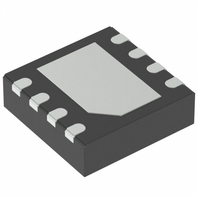
Infineon Technologies TLE72593LEXUMA1
- Part No.:
- TLE72593LEXUMA1
- Manufacturer:
- Infineon Technologies
- Category:
- Drivers, Receivers, Transceivers
- Package:
- 8-TDFN Exposed Pad
- Datasheet:
-
 TLE72593LEXUMA1.pdf
- Description:
- IC TRANSCEIVER 1/1 PGTSON81
- Quantity:
- Payment:

- Shipping:

Inventory:12,043
Please send an inquiry. Send us your inquiry, and we will respond immediately.
Product details
Overview
TLE72593LEXUMA1 from Infineon Technologies is a single-wire LIN transceiver compliant with ISO 17987-4 and LIN Specifications 2.2A, designed as the physical layer interface between automotive microcontrollers and the LIN bus. It supports data rates up to 20 kbps, operates from 5 V to 27 V supply, draws ≤8 µA in sleep mode, and features integrated wake-up via BUS or WK pin for battery-sensitive body electronics applications.
For engineers reviewing the TLE72593LEXUMA1 datasheet, TLE72593LEXUMA1 pinout, TLE72593LEXUMA1 application, or TLE72593LEXUMA1 equivalent, key selection criteria include LIN 2.2A compliance, dual-voltage logic compatibility (3.3 V/5 V), dominant time-out protection, BUS short-to-VBAT/GND handling, and AEC-Q100 qualification for under-hood and interior modules.
Technical Context
The TLE72593LEXUMA1 implements a fully integrated LIN physical layer with configurable slew-rate control-Normal Slope mode for standard communication (≤20 kbps) and Flash mode for accelerated MCU programming. Its receiver includes noise-filtering circuitry and delay symmetry optimization to improve signal integrity across temperature and voltage variations.
Mode transitions are controlled exclusively by the EN pin, with INH output enabling external regulator control and master-node bus termination switching. Wake-up detection occurs on both BUS (LIN traffic) and WK (local edge-triggered) inputs, with RxD polarity inversion signaling wake events to the host controller.
Key Specifications
| Parameter | Value and Actual Design Meaning |
|---|---|
| Bus Voltage Range | 5 V to 27 V - supports 12 V and 24 V automotive board nets without external regulation |
| Sleep Current | ≤8 µA typical - enables always-on partial-network operation with minimal battery drain |
| LIN Data Rate | Up to 20 kbps - meets LIN 2.2A timing requirements for body control and sensor networks |
| Logic Compatibility | 3.3 V and 5 V I/O - interfaces directly with common automotive MCUs without level-shifting |
| ESD Robustness | ±15 kV HBM per IEC61000-4-2 - eliminates need for external TVS in most ECU designs |
| Thermal Protection | Integrated overtemperature shutdown - prevents latch-up during sustained bus fault conditions |
| AEC-Q100 Grade | Grade 1 (−40 °C to +125 °C ambient) - qualified for engine bay and passenger compartment mounting |
Pinout & Package
Package: PG-TSON-8 (leadless, thermally enhanced, AOI-compatible), 3 mm × 3 mm, 0.65 mm pitch, exposed thermal pad.
| Pin/Terminal | Circuit Role | Design Meaning |
|---|---|---|
| RxD | Receive data output | Active-low LIN bus signal replica; requires external pull-up for wake-up indication |
| EN | Enable input | CMOS-compatible enable; internal pull-down; HIGH activates Normal/Sleep modes |
| WK | Local wake input | Edge-triggered, active-low; internal pull-up; initiates wake from Sleep/Stand-By |
| TxD | Transmit data input | CMOS-compatible; LOW drives dominant bus state; includes timeout protection |
| GND | Ground reference | Power and signal return; connected to thermal pad for thermal dissipation |
| BUS | LIN bus interface | Single-wire bidirectional I/O with internal termination and short-circuit protection |
| VS | Battery supply input | 5–27 V primary power rail; powers internal regulators and output stage |
| INH | Inhibit output | Battery-referenced open-drain output; controls external regulators or master termination |
Key Features
| Feature | Design Value |
|---|---|
| Flash Mode Slew Rate | Accelerated edge rate for fast MCU flash programming without violating LIN timing margins |
| Dominant Time-Out | Hardware-enforced TxD dominant duration limit prevents bus lock-up during firmware faults |
| BUS Short Protection | Automatic recovery from BUS-to-VBAT or BUS-to-GND shorts without latch-up or damage |
| EMC Optimized Driver | Controlled rise/fall times reduce broadband emissions while maintaining signal integrity |
| Supply Undervoltage Detection | Internal monitoring disables outputs below VS threshold to prevent undefined bus states |
Applications
| Body Control Module | Door Module |
|---|---|
Use Scenario: Centralized control of window lifters, mirrors, locks, and interior lighting in modern vehicle door assemblies. IC Role / Device Role / Timing Role: LIN physical layer transceiver interfacing MCU to distributed slave nodes (e.g., motor drivers, sensors). Use Value: Enables low-cost, low-power communication with <8 µA sleep current and ±15 kV ESD robustness in high-humidity environments. | Use Scenario: Integration of proximity sensors, anti-pinch actuators, and LED status indicators within compact door ECUs. IC Role / Device Role / Timing Role: Bus driver providing LIN 2.2A-compliant signaling with Flash mode support for field firmware updates. Use Value: Reduces BOM count via integrated BUS termination and eliminates external level shifters with 3.3 V/5 V logic compatibility. |
| Roof Module | Seat Control Unit |
Use Scenario: Coordination of sunroof motors, ambient lighting, and rain sensor signals in overhead console systems. IC Role / Device Role / Timing Role: LIN slave transceiver with local wake capability for event-driven operation (e.g., button press, light change). Use Value: Supports partial network wake-up with <10 µs response latency and low leakage on BUS pin during standby. | Use Scenario: Position memory, heating control, and lumbar adjustment in power-adjustable automotive seats. IC Role / Device Role / Timing Role: Master-mode LIN transceiver driving seat position sensors and motor drivers via daisy-chained topology. Use Value: INH output enables dynamic control of external 1 kΩ master termination resistor and 5 V LDO for MCU domain. |
Equivalent & Alternatives
The following parts are listed as comparable options for similar LIN transceiver applications.
| Alternative Part | Technical Difference | Application Difference | Selection Advice |
|---|---|---|---|
| TLIN1029DRBR | TI device with integrated 5 V LDO; no INH output; lower sleep current (3 µA) | Best suited for self-powered slave nodes where local regulation is required | Select when system-level power architecture relies on integrated LDO rather than external regulator control |
| ATA663211-GAQW | Microchip device with wake-on-data feature; higher bus voltage tolerance (40 V); no Flash mode | Preferred for 24 V commercial vehicles requiring extended overvoltage robustness | Select when operating beyond 27 V or requiring wake-on-recessive-bit detection instead of edge-triggered WK |
Compared with TLIN1029DRBR and ATA663211-GAQW, the TLE72593LEXUMA1 uniquely combines INH-controlled external power management, Flash mode for programming acceleration, and AEC-Q100 Grade 1 qualification at 125 °C ambient-making it optimal for thermally constrained master nodes in passenger car ECUs.
Availability
TLE72593LEXUMA1 is available at Aetrix Electronics and suitable for body control modules, door modules, roof consoles, and seat control units requiring stable component supply across automotive production lifecycles.
Supply support for TLE72593LEXUMA1 includes scheduled delivery planning, volume procurement assistance, BOM continuity management, traceable sourcing, and lifecycle availability coordination for OEM customers, industrial embedded developers, connected-device designers, and electronics production programs.
Manufacturer
Infineon Technologies is a German semiconductor manufacturer specializing in power management, automotive ICs, and security solutions, with global manufacturing and automotive qualification infrastructure.
The TLE72593LEXUMA1 belongs to Infineon's Smart Power Technology (SPT®) LIN transceiver family, engineered specifically for AEC-Q100-compliant automotive body electronics requiring ultra-low sleep current, high EMC immunity, and robust fault handling.
FAQ
What LIN protocol versions does the TLE72593LEXUMA1 support?
The TLE72593LEXUMA1 is compliant with LIN Specification Versions 1.2, 1.3, 2.0, 2.1, 2.2, and 2.2A, as well as ISO 17987-4. It supports all mandatory electrical characteristics-including dominant/recessive voltage thresholds, slew rate limits, and timing tolerances-across the full 2.4 kbps to 20 kbps data rate range.
How does the INH pin function in master versus slave node configurations?
In master node configuration, INH (set HIGH) enables external 1 kΩ termination resistor control and can drive an external 5 V LDO for MCU power. In slave node use, INH remains unconnected or pulled low; its primary role is regulator enablement-not bus termination-since slaves rely on master-supplied recessive bias.
Can the TLE72593LEXUMA1 operate without an external pull-up on RxD?
No. An external pull-up resistor to the MCU's logic supply (3.3 V or 5 V) is mandatory on RxD to ensure correct wake-up indication: RxD goes LOW after BUS or WK wake events, and HIGH after power-up. Without this pull-up, wake detection fails and logic levels become undefined during mode transitions.
What is the purpose of Flash Mode, and how is it activated?
Flash Mode provides faster bus edge rates to reduce programming time during MCU firmware updates over LIN. It is entered only from Normal Slope mode by asserting a specific pulse sequence on TxD (per datasheet Figure 12), not via EN or WK. The transceiver automatically reverts to Normal Slope mode after timeout or explicit command.
TLE72593LEXUMA1 Specifications
- Product attributes
- Attribute value
- Manufacturer:
- Infineon Technologies
- Series:
- -
- Package/Case:
- 8-TDFN Exposed Pad
- Packaging:
- Tape & Reel (TR)
- Product Status:
- Active
- Type:
- Transceiver
- Protocol:
- LINbus
- Number of Drivers/Receivers:
- 1/1
- Duplex:
- -
- Receiver Hysteresis:
- 120 mV
- Data Rate:
- 20kbps
- Voltage - Supply:
- 5.5V ~ 27V
- Operating Temperature:
- -40°C ~ 150°C
- Grade:
- -
- Qualification:
- -
- Mounting Type:
- Surface Mount, Wettable Flank
- Supplier Device Package:
- PG-TSON-8-1
TLE72593LEXUMA1 FAQ
1.How can I place an order for TLE72593LEXUMA1 through Aetrix?
Please submit a Request for Quotation (RFQ) for TLE72593LEXUMA1 on Aetrix. Our sales agent will provide a competitive quotation and guide you through the order confirmation once you accept the terms.
2.Are the price and stock information for TLE72593LEXUMA1 reliable?
The price and inventory of TLE72593LEXUMA1 are updated periodically and may fluctuate due to market conditions. Stock and pricing data are typically refreshed every 24 hours. Quotation validity for TLE72593LEXUMA1 is usually 5 days.
3.What payment methods are accepted for TLE72593LEXUMA1?
We accept Wire Transfer, PayPal, Credit Card, Western Union, MoneyGram, and Escrow for TLE72593LEXUMA1 transactions.
Note: Certain payment methods may incur a processing fee.
4.How is shipping managed for TLE72593LEXUMA1?
TLE72593LEXUMA1 orders can be shipped via leading logistics carriers, including DHL, UPS, FedEx, TNT, or Registered Mail.
Once your TLE72593LEXUMA1 order is processed, you will receive an email with the shipment details and tracking number.
Note: Tracking information may take up to 24 hours to appear. Express delivery typically takes 3–5 business days.
5.How can I obtain technical support or documentation for TLE72593LEXUMA1?
For technical support, including TLE72593LEXUMA1 datasheets, pinout diagrams, or application guidance, please contact our engineering support team. They can provide detailed documentation and assistance for your TLE72593LEXUMA1 requirements.
6.How does Aetrix verify that TLE72593LEXUMA1 is sourced from the original manufacturer or authorized distributors?
All TLE72593LEXUMA1 products on Aetrix are procured from qualified distributors and authorized channels. Our dedicated quality assurance team conducts strict verification, including traceability checks and, if necessary, third-party testing. This ensures that TLE72593LEXUMA1 meets industry standards.
7.What is the process for return or replacement of TLE72593LEXUMA1?
All TLE72593LEXUMA1 units undergo pre-shipment inspection (PSI). If there is an issue with TLE72593LEXUMA1, returns or replacements are accepted under the following conditions:
1.Quantity discrepancies, incorrect items, or visible external defects (such as breakage or corrosion), acknowledged by Aetrix.
2.The issue is reported within 90 days of delivery.
3.The TLE72593LEXUMA1 part is unused and in its original packaging.
Return procedure for TLE72593LEXUMA1:
1.Submit a request within 90 days.
2.Obtain a Return Material Authorization (RMA) from Aetrix.
TLE72593LEXUMA1 Tags

-
ATA6561-GAQW-N
Microchip Technology
-
ATA6561-GBQW-N
Microchip Technology

-
AM26LS32ACDR
Texas Instruments

-
SP485CN-L/TR
MaxLinear, Inc.
-
SP485EN-L/TR
MaxLinear, Inc.
-
SP485EEN-L/TR
MaxLinear, Inc.
-
SP485ECN-L/TR
MaxLinear, Inc.
-
THVD1400DR
Texas Instruments
-
AM26C31IDR
Texas Instruments

-
TLIN1021ADRQ1
Texas Instruments
-
MAX232IDR
Texas Instruments
-
AM26C32IDR
Texas Instruments
Tech Hub

18650 battery guide covering lithium-ion cell basics, 3.6V/3.7V voltage, 4.2V charging, mAh and Wh capacity, protected cells, chargers, BMS, series-parallel packs, holders, welding and sourcing checks.…

Hall effect sensor guide covering working principle, linear and digital sensors, Arduino circuits, current sensing, speed detection, automotive applications, A3144 examples, signal filtering and datash…

Product Change Notification guide for electronic components, covering PCN meaning, PCN vs PDN/EOL, common change types, risk levels, form-fit-function review, engineering validation, BOM control, LTB/L…

A practical guide to blend door actuators, covering HVAC function, symptoms, location, AC and heater issues, reset and calibration, replacement cost, electrical diagnosis, compatibility checks, and rep…

Engineering guide to Raspberry Pi alternatives, covering chip-level differences, Orange Pi, ROCK, Jetson, Banana Pi, NanoPi, Compute Module, Pico, GPIO, camera, HAT compatibility, and replacement risks…

Engineering guide to dynamic load response testing for high-current buck converters, covering load step setup, slew rate, Vcore undershoot, overshoot, recovery time, probe location, output capacitors a…

Engineering guide to output capacitor selection for ASIC Vcore rails, covering bulk capacitors, polymer capacitors, MLCC decoupling, DC bias, ESR, ESL, placement, transient response and substitution ri…

Engineering guide to high-current ASIC Vcore rails, covering 12-phase buck architecture, PMBus control, dynamic load testing, output capacitor networks, smart power stage selection, thermal design and …

Voltage regulator guide covering linear, LDO, 7805, Zener, adjustable, buck, VRM and alternator regulators, with design checks, testing methods, troubleshooting and datasheet-based selection.

Amplifier guide covering voltage, current and power amplification, gain, feedback, amplifier classes, audio and RF applications, op-amp circuits, transimpedance amplifiers, datasheet selection and trou…


