
 My Inquiry
 My Account


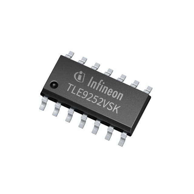
Infineon Technologies TLE9252VSKXUMA1
- Part No.:
- TLE9252VSKXUMA1
- Manufacturer:
- Infineon Technologies
- Category:
- Drivers, Receivers, Transceivers
- Package:
- 14-SOIC (0.154", 3.90mm Width)
- Datasheet:
-
 TLE9252VSKXUMA1.pdf
- Description:
- IC TRANSCEIVER HALF 1/1 PGDSO14
- Quantity:
- Payment:

- Shipping:

Inventory:8,843
Please send an inquiry. Send us your inquiry, and we will respond immediately.
Product details
Overview
TLE9252VSKXUMA1 from Infineon Technologies is a high-speed CAN FD transceiver compliant with ISO 11898-2:2016 and SAE J2284-4/-5, supporting data rates up to 5 Mbit/s. It serves as the physical layer interface between a CAN protocol controller and the HS CAN bus, featuring autonomous bus biasing, dual power supply (VBAT/VCC), and fail-safe functions including TxD time-out, RxD recessive clamping, and overtemperature shutdown.
For engineers reviewing the TLE9252VSKXUMA1 datasheet, TLE9252VSKXUMA1 pinout, TLE9252VSKXUMA1 application, or TLE9252VSKXUMA1 equivalent, key selection criteria include loop delay symmetry for CAN FD timing integrity, ±10 kV HBM ESD robustness, sleep-mode current ≤25 µA, and WUP filter time programmability (0.5–1.8 µs) for OEM-specific wake-up compliance.
Technical Context
The TLE9252VSKXUMA1 implements a fully differential transmitter/receiver architecture with matched propagation delays on CANH and CANL paths, enabling precise loop delay symmetry (<10 ns typical) critical for reliable CAN FD frame reception at 5 Mbit/s. Its mode control logic supports four operational states-Normal, Receive-only, Stand-by, and Sleep-with autonomous transitions triggered by EN, NSTB, and WAKE inputs.
It integrates dual-supply regulation (VBAT for robust cranking support, VCC for transmitter operation) and voltage-level shifting via VIO (3.3 V or 5 V compatible), while NERR provides combined failure diagnosis and wake-up status indication. The open-drain INH output enables external circuit control during low-power modes.
Key Specifications
| Parameter | Value and Actual Design Meaning |
|---|---|
| Max Data Rate | 5 Mbit/s - Enables full CAN FD payload transmission without bit stuffing limitations. |
| Sleep Current | ≤25 µA - Ensures ultra-low quiescent draw in vehicle off-state for battery-sensitive modules. |
| ESD Robustness | ±10 kV HBM / ±9 kV IEC 61000-4-2 - Protects against assembly handling and in-vehicle electrostatic events. |
| WUP Filter Time | 0.5 µs to 1.8 µs - Configurable window for standardized wake-up pattern detection across global OEMs. |
| Bus Fault Tolerance | CAN short-circuit proof to GND, battery, and VCC - Maintains functionality during wiring faults in harsh automotive environments. |
| Supply Range | VBAT: −0.3 V to 40 V; VCC/VIO: −0.3 V to 6.0 V - Supports cold-crank (down to 3 V) and load-dump (up to 40 V) conditions. |
| Thermal Shutdown | Active at >175 °C - Prevents permanent damage during sustained overtemperature operation. |
Pinout & Package
Supplied in RoHS-compliant PG-DSO-14 package (14-pin, exposed thermal pad), optimized for automotive PCB layout and thermal dissipation under under-hood conditions.
| Pin/Terminal | Circuit Role | Design Meaning |
|---|---|---|
| 1 TxD | Transmit Data Input | CMOS input with internal pull-up to VIO; drives dominant state when low. |
| 2 GND | Ground Reference | Primary return path for VCC, VIO, VBAT, and CAN signals; connects to thermal pad. |
| 3 VCC | Transmitter Supply | Provides power to driver stage; requires 100 nF decoupling to GND. |
| 4 RxD | Receive Data Output | CMOS output level-shifted to VIO; low during dominant bus state. |
| 5 VIO | Digital I/O Reference | Sets logic threshold for TxD/RxD/EN/NSTB; supports 3.3 V or 5 V microcontrollers. |
| 6 EN | Enable Control Input | Pull-down enabled; high = Normal Mode, low = Stand-by/Sleep entry. |
| 7 INH | Inhibit Output | Open-drain output to disable external regulators or LDOs during Sleep Mode. |
| 8 NERR | Error & Wake-Up Flag | Active-low output indicating fault (overtemp, undervoltage) or local/wake-up event. |
| 9 WAKE | Local Wake-Up Input | Edge-sensitive input (rising/falling); terminated between GND and VBAT for noise immunity. |
| 10 VBAT | Battery Supply | Main power rail; handles cranking (≥3 V) and load-dump (≤40 V) per ISO 16750-2. |
| 11 N.C. | No Connect | Internally unused pin; must remain unconnected on PCB. |
| 12 CANL | CAN Bus Low Line | Differential bus terminal; internally biased to VCC/2 for recessive state stability. |
| 13 CANH | CAN Bus High Line | Differential bus terminal; complements CANL with matched drive strength and delay. |
| 14 NSTB | Stand-by Control Input | Pull-down enabled; high = Normal Mode, low = Stand-by (reduced current vs. Sleep). |
Key Features
| Feature | Design Value |
|---|---|
| Autonomous Bus Biasing | Internal VCC/2 termination ensures ISO 11898-2-compliant recessive voltage levels without external resistors. |
| Chokeless Operation | Low EME due to <10 ns CANH/CANL loop delay symmetry eliminates need for common-mode choke in most layouts. |
| Dual Power Architecture | Independent VBAT (system supply) and VCC (transmitter supply) enable stable operation during battery cranking. |
| Fail-Safe Diagnostics | NERR pin reports undervoltage (VBAT/VCC/VIO), overtemperature, and TxD timeout events with distinct timing signatures. |
| Configurable WUP Detection | Filter time adjustable via external RC network on WAKE pin to meet OEM-specific wake-up latency requirements. |
Applications
| Infotainment Head Unit | Instrument Cluster Module |
|---|---|
Use Scenario: Real-time audio/video streaming and UI updates over CAN FD backbone in premium vehicle infotainment systems. IC Role / Device Role / Timing Role: Physical layer transceiver bridging MCU's CAN controller to high-bandwidth infotainment bus segment. Use Value: 5 Mbit/s capability enables sub-100 µs latency for touch response synchronization and display refresh coordination. |
Use Scenario: Aggregating speed, RPM, fuel, and ADAS warning signals for digital instrument cluster rendering. IC Role / Device Role / Timing Role: HS CAN FD interface ensuring deterministic delivery of safety-critical metrics to cluster MCU. Use Value: Guaranteed loop delay symmetry prevents bit errors in fast-changing analog-derived CAN frames during rapid acceleration/deceleration. |
| Radar Sensor Node | HVAC Control Module |
Use Scenario: Transmitting raw radar point-cloud metadata and calibration commands between 77 GHz radar ECU and domain controller. IC Role / Device Role / Timing Role: Robust CAN FD physical layer interface operating in high-EMI engine bay environment. Use Value: ±10 kV HBM ESD rating and CAN short-circuit protection ensure uninterrupted radar communication during service or fault conditions. |
Use Scenario: Coordinating cabin temperature setpoints, blower speed, and air-mix door positions across multi-zone HVAC system. IC Role / Device Role / Timing Role: Low-power CAN transceiver maintaining network presence during vehicle sleep with 25 µA quiescent current. Use Value: WUP filter time configurability allows HVAC module to respond within 1.8 µs to climate-change requests from key fob or smartphone app. |
Equivalent & Alternatives
The following parts are listed as comparable options for similar high-speed CAN FD transceiver applications.
| Alternative Part | Technical Difference | Application Difference | Selection Advice |
|---|---|---|---|
| TCAN1042VDQ1 | Single-supply (VCC only); no VBAT rail; lower ESD (±7 kV HBM); fixed 1.2 µs WUP filter. | Lacks battery-cranking resilience; unsuitable for direct VBAT connection in body control modules. | Preferred where cost-sensitive designs use regulated 5 V supply and OEM WUP timing is fixed. |
| ADM3053BRWZ | Integrated isolated DC/DC converter; no VIO level shift; higher sleep current (60 µA); no NERR diagnostic pin. | Designed for galvanically isolated networks; adds BOM cost and board area vs. non-isolated use cases. | Select when ground-loop elimination or high-voltage barrier (>2.5 kV RMS) is mandatory in EV powertrain subsystems. |
Compared with TCAN1042VDQ1 and ADM3053BRWZ, the TLE9252VSKXUMA1 uniquely combines VBAT cranking tolerance, configurable WUP timing, and integrated NERR diagnostics-making it optimal for AEC-Q100-compliant body electronics requiring both ultra-low sleep current and OEM-specific wake-up compliance.
Availability
TLE9252VSKXUMA1 is available at Aetrix Electronics and suitable for infotainment head units, instrument cluster modules, radar sensor nodes, and HVAC control modules requiring stable component supply across automotive production lifecycles.
Supply support for TLE9252VSKXUMA1 includes scheduled delivery planning, volume procurement assistance, BOM continuity management, traceable sourcing, and lifecycle availability coordination for OEM customers, industrial embedded developers, connected-device designers, and electronics production programs.
Manufacturer
Infineon Technologies is a German semiconductor manufacturer specializing in power management, automotive ICs, and security solutions, with global manufacturing and automotive qualification infrastructure.
The TLE9252VSKXUMA1 belongs to Infineon's automotive transceiver product line, engineered specifically for high-reliability CAN FD communication in ASIL-B–capable ECUs under extended temperature (−40 °C to 150 °C) and voltage stress conditions.
FAQ
What is the maximum CAN FD data rate supported by the TLE9252VSKXUMA1?
The TLE9252VSKXUMA1 supports up to 5 Mbit/s, verified per ISO 11898-2:2016 Annex D test procedures. This rate is achievable with guaranteed loop delay symmetry <10 ns and matched CANH/CANL rise/fall times, enabling error-free transmission of CAN FD frames with 64-byte payloads in automotive networks.
How does the TLE9252VSKXUMA1 handle battery cranking conditions?
It uses a dual-supply architecture: VBAT (−0.3 V to 40 V) powers internal biasing and wake-up circuitry, while VCC (−0.3 V to 6.0 V) supplies the transmitter. During cranking (VBAT down to ~3 V), the device remains functional in Normal or Stand-by Mode, and retains Sleep Mode wake-up capability via WAKE pin.
Is the TLE9252VSKXUMA1 pin-compatible with earlier Infineon CAN transceivers like TLE6250?
No. The TLE9252VSKXUMA1 has 14 pins and distinct pin assignments (e.g., separate VBAT, VIO, INH, NERR, WAKE), whereas TLE6250 is an 8-pin device with different mode control and diagnostic signaling. Migration requires PCB layout revision and firmware adaptation for new pin functions and timing behavior.
What diagnostic capabilities does the NERR pin provide?
NERR is an active-low, open-drain output that indicates undervoltage (on VBAT, VCC, or VIO), overtemperature shutdown, TxD time-out, or local/wake-up events. Its pulse width and timing distinguish fault types per datasheet Table 12, enabling MCU-based root-cause analysis without additional sensors.
TLE9252VSKXUMA1 Specifications
- Product attributes
- Attribute value
- Manufacturer:
- Infineon Technologies
- Series:
- -
- Package/Case:
- 14-SOIC (0.154", 3.90mm Width)
- Packaging:
- Tape & Reel (TR)
- Product Status:
- Active
- Type:
- Transceiver
- Protocol:
- CANbus
- Number of Drivers/Receivers:
- 1/1
- Duplex:
- Half
- Receiver Hysteresis:
- 30 mV
- Data Rate:
- 5Mbps
- Voltage - Supply:
- 4.5V ~ 5.5V
- Operating Temperature:
- -40°C ~ 150°C (TJ)
- Grade:
- Automotive
- Qualification:
- AEC-Q100
- Mounting Type:
- Surface Mount
- Supplier Device Package:
- PG-DSO-14
TLE9252VSKXUMA1 FAQ
1.How can I place an order for TLE9252VSKXUMA1 through Aetrix?
Please submit a Request for Quotation (RFQ) for TLE9252VSKXUMA1 on Aetrix. Our sales agent will provide a competitive quotation and guide you through the order confirmation once you accept the terms.
2.Are the price and stock information for TLE9252VSKXUMA1 reliable?
The price and inventory of TLE9252VSKXUMA1 are updated periodically and may fluctuate due to market conditions. Stock and pricing data are typically refreshed every 24 hours. Quotation validity for TLE9252VSKXUMA1 is usually 5 days.
3.What payment methods are accepted for TLE9252VSKXUMA1?
We accept Wire Transfer, PayPal, Credit Card, Western Union, MoneyGram, and Escrow for TLE9252VSKXUMA1 transactions.
Note: Certain payment methods may incur a processing fee.
4.How is shipping managed for TLE9252VSKXUMA1?
TLE9252VSKXUMA1 orders can be shipped via leading logistics carriers, including DHL, UPS, FedEx, TNT, or Registered Mail.
Once your TLE9252VSKXUMA1 order is processed, you will receive an email with the shipment details and tracking number.
Note: Tracking information may take up to 24 hours to appear. Express delivery typically takes 3–5 business days.
5.How can I obtain technical support or documentation for TLE9252VSKXUMA1?
For technical support, including TLE9252VSKXUMA1 datasheets, pinout diagrams, or application guidance, please contact our engineering support team. They can provide detailed documentation and assistance for your TLE9252VSKXUMA1 requirements.
6.How does Aetrix verify that TLE9252VSKXUMA1 is sourced from the original manufacturer or authorized distributors?
All TLE9252VSKXUMA1 products on Aetrix are procured from qualified distributors and authorized channels. Our dedicated quality assurance team conducts strict verification, including traceability checks and, if necessary, third-party testing. This ensures that TLE9252VSKXUMA1 meets industry standards.
7.What is the process for return or replacement of TLE9252VSKXUMA1?
All TLE9252VSKXUMA1 units undergo pre-shipment inspection (PSI). If there is an issue with TLE9252VSKXUMA1, returns or replacements are accepted under the following conditions:
1.Quantity discrepancies, incorrect items, or visible external defects (such as breakage or corrosion), acknowledged by Aetrix.
2.The issue is reported within 90 days of delivery.
3.The TLE9252VSKXUMA1 part is unused and in its original packaging.
Return procedure for TLE9252VSKXUMA1:
1.Submit a request within 90 days.
2.Obtain a Return Material Authorization (RMA) from Aetrix.
TLE9252VSKXUMA1 Tags

-
ATA6561-GAQW-N
Microchip Technology
-
ATA6561-GBQW-N
Microchip Technology

-
AM26LS32ACDR
Texas Instruments

-
SP485CN-L/TR
MaxLinear, Inc.
-
SP485EN-L/TR
MaxLinear, Inc.
-
SP485EEN-L/TR
MaxLinear, Inc.
-
SP485ECN-L/TR
MaxLinear, Inc.
-
THVD1400DR
Texas Instruments
-
AM26C31IDR
Texas Instruments

-
TLIN1021ADRQ1
Texas Instruments
-
MAX232IDR
Texas Instruments
-
AM26C32IDR
Texas Instruments
Tech Hub

18650 battery guide covering lithium-ion cell basics, 3.6V/3.7V voltage, 4.2V charging, mAh and Wh capacity, protected cells, chargers, BMS, series-parallel packs, holders, welding and sourcing checks.…

Hall effect sensor guide covering working principle, linear and digital sensors, Arduino circuits, current sensing, speed detection, automotive applications, A3144 examples, signal filtering and datash…

Product Change Notification guide for electronic components, covering PCN meaning, PCN vs PDN/EOL, common change types, risk levels, form-fit-function review, engineering validation, BOM control, LTB/L…

A practical guide to blend door actuators, covering HVAC function, symptoms, location, AC and heater issues, reset and calibration, replacement cost, electrical diagnosis, compatibility checks, and rep…

Engineering guide to Raspberry Pi alternatives, covering chip-level differences, Orange Pi, ROCK, Jetson, Banana Pi, NanoPi, Compute Module, Pico, GPIO, camera, HAT compatibility, and replacement risks…

Engineering guide to dynamic load response testing for high-current buck converters, covering load step setup, slew rate, Vcore undershoot, overshoot, recovery time, probe location, output capacitors a…

Engineering guide to output capacitor selection for ASIC Vcore rails, covering bulk capacitors, polymer capacitors, MLCC decoupling, DC bias, ESR, ESL, placement, transient response and substitution ri…

Engineering guide to high-current ASIC Vcore rails, covering 12-phase buck architecture, PMBus control, dynamic load testing, output capacitor networks, smart power stage selection, thermal design and …

Voltage regulator guide covering linear, LDO, 7805, Zener, adjustable, buck, VRM and alternator regulators, with design checks, testing methods, troubleshooting and datasheet-based selection.

Amplifier guide covering voltage, current and power amplification, gain, feedback, amplifier classes, audio and RF applications, op-amp circuits, transimpedance amplifiers, datasheet selection and trou…


