
 My Inquiry
 My Account


Infineon Technologies XC8662FRABEFXUMA1
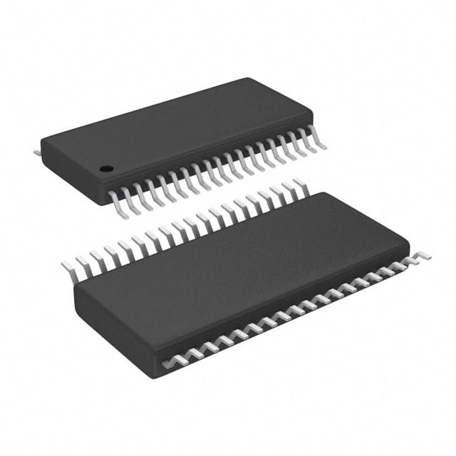
- Part No.:
- XC8662FRABEFXUMA1
- Manufacturer:
- Infineon Technologies
- Category:
- Microcontrollers
- Package:
- 38-TFSOP (0.173", 4.40mm Width)
- Datasheet:
-
 XC8662FRABEFXUMA1.pdf
- Description:
- IC MCU 8BIT 8KB FLASH 38TSSOP
- Quantity:
- Payment:

- Shipping:

Inventory:3,808
Please send an inquiry. Send us your inquiry, and we will respond immediately.
Product details
Overview
XC8662FRABEFXUMA1 from Infineon Technologies is an 8-bit single-chip microcontroller based on the XC800 core, compatible with the standard 8051 instruction set and executing instructions at two clocks per machine cycle. It integrates 4 Kbytes of Flash program memory, 512 bytes of XRAM, 256 bytes of RAM, and 8 Kbytes of Boot ROM with on-chip debug monitor. It operates with 5.0 V I/O supply and 2.5 V core logic supply (internally regulated), and targets automotive motor control and body electronics applications.
For engineers reviewing the XC8662FRABEFXUMA1 datasheet, XC8662FRABEFXUMA1 pinout, XC8662FRABEFXUMA1 application, or XC8662FRABEFXUMA1 equivalent, key selection criteria include its 10-bit 8-channel ADC resolution, CCU6 capture/compare unit for PWM generation, UART/SSC serial interfaces, watchdog timer configurability, and PG-TSSOP-38 package compatibility with automotive-grade thermal range (–40 °C to 125 °C).
Technical Context
The XC8662FRABEFXUMA1 implements a two-clock-per-cycle 8051-compatible core with dual data pointers and integrated voltage regulation delivering 2.5 V to the core from a 5.0 V supply. Its memory architecture separates 4 Kbytes of P-Flash (program) and 4 Kbytes of D-Flash (data), both supporting memory protection via PASSWD register access control and page-based addressing with rwh (read/write/hardware) access type.
Peripheral integration includes three 16-bit timers (T0/T1/T2), a dedicated 16-bit CCU6 unit for high-resolution PWM and dead-time insertion, a full-duplex UART, synchronous serial channel (SSC), and an 8-channel 10-bit SAR ADC with configurable sampling timing and reference selection. Reset sources include power-on, brownout (core supply), watchdog, and external interrupt wake-up from power-down mode.
Key Specifications
| Parameter | Value and Actual Design Meaning |
|---|---|
| Core Architecture | XC800 8-bit CPU, 8051-compatible, 2-clock/machine cycle for zero-wait-state execution |
| Flash Memory | 4 Kbytes P-Flash + 4 Kbytes D-Flash; supports in-system programming and memory protection |
| ADC Resolution | 10-bit SAR with 8 input channels; enables precise analog sensing in motor current or temperature feedback loops |
| CCU6 Unit | 16-bit capture/compare unit with 3 independent PWM channels and programmable dead-time control |
| Supply Voltages | 5.0 V I/O supply (VDD/VDDP); 2.5 V core logic (internally regulated); supports automotive battery rail operation |
| Operating Temperature | –40 °C to +125 °C (SAK grade); qualified for under-hood automotive environments |
| Package | PG-TSSOP-38; 0.65 mm pitch, surface-mount, thermally enhanced for compact motor drive PCBs |
Pinout & Package
XC8662FRABEFXUMA1 is housed in a 38-pin PG-TSSOP (Plastic Thin Shrink Small Outline Package) with exposed thermal pad, optimized for thermal dissipation in motor control modules. Pin functions are defined per the XC866 datasheet revision V1.2 (2007), with dedicated pins for CCU6 outputs, ADC inputs, UART/SSC signals, and reset/wake-up triggers.
| Pin/Terminal | Circuit Role | Design Meaning |
|---|---|---|
| VDD, VDDP | Digital I/O power supply | 5.0 V supply for port drivers and peripheral I/O; decoupling required per datasheet layout guidelines |
| VSS | Digital ground reference | Common return path for digital logic and I/O circuits; separate from analog ground in mixed-signal layout |
| VAREF | ADC reference voltage input | Accepts external reference (0–5 V) or internal 2.5 V bandgap; sets full-scale range for 10-bit conversion |
| CC60–CC62 | CCU6 PWM output terminals | Three complementary PWM outputs with dead-time programmability; directly drive gate drivers in 3-phase inverters |
| AD0–AD7 | ADC analog input channels | Eight multiplexed inputs supporting single-ended or differential acquisition; used for current sensing and temperature monitoring |
| RXD/TXD | UART serial interface | Full-duplex asynchronous communication; supports LIN physical layer via software bit-banging or external transceiver |
Key Features
| Feature | Design Value |
|---|---|
| On-chip voltage regulator | Generates stable 2.5 V core supply from 5.0 V rail, eliminating need for external LDO in cost-sensitive automotive modules |
| Memory protection scheme | Register-level password (PASSWD.PASS) and page-access control prevent unauthorized flash modification during field updates |
| Power-down wake-up capability | Interrupt-driven wake-up from power-down mode via RXD pin or EXINT0, enabling ultra-low-power sleep states in body control units |
| Boot ROM with monitor | 8 Kbytes including 1 Kbyte debug monitor ROM and 64 bytes monitor RAM for in-circuit debugging without external emulator |
| CCU6 dead-time insertion | Programmable dead-time (1–64 clock cycles) between complementary PWM outputs prevents shoot-through in half-bridge drivers |
Applications
| Automotive Fan Control | BLDC Motor Starter |
|---|---|
|
Use Scenario: Closed-loop speed regulation of radiator cooling fans using PWM-driven 12 V DC motors. IC Role / Device Role / Timing Role: MCU executes PID algorithm, reads tachometer signal via GPIO capture, and generates phase-aligned PWM via CCU6. Use Value: Integrated 10-bit ADC measures motor current for overcurrent protection; CCU6 dead-time prevents MOSFET short-circuit during commutation. |
Use Scenario: Sensorless startup and commutation sequencing for brushless DC motors in power seat actuators. IC Role / Device Role / Timing Role: MCU samples back-EMF via ADC channels, calculates rotor position, and triggers six-step commutation using CCU6 PWM outputs. Use Value: Dual data pointers accelerate real-time vector math; 2.5 V core ensures stable timing across battery voltage fluctuations (9–16 V). |
| Body Control Module (BCM) | Window Lift Controller |
|
Use Scenario: Centralized management of door locks, interior lighting, and mirror adjustment in entry systems. IC Role / Device Role / Timing Role: MCU acts as system coordinator, polling switches via GPIO, driving relays/LEDs, and communicating via UART to gateway ECU. Use Value: 4 Kbytes Flash accommodates LIN protocol stack and diagnostics; power-down wake-up on RXD enables low-quiescent-current standby mode. |
Use Scenario: Anti-pinch detection and soft-stop control for automotive power windows using current profiling. IC Role / Device Role / Timing Role: MCU monitors motor current via ADC, detects stall conditions, and reverses direction using CCU6-complementary PWM outputs. Use Value: On-chip 256-byte RAM stores real-time current history; watchdog timer ensures fail-safe shutdown if control loop hangs. |
Equivalent & Alternatives
The following parts are listed as comparable options for similar 8-bit automotive microcontroller applications.
| Alternative Part | Technical Difference | Application Difference | Selection Advice |
|---|---|---|---|
| XC886L2FRA | Enhanced XC800 derivative with 8 Kbytes Flash, CAN 2.0B controller, and extended temperature support (–40 to 150 °C) | Required for CAN-based body networks; adds protocol handling overhead but eliminates external CAN transceiver | Select when CAN bus integration is mandatory and higher Flash density supports complex diagnostics |
| SAK-TC1766-512F133HR BA | TriCore 32-bit MCU with 512 Kbytes Flash, DSP extensions, and hardware FPU; significantly higher performance and code density | Suitable for advanced motor control (FOC), real-time safety monitoring, and multi-axis coordination | Choose for next-generation platforms requiring ASIL-B compliance and scalable software architecture |
Compared with XC8662FRABEFXUMA1, the XC886L2FRA adds CAN and higher Flash but increases BOM cost and design complexity, while the TC1766 delivers orders-of-magnitude compute headroom at higher power and footprint-making the XC866 optimal for cost-constrained, functionally focused automotive subsystems.
Availability
XC8662FRABEFXUMA1 is available at Aetrix Electronics and suitable for automotive fan control, BLDC motor starter, body control module, and window lift controller applications requiring stable component supply across extended temperature ranges and long production lifecycles.
Supply support for XC8662FRABEFXUMA1 includes scheduled delivery planning, volume procurement assistance, BOM continuity management, traceable sourcing, and lifecycle availability coordination for OEM customers, industrial embedded developers, connected-device designers, and electronics production programs.
Manufacturer
Infineon Technologies AG is a German semiconductor manufacturer specializing in power management, automotive ICs, and security solutions, with global R&D and manufacturing infrastructure.
The XC866 belongs to the XC800 family, designed specifically for cost-optimized automotive body and powertrain applications where 8-bit performance, robustness, and integrated peripherals like CCU6 and LIN-capable UART meet functional safety and thermal requirements.
FAQ
Does XC8662FRABEFXUMA1 support LIN physical layer communication?
No, the XC8662FRABEFXUMA1 does not integrate a LIN transceiver. However, its UART supports LIN 2.1 protocol implementation via software bit-banging or external LIN transceivers such as TLE7259-3GE. The device provides necessary timing accuracy and GPIO flexibility for reliable LIN frame generation and reception.
What is the maximum operating frequency of the XC8662FRABEFXUMA1 core?
The XC8662FRABEFXUMA1 core runs at up to 26.67 MHz with a 13.33 MHz crystal input and PLL multiplication (×2). This yields a 2-clock-per-cycle execution speed of 13.33 million instructions per second (MIPS), confirmed in Section 3.1 of the V1.2 datasheet.
Is the 4 Kbytes of D-Flash electrically erasable and reprogrammable in-circuit?
Yes, the 4 Kbytes of D-Flash is fully in-system programmable (ISP) and supports byte/word erase and write operations during application runtime. It uses the same Flash controller and protection mechanism as P-Flash, with dedicated command sequences defined in the "Flash Programming" section of the datasheet.
How is the CCU6 unit synchronized with the ADC for motor current sampling?
The CCU6 includes trigger outputs (e.g., CC60SR0) that can be configured to generate precise timing events aligned with PWM center points or edges. These signals directly initiate ADC conversions via the ADC's external trigger input, ensuring deterministic sampling of motor phase currents at optimal commutation intervals.
XC8662FRABEFXUMA1 Specifications
- Product attributes
- Attribute value
- Manufacturer:
- Infineon Technologies
- Package/Case:
- 38-TFSOP (0.173", 4.40mm Width)
- Series:
- XC8xx
- Packaging:
- Tape & Reel (TR)
- Product Status:
- Discontinued at Digi-Key
- Programmable:
- Not Verified
- Core Processor:
- XC800
- Core Size:
- 8-Bit
- Speed:
- 86MHz
- Connectivity:
- SSI, UART/USART
- Peripherals:
- Brown-out Detect/Reset, POR, PWM, WDT
- Number of I/O:
- 19
- Program Memory Size:
- 8KB (8K x 8)
- Program Memory Type:
- FLASH
- EEPROM Size:
- -
- RAM Size:
- 768 x 8
- Voltage - Supply (Vcc/Vdd):
- 4.5V ~ 5.5V
- Data Converters:
- A/D 8x10b
- Oscillator Type:
- Internal
- Operating Temperature:
- -40°C ~ 85°C (TA)
- Grade:
- -
- Qualification:
- -
- Mounting Type:
- Surface Mount
- Supplier Device Package:
XC8662FRABEFXUMA1 FAQ
1.How can I place an order for XC8662FRABEFXUMA1 through Aetrix?
Please submit a Request for Quotation (RFQ) for XC8662FRABEFXUMA1 on Aetrix. Our sales agent will provide a competitive quotation and guide you through the order confirmation once you accept the terms.
2.Are the price and stock information for XC8662FRABEFXUMA1 reliable?
The price and inventory of XC8662FRABEFXUMA1 are updated periodically and may fluctuate due to market conditions. Stock and pricing data are typically refreshed every 24 hours. Quotation validity for XC8662FRABEFXUMA1 is usually 5 days.
3.What payment methods are accepted for XC8662FRABEFXUMA1?
We accept Wire Transfer, PayPal, Credit Card, Western Union, MoneyGram, and Escrow for XC8662FRABEFXUMA1 transactions.
Note: Certain payment methods may incur a processing fee.
4.How is shipping managed for XC8662FRABEFXUMA1?
XC8662FRABEFXUMA1 orders can be shipped via leading logistics carriers, including DHL, UPS, FedEx, TNT, or Registered Mail.
Once your XC8662FRABEFXUMA1 order is processed, you will receive an email with the shipment details and tracking number.
Note: Tracking information may take up to 24 hours to appear. Express delivery typically takes 3–5 business days.
5.How can I obtain technical support or documentation for XC8662FRABEFXUMA1?
For technical support, including XC8662FRABEFXUMA1 datasheets, pinout diagrams, or application guidance, please contact our engineering support team. They can provide detailed documentation and assistance for your XC8662FRABEFXUMA1 requirements.
6.How does Aetrix verify that XC8662FRABEFXUMA1 is sourced from the original manufacturer or authorized distributors?
All XC8662FRABEFXUMA1 products on Aetrix are procured from qualified distributors and authorized channels. Our dedicated quality assurance team conducts strict verification, including traceability checks and, if necessary, third-party testing. This ensures that XC8662FRABEFXUMA1 meets industry standards.
7.What is the process for return or replacement of XC8662FRABEFXUMA1?
All XC8662FRABEFXUMA1 units undergo pre-shipment inspection (PSI). If there is an issue with XC8662FRABEFXUMA1, returns or replacements are accepted under the following conditions:
1.Quantity discrepancies, incorrect items, or visible external defects (such as breakage or corrosion), acknowledged by Aetrix.
2.The issue is reported within 90 days of delivery.
3.The XC8662FRABEFXUMA1 part is unused and in its original packaging.
Return procedure for XC8662FRABEFXUMA1:
1.Submit a request within 90 days.
2.Obtain a Return Material Authorization (RMA) from Aetrix.
XC8662FRABEFXUMA1 Tags

-
ATTINY4-TSHR
Microchip Technology
-
ATTINY10-TSHR
Microchip Technology
-
ATTINY10-TS8R
Microchip Technology

-
ATTINY202-SSNR
Microchip Technology
-
ATTINY202-SSFR
Microchip Technology
-
ATTINY402-SSNR
Microchip Technology

-
PIC16F15213T-I/MF
Microchip Technology
-
PIC16F15213-E/MF
Microchip Technology

-
PIC10F200T-I/OT
Microchip Technology
-
ATTINY412-SSNR
Microchip Technology
-
PIC10F202T-I/OT
Microchip Technology

-
ATTINY404-SSNR
Microchip Technology
Tech Hub

Guide to electronic component obsolescence covering EOL risk, PCN/PDN notices, last-time buy planning, replacement options, form-fit-function validation, counterfeit risk and BOM lifecycle management.

18650 battery guide covering lithium-ion cell basics, 3.6V/3.7V voltage, 4.2V charging, mAh and Wh capacity, protected cells, chargers, BMS, series-parallel packs, holders, welding and sourcing checks.…

Hall effect sensor guide covering working principle, linear and digital sensors, Arduino circuits, current sensing, speed detection, automotive applications, A3144 examples, signal filtering and datash…

Product Change Notification guide for electronic components, covering PCN meaning, PCN vs PDN/EOL, common change types, risk levels, form-fit-function review, engineering validation, BOM control, LTB/L…

A practical guide to blend door actuators, covering HVAC function, symptoms, location, AC and heater issues, reset and calibration, replacement cost, electrical diagnosis, compatibility checks, and rep…

Engineering guide to Raspberry Pi alternatives, covering chip-level differences, Orange Pi, ROCK, Jetson, Banana Pi, NanoPi, Compute Module, Pico, GPIO, camera, HAT compatibility, and replacement risks…

Engineering guide to dynamic load response testing for high-current buck converters, covering load step setup, slew rate, Vcore undershoot, overshoot, recovery time, probe location, output capacitors a…

Engineering guide to output capacitor selection for ASIC Vcore rails, covering bulk capacitors, polymer capacitors, MLCC decoupling, DC bias, ESR, ESL, placement, transient response and substitution ri…

Engineering guide to high-current ASIC Vcore rails, covering 12-phase buck architecture, PMBus control, dynamic load testing, output capacitor networks, smart power stage selection, thermal design and …

Voltage regulator guide covering linear, LDO, 7805, Zener, adjustable, buck, VRM and alternator regulators, with design checks, testing methods, troubleshooting and datasheet-based selection.


