
 My Inquiry
 My Account


Infineon Technologies XE164F96F66LACFXUMA1
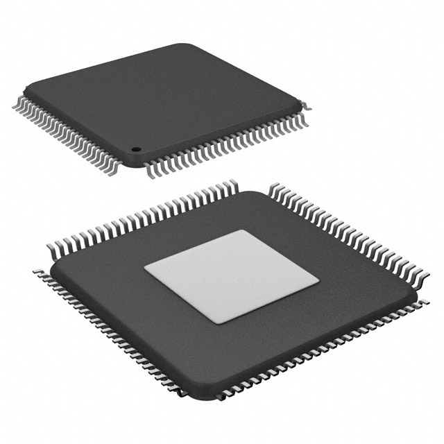
- Part No.:
- XE164F96F66LACFXUMA1
- Manufacturer:
- Infineon Technologies
- Category:
- Microcontrollers
- Package:
- 100-LQFP Exposed Pad
- Datasheet:
-
 XE164F96F66LACFXUMA1.pdf
- Description:
- IC MCU 16BIT 768KB FLASH 100LQFP
- Quantity:
- Payment:

- Shipping:

Inventory:2,852
Please send an inquiry. Send us your inquiry, and we will respond immediately.
Product details
Overview
XE164F96F66LACFXUMA1 from Infineon Technologies is a 16-bit real-time signal controller featuring an 80 MHz CPU, 768 KB on-chip Flash, 64 KB PSRAM, dual A/D converters (11+5 channels, 10-bit, <1 µs conversion), and MultiCAN interface with 4 nodes and 128 message objects. It targets motor control, industrial automation, and power electronics where deterministic timing, high-resolution PWM, and CAN-based system coordination are required.
For engineers reviewing the XE164F96F66LACFXUMA1 datasheet, XE164F96F66LACFXUMA1 pinout, XE164F96F66LACFXUMA1 application, or XE164F96F66LACFXUMA1 equivalent, key selection criteria include its 80 MHz real-time execution capability, integrated CCU6x PWM units for three-phase inverter control, dual 10-bit ADCs with hardware preprocessing, and full CAN 2.0B support across four independent nodes.
Technical Context
The XE164F96F66LACFXUMA1 implements a five-stage pipelined C166S-V2 core with zero-cycle jumps, 1-cycle MAC, and fast context switching via dual local register banks. Its memory subsystem includes 768 KB Flash (with ECC), 64 KB PSRAM, 16 KB DSRAM, 2 KB DPRAM, and 1 KB SBRAM - all mapped within a unified 16 MB linear address space.
Peripheral integration centers on real-time signal processing: two synchronizable 10-bit ADCs (16 total channels, hardware range check/data reduction), three CCU6x units for independent 3-phase PWM generation, CAPCOM2 for general-purpose capture/compare, GPT12E timers, and a MultiCAN module supporting up to 4 CAN nodes with gateway functionality and 128 message objects.
Key Specifications
| Parameter | Value and Actual Design Meaning |
|---|---|
| CPU Core | C166S-V2 16-bit RISC core with five-stage pipeline and zero-cycle jump execution |
| Max Clock Frequency | 80 MHz - enables 12.5 ns instruction cycle time for deterministic real-time response |
| Flash Memory | 768 KB on-chip Flash with ECC - supports robust firmware storage and field updates |
| ADC Resolution & Speed | 10-bit resolution, sub-1 µs conversion time per sample - suitable for fast current/voltage sampling in motor drives |
| PWM Units | Three CCU6x modules - provide independent, phase-shifted 3-phase PWM outputs with dead-time control |
| CAN Interface | MultiCAN Rev. 2.0B with 4 nodes and 128 message objects - enables distributed control network with gateway routing |
| I/O Count | Up to 75 general-purpose I/O lines - configurable as digital, analog, or peripheral function pins |
| Supply Voltage | 3.0 V to 5.5 V single supply - simplifies power design in industrial environments with wide input ranges |
Pinout & Package
XE164F96F66LACFXUMA1 is housed in a 100-pin Green LQFP package (14 mm × 14 mm, 0.5 mm pitch) with exposed thermal pad. Pin functions are defined across multiple voltage domains (M, P, I/O), including dedicated XTAL1/XTAL2 inputs for crystal oscillator operation, JTAG debug interface pins (TCK, TMS, TDI, TDO, TRST), and grouped peripheral signals for CAN, USIC, ADC, and CCU6x.
| Pin/Terminal | Circuit Role | Design Meaning |
|---|---|---|
| XTAL1 / XTAL2 | Clock Input / Output | Drive external crystal (1–20 MHz) for precise system clock generation via on-chip PLL |
| TCK / TMS / TDI / TDO / TRST | JTAG Debug Interface | Enable non-intrusive on-chip debugging, flash programming, and boundary scan testing |
| CAN0_TX / CAN0_RX | CAN Node 0 Transceiver Interface | Direct connection to external CAN transceiver for node 0 communication (Rev. 2.0B active) |
| ADCTRIG0 / ADCTRIG1 | ADC Trigger Inputs | Synchronize ADC conversions with PWM events or timer overflows for precise sampling alignment |
| CC60SR0 / CC60SR1 | CCU60 Shadow Register Outputs | Provide synchronized PWM output enable/disable control with minimal jitter for inverter gate drivers |
| VDDP / VSSP | I/O Power Supply / Ground | Separate 3.3 V or 5 V domain for port pins - isolates digital I/O noise from core logic |
Key Features
| Feature | Design Value |
|---|---|
| Dual Synchronizable 10-bit ADCs | 16 total channels (11+5), hardware data preprocessing (range check, averaging) reduces CPU load during motor current sensing |
| Three CCU6x PWM Units | Independent 3-phase center-aligned PWM generation with programmable dead-time insertion and fault protection inputs |
| MultiCAN with Gateway Mode | Route messages between up to 4 CAN networks - enables hierarchical control architectures without external bridge ICs |
| Peripheral Event Controller (PEC) | Eight-channel DMA-like transfer engine with 24-bit addressing - moves ADC results or PWM data without CPU intervention |
| On-Chip Bootloader | UART- or CAN-based firmware update capability - supports field upgrades without JTAG hardware |
| Real-Time Clock (RTC) | Independent 32.768 kHz oscillator domain with calendar functions - maintains timekeeping during low-power sleep modes |
Applications
| Industrial Motor Drive | Automotive Body Control Module |
|---|---|
|
Use Scenario: Closed-loop vector control of 3-phase AC induction or PMSM motors in HVAC compressors and industrial pumps. IC Role / Device Role / Timing Role: Real-time signal controller executing FOC algorithm, generating synchronized PWM, sampling phase currents via dual ADCs, and managing CAN-based command interface. Use Value: Sub-1 µs ADC conversion and CCU6x dead-time control ensure precise torque regulation and inverter safety compliance (IEC 61800-5-1). |
Use Scenario: Centralized body electronics unit coordinating door locks, window lifts, lighting, and mirror controls in mid-tier vehicles. IC Role / Device Role / Timing Role: CAN network master with gateway functionality, managing message routing between powertrain, comfort, and infotainment domains. Use Value: 4-node MultiCAN and 128 message objects allow concurrent handling of UDS diagnostics, LIN sub-bus bridging, and real-time actuator commands. |
| Renewable Energy Inverter | Programmable Logic Controller (PLC) I/O Module |
|
Use Scenario: Grid-tied solar inverter requiring MPPT tracking, DC-link voltage regulation, and anti-islanding detection. IC Role / Device Role / Timing Role: High-speed signal processor sampling DC/AC voltages/currents, generating isolated gate drive signals, and communicating grid status via CANopen. Use Value: 80 MHz deterministic execution and hardware ADC preprocessing enable 20 kHz switching frequency control with <2 µs loop latency. |
Use Scenario: Modular PLC base unit aggregating digital I/O, analog inputs, and fieldbus interfaces for factory automation. IC Role / Device Role / Timing Role: Central controller managing cyclic I/O scanning, motion profiling, and EtherCAT/CANopen protocol stacks. Use Value: Unified 16 MB address space and PEC-assisted data movement simplify deterministic I/O mapping and reduce jitter in 1 ms control cycles. |
Equivalent & Alternatives
The following parts are listed as comparable options for similar real-time signal controller applications.
| Alternative Part | Technical Difference | Application Difference | Selection Advice |
|---|---|---|---|
| SAF-XE164G96F66LACFXUMA1 | Same Flash/PSRAM but only 2 CAN nodes and 4 serial channels; lacks CCU62 unit | Reduced multi-network connectivity; insufficient for 4-node CAN gateway or triple 3-phase PWM systems | Select when cost optimization is critical and system requires ≤2 CAN domains and no third CCU6x PWM bank |
| SAF-XE164H96F66LACFXUMA1 | 768 KB Flash, 64 KB PSRAM, same CPU/peripherals but no MultiCAN module | No native CAN support - requires external CAN transceiver + protocol stack overhead | Choose only if application relies exclusively on UART/LIN/SPI and must avoid CAN licensing or EMI constraints |
Compared with XE164G96F66LACFXUMA1 and XE164H96F66LACFXUMA1, the XE164F96F66LACFXUMA1 uniquely delivers full 4-node MultiCAN with gateway plus three CCU6x units - making it the only variant capable of standalone implementation of complex distributed motor control systems without external co-processors or bridge ICs.
Availability
XE164F96F66LACFXUMA1 is available at Aetrix Electronics and suitable for industrial motor drives, renewable energy inverters, and automotive body control modules requiring stable component supply and long-term production continuity.
Supply support for XE164F96F66LACFXUMA1 includes scheduled delivery planning, volume procurement assistance, BOM continuity management, traceable sourcing, and lifecycle availability coordination for OEM customers, industrial embedded developers, connected-device designers, and electronics production programs.
Manufacturer
Infineon Technologies AG is a German semiconductor manufacturer specializing in power management, automotive microcontrollers, and security solutions, with global R&D and manufacturing infrastructure.
The XE164 family belongs to Infineon's real-time signal controller product line, designed specifically for deterministic control of power electronics, motor drives, and industrial automation systems requiring tight integration of analog acquisition, PWM generation, and multi-network communication.
FAQ
What is the maximum operating frequency and associated instruction cycle time?
The XE164F96F66LACFXUMA1 operates at a maximum CPU clock frequency of 80 MHz, delivering a 12.5 ns instruction cycle time. This timing is achieved using the on-chip PLL with external crystal or clock input, and applies to single-cycle instructions including 16×16 multiply and 32-bit add/subtract operations.
Does this device support hardware-accelerated motor control functions?
Yes - it integrates three CCU6x units for independent 3-phase PWM generation with programmable dead-time, fault blanking, and synchronization triggers; dual 10-bit ADCs with hardware range checking and data reduction; and a Peripheral Event Controller for automatic ADC-to-PWM data transfer without CPU involvement.
How many CAN nodes and message objects does the MultiCAN module support?
The MultiCAN module supports up to 4 independent CAN nodes with a total of 128 configurable message objects. Each node operates under CAN 2.0B protocol with full acceptance filtering, and gateway functionality allows message forwarding between nodes without host CPU intervention.
Is there on-chip debug support, and what interface is used?
Yes - on-chip debug support is provided via the JTAG interface compliant with IEEE 1149.1. It enables full boundary scan, flash programming, real-time breakpoint setting, and register visibility during execution, with dedicated TCK, TMS, TDI, TDO, and TRST pins in the 100-pin LQFP package.
XE164F96F66LACFXUMA1 Specifications
- Product attributes
- Attribute value
- Manufacturer:
- Infineon Technologies
- Package/Case:
- 100-LQFP Exposed Pad
- Series:
- XE16x
- Packaging:
- Tape & Reel (TR)
- Product Status:
- Obsolete
- Programmable:
- Not Verified
- Core Processor:
- C166SV2
- Core Size:
- 16-Bit
- Speed:
- 66MHz
- Connectivity:
- CANbus, EBI/EMI, I2C, LINbus, SPI, SSC, UART/USART, USI
- Peripherals:
- I2S, POR, PWM, WDT
- Number of I/O:
- 75
- Program Memory Size:
- 768KB (768K x 8)
- Program Memory Type:
- FLASH
- EEPROM Size:
- -
- RAM Size:
- 82K x 8
- Voltage - Supply (Vcc/Vdd):
- 3V ~ 5.5V
- Data Converters:
- A/D 16x10b
- Oscillator Type:
- Internal
- Operating Temperature:
- -40°C ~ 85°C (TA)
- Grade:
- -
- Qualification:
- -
- Mounting Type:
- Surface Mount
- Supplier Device Package:
XE164F96F66LACFXUMA1 FAQ
1.How can I place an order for XE164F96F66LACFXUMA1 through Aetrix?
Please submit a Request for Quotation (RFQ) for XE164F96F66LACFXUMA1 on Aetrix. Our sales agent will provide a competitive quotation and guide you through the order confirmation once you accept the terms.
2.Are the price and stock information for XE164F96F66LACFXUMA1 reliable?
The price and inventory of XE164F96F66LACFXUMA1 are updated periodically and may fluctuate due to market conditions. Stock and pricing data are typically refreshed every 24 hours. Quotation validity for XE164F96F66LACFXUMA1 is usually 5 days.
3.What payment methods are accepted for XE164F96F66LACFXUMA1?
We accept Wire Transfer, PayPal, Credit Card, Western Union, MoneyGram, and Escrow for XE164F96F66LACFXUMA1 transactions.
Note: Certain payment methods may incur a processing fee.
4.How is shipping managed for XE164F96F66LACFXUMA1?
XE164F96F66LACFXUMA1 orders can be shipped via leading logistics carriers, including DHL, UPS, FedEx, TNT, or Registered Mail.
Once your XE164F96F66LACFXUMA1 order is processed, you will receive an email with the shipment details and tracking number.
Note: Tracking information may take up to 24 hours to appear. Express delivery typically takes 3–5 business days.
5.How can I obtain technical support or documentation for XE164F96F66LACFXUMA1?
For technical support, including XE164F96F66LACFXUMA1 datasheets, pinout diagrams, or application guidance, please contact our engineering support team. They can provide detailed documentation and assistance for your XE164F96F66LACFXUMA1 requirements.
6.How does Aetrix verify that XE164F96F66LACFXUMA1 is sourced from the original manufacturer or authorized distributors?
All XE164F96F66LACFXUMA1 products on Aetrix are procured from qualified distributors and authorized channels. Our dedicated quality assurance team conducts strict verification, including traceability checks and, if necessary, third-party testing. This ensures that XE164F96F66LACFXUMA1 meets industry standards.
7.What is the process for return or replacement of XE164F96F66LACFXUMA1?
All XE164F96F66LACFXUMA1 units undergo pre-shipment inspection (PSI). If there is an issue with XE164F96F66LACFXUMA1, returns or replacements are accepted under the following conditions:
1.Quantity discrepancies, incorrect items, or visible external defects (such as breakage or corrosion), acknowledged by Aetrix.
2.The issue is reported within 90 days of delivery.
3.The XE164F96F66LACFXUMA1 part is unused and in its original packaging.
Return procedure for XE164F96F66LACFXUMA1:
1.Submit a request within 90 days.
2.Obtain a Return Material Authorization (RMA) from Aetrix.
XE164F96F66LACFXUMA1 Tags

-
ATTINY4-TSHR
Microchip Technology
-
ATTINY10-TSHR
Microchip Technology
-
ATTINY10-TS8R
Microchip Technology

-
ATTINY202-SSNR
Microchip Technology
-
ATTINY202-SSFR
Microchip Technology
-
ATTINY402-SSNR
Microchip Technology

-
PIC16F15213T-I/MF
Microchip Technology
-
PIC16F15213-E/MF
Microchip Technology

-
PIC10F200T-I/OT
Microchip Technology
-
ATTINY412-SSNR
Microchip Technology
-
PIC10F202T-I/OT
Microchip Technology

-
ATTINY404-SSNR
Microchip Technology
Tech Hub

Guide to electronic component obsolescence covering EOL risk, PCN/PDN notices, last-time buy planning, replacement options, form-fit-function validation, counterfeit risk and BOM lifecycle management.

18650 battery guide covering lithium-ion cell basics, 3.6V/3.7V voltage, 4.2V charging, mAh and Wh capacity, protected cells, chargers, BMS, series-parallel packs, holders, welding and sourcing checks.…

Hall effect sensor guide covering working principle, linear and digital sensors, Arduino circuits, current sensing, speed detection, automotive applications, A3144 examples, signal filtering and datash…

Product Change Notification guide for electronic components, covering PCN meaning, PCN vs PDN/EOL, common change types, risk levels, form-fit-function review, engineering validation, BOM control, LTB/L…

A practical guide to blend door actuators, covering HVAC function, symptoms, location, AC and heater issues, reset and calibration, replacement cost, electrical diagnosis, compatibility checks, and rep…

Engineering guide to Raspberry Pi alternatives, covering chip-level differences, Orange Pi, ROCK, Jetson, Banana Pi, NanoPi, Compute Module, Pico, GPIO, camera, HAT compatibility, and replacement risks…

Engineering guide to dynamic load response testing for high-current buck converters, covering load step setup, slew rate, Vcore undershoot, overshoot, recovery time, probe location, output capacitors a…

Engineering guide to output capacitor selection for ASIC Vcore rails, covering bulk capacitors, polymer capacitors, MLCC decoupling, DC bias, ESR, ESL, placement, transient response and substitution ri…

Engineering guide to high-current ASIC Vcore rails, covering 12-phase buck architecture, PMBus control, dynamic load testing, output capacitor networks, smart power stage selection, thermal design and …

Voltage regulator guide covering linear, LDO, 7805, Zener, adjustable, buck, VRM and alternator regulators, with design checks, testing methods, troubleshooting and datasheet-based selection.


