Intel 5CEFA9F27I7N
- Part No.:
- 5CEFA9F27I7N
- Manufacturer:
- Intel
- Category:
- FPGAs (Field Programmable Gate Array)
- Package:
- 672-BGA
- Datasheet:
-
 5CEFA9F27I7N.pdf
- Description:
- IC FPGA 336 I/O 672FBGA
- Quantity:
- Payment:

- Shipping:

Inventory:3,819
Please send an inquiry. Send us your inquiry, and we will respond immediately.
Product details
Overview
5CEFA9F27I7N from Intel is a Cyclone V E FPGA designed for cost-sensitive and power-conscious embedded logic, DSP, bridging, control, and memory-interface applications. The ordering code identifies a Cyclone V E device with enhanced logic and memory resources, A9 density class, 672-pin FineLine BGA package, industrial temperature rating, -7 FPGA fabric speed grade, and lead-free packaging.
As part of the Intel Cyclone V E FPGA family, 5CEFA9F27I7N combines 301K logic elements, 113,560 adaptive logic modules, 454,240 registers, up to 12,200Kb of M10K embedded memory, 1,717Kb of MLAB memory, 342 variable-precision DSP blocks, 684 18 × 18 multipliers, eight PLLs, and up to two hard memory controllers. For engineers reviewing the 5CEFA9F27I7N datasheet, 5CEFA9F27I7N pinout, 5CEFA9F27I7N application, or 5CEFA9F27I7N equivalent, this FPGA is widely used in industrial control, communication equipment, embedded computing, video processing, test systems, motor-control platforms, and programmable interface expansion designs.
Technical Context
In embedded digital systems, 5CEFA9F27I7N operates as a high-density programmable logic device for implementing custom datapaths, glue logic, state machines, parallel interfaces, memory controllers, DSP pipelines, timing logic, and board-level system management. The Cyclone V family is based on Intel's 28nm low-power process and is designed to reduce power consumption while maintaining useful logic, memory, DSP, and I/O integration.
The "5CEFA9F27I7N" ordering code breaks down as Cyclone V family, E variant, F embedded hard-IP option, A9 member code, FineLine BGA package, 27 package code, industrial temperature grade, -7 speed grade, and lead-free packaging. According to the Cyclone V E ordering-code diagram and resource table, the A9 device class provides the largest Cyclone V E logic density, with 301K logic elements, 342 variable-precision DSP blocks, eight PLLs, and two hard memory controllers.
Unlike Cyclone V GX, GT, SX, or ST variants, the Cyclone V E family is focused on enhanced logic and memory rather than integrated high-speed serial transceivers or Arm-based HPS functions. This makes 5CEFA9F27I7N suitable for FPGA designs that require substantial logic fabric, embedded RAM, DSP resources, GPIO, LVDS capability, and external memory support without PCIe hard IP or serial transceiver requirements.
Key Specifications
| Parameter | Value and Actual Design Meaning |
|---|---|
| Device Family | Intel Cyclone V E FPGA family for low-cost, low-power programmable logic applications. |
| Ordering Code | 5CEFA9F27I7N. |
| Family Variant | Cyclone V E, optimized for enhanced logic and memory applications without integrated transceivers. |
| Embedded Hard-IP Option | F option: no hard PCIe and maximum two hard memory controllers. |
| Member Code | A9 density class. |
| Logic Elements | 301K logic elements for large programmable logic and control designs. |
| Adaptive Logic Modules | 113,560 ALMs based on Intel's 8-input adaptive logic module architecture. |
| Registers | 454,240 registers for pipelined datapaths, timing closure, control logic, and high-density sequential designs. |
| M10K Embedded Memory | 12,200Kb M10K block memory for FIFOs, buffers, frame storage, lookup tables, and embedded RAM functions. |
| MLAB Memory | 1,717Kb distributed memory for shallow RAM, shift registers, delay lines, and small buffer structures. |
| Variable-Precision DSP Blocks | 342 DSP blocks supporting configurable 9 × 9, 18 × 18, and 27 × 27 multiplier modes. |
| 18 × 18 Multipliers | 684 equivalent 18 × 18 multipliers for signal processing, filtering, control, and arithmetic acceleration. |
| PLLs | Eight PLLs for clock synthesis, clock compensation, frequency generation, and clock-domain management. |
| GPIO in F672 Package | 336 GPIOs available for the A9 member in the F672 package plan. |
| LVDS Channels | Up to 120 LVDS transmitters and 120 LVDS receivers at the maximum resource level for the A9 device class. |
| Hard Memory Controllers | Up to two hard memory controllers supporting DDR3, DDR2, and LPDDR2 interfaces. |
| Core Voltage | 1.1V core voltage architecture for Cyclone V devices. |
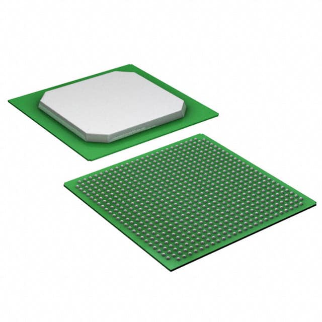
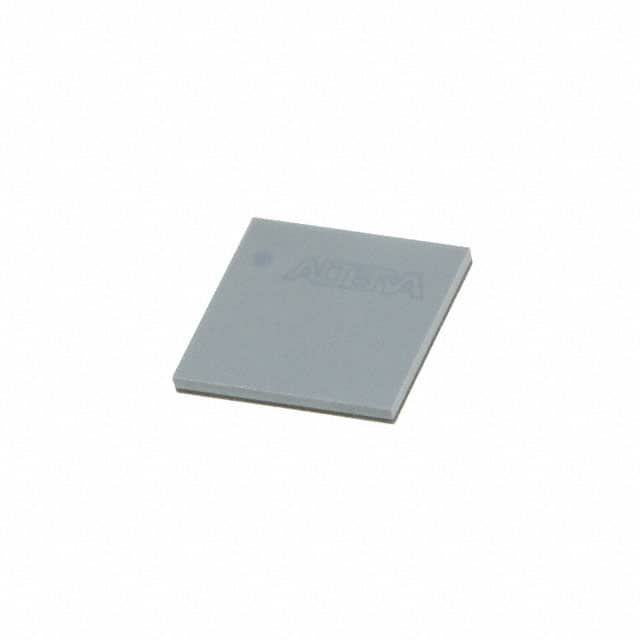
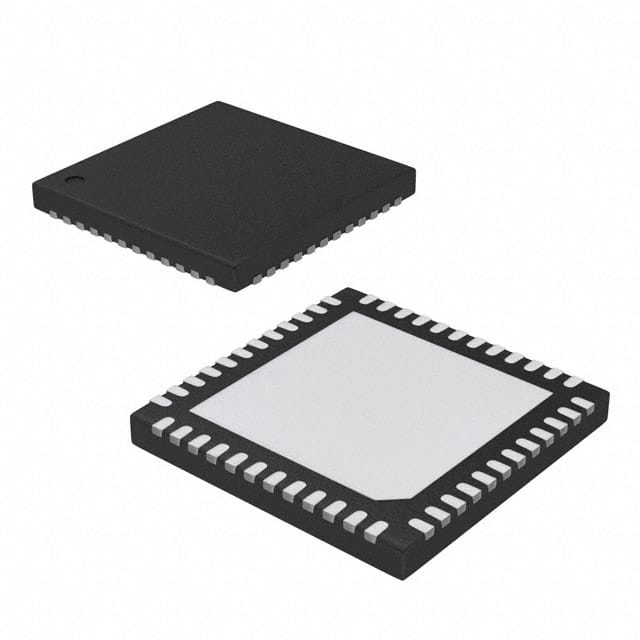
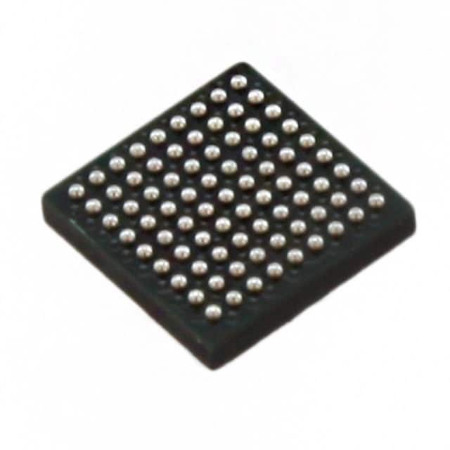
| Package | 672-pin FineLine BGA package, package code F27. |
| Operating Temperature | Industrial temperature grade, TJ = -40°C to +100°C. |
| Speed Grade | -7 FPGA fabric speed grade. |
| Packaging Compliance | Lead-free packaging option identified by N suffix. |
Pinout & Package
The 5CEFA9F27I7N pinout is based on a 672-pin FineLine BGA package. The device includes FPGA GPIO banks, configuration pins, clock inputs, PLL-related pins, memory-interface capable I/O, power and ground pins, JTAG pins, and dedicated pins required for Cyclone V configuration and operation.
For PCB implementation, the BGA escape pattern, bank voltage planning, power-rail decoupling, configuration scheme, clock routing, JTAG accessibility, and memory-interface signal integrity should be reviewed before layout. Since the device supports multiple I/O standards and high-speed external memory interfaces, each I/O bank should be assigned according to VCCIO compatibility, timing requirements, and board-level routing constraints.
| Pin / Function | PCB Design and Circuit Role |
|---|---|
| FPGA GPIO Banks | Provide programmable digital I/O for control, interface expansion, logic bridging, and custom protocol implementation. |
| VCC / Core Rails | Supply the FPGA core logic and require stable regulator design and local decoupling. |
| VCCIO Banks | Define I/O voltage levels for each bank and must match the selected interface standards. |
| Clock Inputs | Provide reference clocks for global clock networks, PLLs, memory interfaces, and synchronous FPGA logic. |
| PLL Resources | Support clock synthesis, zero-delay buffering, phase adjustment, and multi-clock FPGA designs. |
| External Memory Interface Pins | Support DDR3, DDR2, and LPDDR2 memory-controller connections when assigned in the design. |
| Configuration Pins | Support Active Serial, Passive Serial, Fast Passive Parallel, JTAG, and related configuration modes. |
| JTAG Pins | Used for programming, boundary scan, debugging, and production test access. |
| Ground Pins | Provide return paths for FPGA core, I/O banks, memory interfaces, and clock networks. |
| 672-Pin FineLine BGA | High-density FPGA package requiring controlled escape routing, via strategy, and thermal review. |
Key Features
- Cyclone V E FPGA optimized for enhanced logic, embedded memory, DSP, and external memory designs.
- 301K logic elements and 113,560 ALMs support large programmable logic implementations.
- 454,240 registers support deeply pipelined datapaths and register-rich FPGA designs.
- 12,200Kb M10K embedded memory supports buffers, FIFOs, frame memory, and RAM structures.
- 1,717Kb MLAB memory supports distributed LUTRAM, shift registers, and shallow memory arrays.
- 342 variable-precision DSP blocks provide configurable multiplier and accumulator resources.
- 684 equivalent 18 × 18 multipliers support filters, control algorithms, and numeric processing.
- Eight PLLs support complex clocking, frequency synthesis, deskew, and clock-domain management.
- Up to two hard memory controllers support DDR3, DDR2, and LPDDR2 interface designs.
- 336 GPIOs in the F672 package support broad board-level connectivity.
- Industrial temperature grade supports embedded and industrial operating environments.
- Lead-free FineLine BGA package supports high-density production PCB assembly.
Applications
| Industrial Control & Automation | Embedded Computing |
|---|---|
|
Use Scenario: PLC modules, machine controllers, motor-control platforms, field I/O systems, and industrial data-processing boards. FPGA Role: 5CEFA9F27I7N implements deterministic control logic, parallel interfaces, custom timing, data aggregation, and safety-related board logic. Use Value: Provides high logic density, industrial temperature support, and flexible I/O resources for long-life industrial platforms. |
Use Scenario: Embedded CPU companion logic, FPGA accelerator boards, custom bus bridges, and real-time processing modules. FPGA Role: Implements custom datapaths, register maps, memory interfaces, interrupt logic, and processor-connected acceleration blocks. Use Value: Reduces discrete logic and allows field-updatable hardware functionality. |
| Video, Imaging & DSP | Communication & Test Equipment |
|
Use Scenario: Video pipelines, image preprocessing, sensor fusion, filtering, and arithmetic-heavy real-time systems. FPGA Role: Uses variable-precision DSP blocks, embedded memory, and parallel logic to accelerate signal-processing functions. Use Value: Supports flexible low-latency processing without fixed-function ASIC constraints. |
Use Scenario: Protocol conversion, board-level test equipment, communication interfaces, timing generators, and data-capture platforms. FPGA Role: Provides programmable interface logic, memory buffering, clock management, and custom control-state machines. Use Value: Enables rapid hardware adaptation for multiple interface standards and product revisions. |
Equivalent & Alternatives
When evaluating 5CEFA9F27I7N equivalent devices, engineers should compare logic density, package footprint, GPIO count, memory resources, DSP resources, speed grade, industrial temperature support, hard memory controller count, configuration support, tool-chain compatibility, and existing firmware or bitstream qualification.
| Alternative Part | Technical Difference | Application Difference | Selection Advice |
|---|---|---|---|
| 5CEFA9F31I7N | Same Cyclone V E A9 density class with a larger 896-pin FBGA package and higher GPIO availability. | Used when the design requires more I/O pins or migration to a larger package. | Choose 5CEFA9F27I7N when the F672 package and 336 GPIO count match the existing PCB footprint. |
| 5CEFA7F27I7N | Lower A7 density class in a related Cyclone V E family option with fewer logic, memory, and DSP resources. | Used when the design fits a smaller FPGA resource budget but needs similar package-family support. | Choose 5CEFA9F27I7N when the design requires the larger A9 logic, DSP, and embedded memory resources. |
| 5CGXFC9D6F27I7N | Cyclone V GX device with 3Gbps transceivers and PCIe hard IP options, but different family variant and feature positioning. | Used when serial transceivers or PCIe hard IP are required in addition to FPGA fabric. | Choose 5CEFA9F27I7N when high-speed serial transceivers are not required and Cyclone V E logic/memory resources are preferred. |
| XC7A200T | Xilinx Artix-7 FPGA alternative with different architecture, tool chain, package options, and resource mapping. | Used in similar FPGA logic, DSP, and embedded processing-support designs after full redesign and requalification. | Choose 5CEFA9F27I7N when Intel Quartus project compatibility, Cyclone V pinout, and existing board qualification must be maintained. |
Compared with 5CEFA9F31I7N, 5CEFA9F27I7N is optimized for designs that need the A9 density class in the smaller F672 package instead of the larger F896 package. 5CEFA9F27I7N vs 5CEFA7F27I7N selection depends on logic utilization, embedded memory demand, DSP block usage, I/O planning, timing closure, package compatibility, and sourcing continuity requirements.
Quality
5CEFA9F27I7N should be sourced as original Intel FPGA components through traceable and controlled supply channels. Quality verification procedures may include package inspection, top-mark validation, BGA ball inspection, solderability review, JTAG identification, configuration testing, boundary-scan validation, memory-interface test, and incoming inspection according to FPGA production requirements.
Because the device is a high-density BGA FPGA, long-term reliability depends on validated PCB footprint design, power-rail sequencing, decoupling strategy, I/O bank voltage planning, configuration-memory compatibility, thermal design, clock-tree planning, timing closure, and verified Quartus compilation constraints. Traceable sourcing supports manufacturing quality and reduces counterfeit supply-chain risk for programmable logic production programs.
Availability
5CEFA9F27I7N available at Aetrix Electronics and suitable for industrial control, embedded computing, communication equipment, video processing, test platforms, memory-interface systems, and programmable logic applications requiring stable component supply and repeatable production support.
Supply support may include scheduled delivery planning, volume procurement support, BOM continuity assistance, traceable sourcing management, and long-term availability support for OEM manufacturers, FPGA board developers, industrial-control designers, communication-equipment builders, and electronics production programs.
For production deployment, confirming FPGA density, package code, speed grade, temperature grade, GPIO usage, DSP utilization, memory-controller requirements, configuration method, and sourcing continuity helps reduce procurement risk and improve manufacturing stability.
Manufacturer
Intel is a semiconductor manufacturer providing processors, FPGAs, programmable logic devices, connectivity products, embedded solutions, data-center platforms, memory-related technologies, and development software for industrial, communication, computing, automotive, consumer, and infrastructure applications.
The Intel Cyclone V FPGA portfolio focuses on low-power programmable logic, cost-efficient FPGA integration, embedded memory, variable-precision DSP, hard memory controllers, configurable I/O, and flexible configuration features for industrial systems, embedded computing, communication equipment, video processing, and board-level control designs.
FAQ
What is 5CEFA9F27I7N used for?
5CEFA9F27I7N is used for industrial control, embedded computing, DSP acceleration, video processing, interface bridging, memory-interface control, communication equipment, and high-density programmable logic applications.
Where can I find the 5CEFA9F27I7N datasheet download?
The 5CEFA9F27I7N datasheet and Cyclone V device documentation are available from Intel and include ordering-code details, family features, resource tables, package plans, configuration options, memory-interface support, DSP architecture, and I/O information.
What does the 5CEFA9F27I7N ordering code mean?
5CEFA9F27I7N identifies a Cyclone V E FPGA with F embedded hard-IP option, A9 density class, 672-pin FineLine BGA package, industrial temperature grade, -7 fabric speed grade, and lead-free packaging.
Does 5CEFA9F27I7N include high-speed transceivers?
No. 5CEFA9F27I7N belongs to the Cyclone V E family, which is optimized for enhanced logic, memory, DSP, GPIO, and memory-controller applications. Designs requiring high-speed serial transceivers should evaluate Cyclone V GX or GT variants instead.
What are common 5CEFA9F27I7N equivalent solutions?
Common alternatives include 5CEFA9F31I7N, 5CEFA7F27I7N, selected Cyclone V GX devices, and comparable FPGA families depending on resource usage, package footprint, I/O count, transceiver needs, speed grade, temperature range, and tool-chain compatibility.
Reference checked against the uploaded Intel Cyclone V Device Overview, including the Cyclone V E ordering-code diagram, A9 resource table, package plan, feature summary, DSP, memory, and configuration sections. :contentReference[oaicite:0]{index=0}
5CEFA9F27I7N Specifications
- Product attributes
- Attribute value
- Manufacturer:
- Intel
- Series:
- Cyclone® V E
- Package/Case:
- 672-BGA
- Packaging:
- Tray
- Product Status:
- Active
- Programmable:
- Not Verified
- Number of LABs/CLBs:
- 113560
- Number of Logic Elements/Cells:
- 301000
- Total RAM Bits:
- 14251008
- Number of I/O:
- 336
- Number of Gates:
- -
- Voltage - Supply:
- 1.07V ~ 1.13V
- Mounting Type:
- Surface Mount
- Operating Temperature:
- -40°C ~ 100°C (TJ)
- Grade:
- -
- Qualification:
- -
- Supplier Device Package:
- 672-FBGA (27x27)
5CEFA9F27I7N FAQ
1.How can I place an order for 5CEFA9F27I7N through Aetrix?
Please submit a Request for Quotation (RFQ) for 5CEFA9F27I7N on Aetrix. Our sales agent will provide a competitive quotation and guide you through the order confirmation once you accept the terms.
2.Are the price and stock information for 5CEFA9F27I7N reliable?
The price and inventory of 5CEFA9F27I7N are updated periodically and may fluctuate due to market conditions. Stock and pricing data are typically refreshed every 24 hours. Quotation validity for 5CEFA9F27I7N is usually 5 days.
3.What payment methods are accepted for 5CEFA9F27I7N?
We accept Wire Transfer, PayPal, Credit Card, Western Union, MoneyGram, and Escrow for 5CEFA9F27I7N transactions.
Note: Certain payment methods may incur a processing fee.
4.How is shipping managed for 5CEFA9F27I7N?
5CEFA9F27I7N orders can be shipped via leading logistics carriers, including DHL, UPS, FedEx, TNT, or Registered Mail.
Once your 5CEFA9F27I7N order is processed, you will receive an email with the shipment details and tracking number.
Note: Tracking information may take up to 24 hours to appear. Express delivery typically takes 3–5 business days.
5.How can I obtain technical support or documentation for 5CEFA9F27I7N?
For technical support, including 5CEFA9F27I7N datasheets, pinout diagrams, or application guidance, please contact our engineering support team. They can provide detailed documentation and assistance for your 5CEFA9F27I7N requirements.
6.How does Aetrix verify that 5CEFA9F27I7N is sourced from the original manufacturer or authorized distributors?
All 5CEFA9F27I7N products on Aetrix are procured from qualified distributors and authorized channels. Our dedicated quality assurance team conducts strict verification, including traceability checks and, if necessary, third-party testing. This ensures that 5CEFA9F27I7N meets industry standards.
7.What is the process for return or replacement of 5CEFA9F27I7N?
All 5CEFA9F27I7N units undergo pre-shipment inspection (PSI). If there is an issue with 5CEFA9F27I7N, returns or replacements are accepted under the following conditions:
1.Quantity discrepancies, incorrect items, or visible external defects (such as breakage or corrosion), acknowledged by Aetrix.
2.The issue is reported within 90 days of delivery.
3.The 5CEFA9F27I7N part is unused and in its original packaging.
Return procedure for 5CEFA9F27I7N:
1.Submit a request within 90 days.
2.Obtain a Return Material Authorization (RMA) from Aetrix.
5CEFA9F27I7N Tags
-
ICE40LP384-SG32
Lattice Semiconductor Corporation
-
ICE40UL640-CM36AI
Lattice Semiconductor Corporation
-
ICE40UL1K-CM36AI
Lattice Semiconductor Corporation
-
LCMXO2-256HC-4SG32C
Lattice Semiconductor Corporation
-
10M02DCV36C8G
Intel
-
LCMXO2-256HC-4SG32I
Lattice Semiconductor Corporation
-
ICE5LP1K-SG48ITR
Lattice Semiconductor Corporation
-
ICE40LP1K-CM36
Lattice Semiconductor Corporation
-
LCMXO2-256ZE-1SG32I
Lattice Semiconductor Corporation
-
LCMXO2-256HC-4SG48I
Lattice Semiconductor Corporation
-
ICE40LP1K-CM81
Lattice Semiconductor Corporation

-
T20W80I4
Efinix, Inc.
Tech Hub
Amplifier guide covering voltage, current and power amplification, gain, feedback, amplifier classes, audio and RF applications, op-amp circuits, transimpedance amplifiers, datasheet selection and trou…

Machine vision system guide covering components, inspection workflow, camera and lens selection, FOV, pixel resolution, motion blur, strobe lighting, bandwidth, 2D/3D vision, integration, troubleshooti…
Electronic devices and circuits guide covering passive components, semiconductors, analog and digital circuits, circuit theory, practical calculations, troubleshooting, datasheet selection, and learnin…
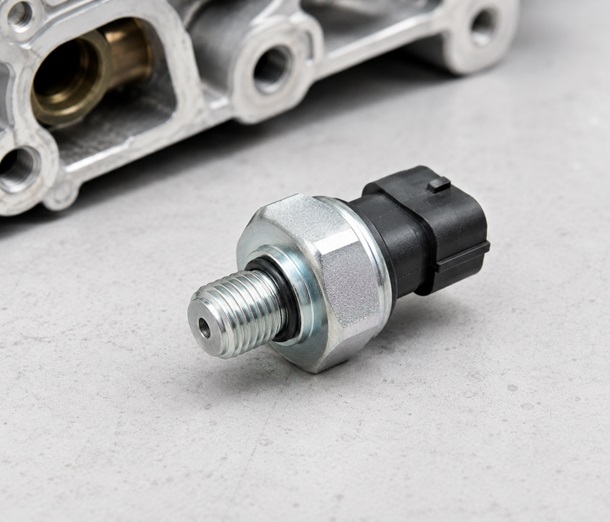
Oil pressure sensor diagnosis covering symptoms, location, testing, replacement, socket access, common failure cases, and the electronic signal path between the pressure sensor, wiring, ECU and gauge s…
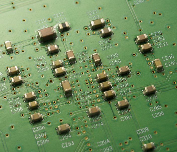
MLCC ESR, impedance and self-resonant frequency in decoupling networks. Covers PDN behavior, frequency response, measurement methods, failure cases and practical capacitor selection for power integrity…
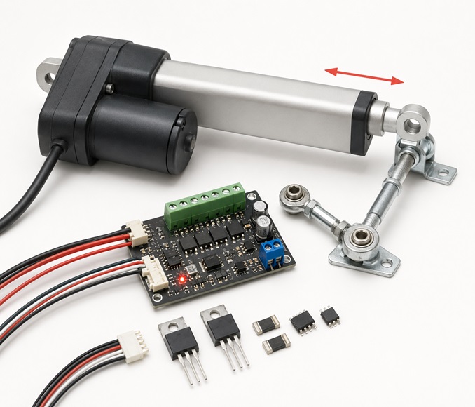
An actuator converts a control signal and energy source into mechanical motion. This guide explains actuator types, working principles, electric and linear actuators, automotive use cases, troubleshoot…
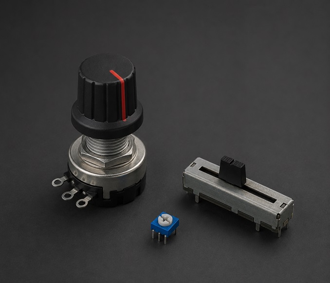
A potentiometer is a three-terminal adjustable resistor used for voltage division, analog control, calibration and signal adjustment. This guide explains wiring, symbols, types, 10k values, digital pot…
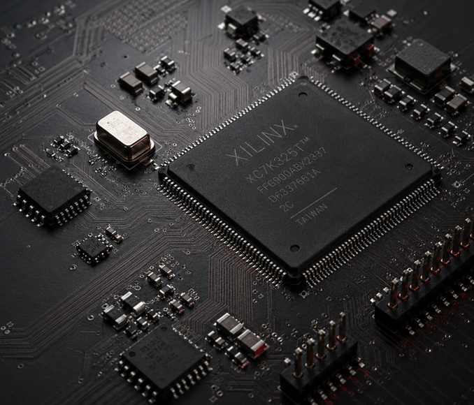
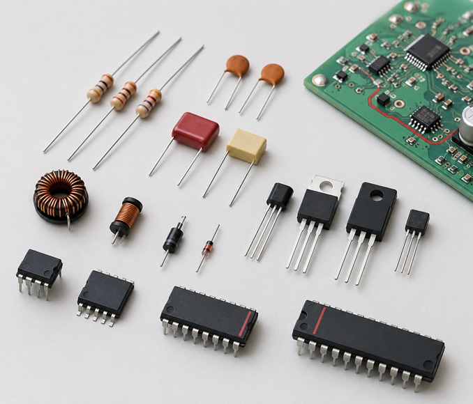
An FPGA is reconfigurable digital hardware used for custom logic, parallel processing, low-latency I/O and interface control. This guide explains FPGA meaning, architecture, boards, programming flow, a…
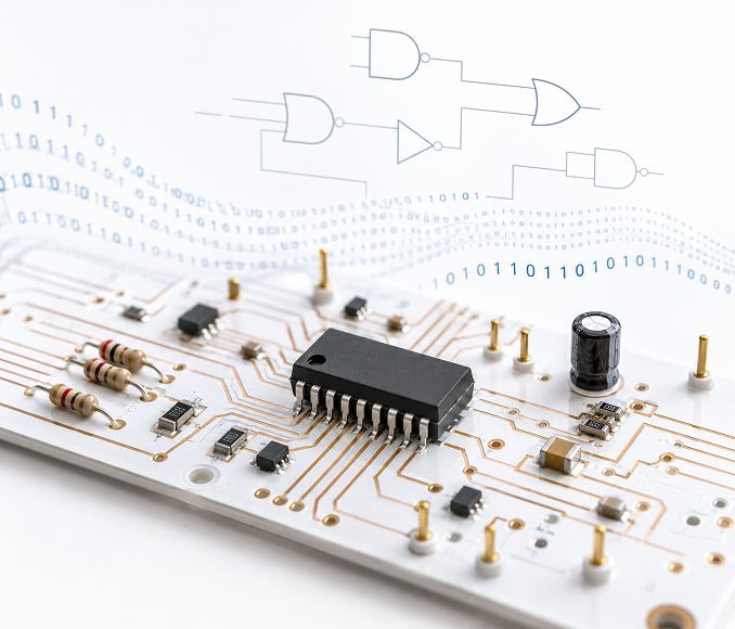
A logic gate is a basic digital circuit that uses Boolean logic to convert binary inputs into one output. This guide explains AND, OR, NOT, NAND, NOR, XOR, truth tables, universal gates, logic ICs and …
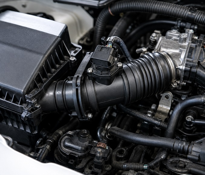
A mass air flow sensor, often called a MAF sensor, measures the amount of air entering an engine.