Send an Inquiry

To receive a quote for your project, please fill in the following information, and we’ll get back to you promptly.

Name*
Company*
Email Address*
Phone/WhatsApp
Part Number*
Quantity*
Message
Submit Inventory List

Please fill in the following information, and we’ll get back to you promptly.

Name*
Company*
Email Address*
Phone/WhatsApp
Upload My List
Message

Semtech Corporation ACS8947T

Part No.:
ACS8947T
Manufacturer:
Semtech Corporation
Category:
Application Specific Clock/Timing
Package:
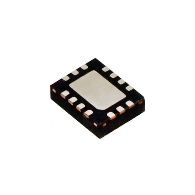
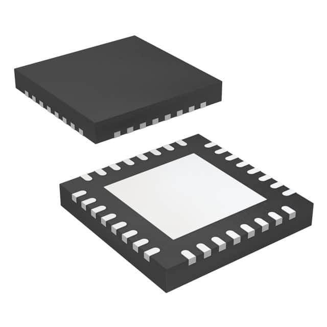
48-VFQFN Exposed Pad
Datasheet:
AetrixACS8947T.pdf
Description:
IC JITTER ATT MULT PLL 48-QFN
Quantity:
Payment:
Payment
Shipping:
Shipping

Inventory:2,138

Please send an inquiry. Send us your inquiry, and we will respond immediately.

Part Number
Quantity*
Price
Name*
Company
Email*
Comments

Product details

Overview

The ACS8947T from Semtech is a jitter-attenuating, integer-N phase-locked loop IC with integrated VCO, two LVPECL differential reference inputs (580 kHz–180 MHz), four independently powered LVPECL/CML differential outputs (up to 625 MHz), hardwired configuration, and automatic input switching-used for clock cleaning in SONET/SDH OC-12, Ethernet, and wireless baseband systems.

For engineers reviewing the ACS8947T datasheet, pinout, applications, or equivalent options, this page delivers verified PLL architecture details, confirmed QFN48 package mapping, validated output jitter (2.8 ps RMS in OC-12), hardwired configuration logic, and real-world resynchronization behavior with SYNC_IN/SYNC_OUT path.

Technical Context

The ACS8947T implements an integer-N PLL with integrated 2.35–2.9 GHz VCO, external differential loop filter (VCP/VCN), and programmable closed-loop bandwidth (≥2 kHz). It supports frequency translation via configurable input (DIVIP), feedback (DIVFB), and odd (DIVODD) dividers, enabling spot-frequency synthesis from 1.23 MHz to 625 MHz.

Input selection uses activity monitoring on CLK1P/N and CLK2P/N with non-revertive automatic switching; the SYNC path resynchronizes an external 8 kHz signal to OUT1's rising edge. Lock detection is analog (LOCKB pulse-width modulated current), and all configuration is static via 12 CFG_IN pins tied to power/ground/alarm outputs.

Key Specifications

Parameter Value and Actual Design Meaning
VCO Frequency Range 2.35 GHz to 2.9 GHz - enables generation of high-frequency clean clocks up to 625 MHz via integer division.
Input Frequency Range 580 kHz to 180 MHz - supports legacy telecom (E1/DS1), Ethernet (25/62.5 MHz), and 3G (3.84 MHz) references without level-shifting.
Output Frequency Range 1.23 MHz to 625 MHz - covers SONET OC-12 (622.08 MHz), PCI (133 MHz), and memory interface (167 MHz) requirements.
Output Jitter (RMS) 2.8 ps in SONET/SDH OC-12 system - meets Telcordia GR-1244-CORE jitter compliance for line-card clock recovery.
Closed-Loop Bandwidth Configurable from 2 kHz upward - allows trade-off between jitter attenuation and tracking of wander in telecom applications.
Tracking Range ±200 ppm - ensures stable lock under temperature- and aging-induced reference drift in carrier-grade systems.
Supply Voltage +3.3 V (±5% for most rails; −10% tolerance on VDDOSC) - requires separate low-noise supplies for VCO, PFD, and outputs to minimize supply-induced phase noise.

Pinout & Package

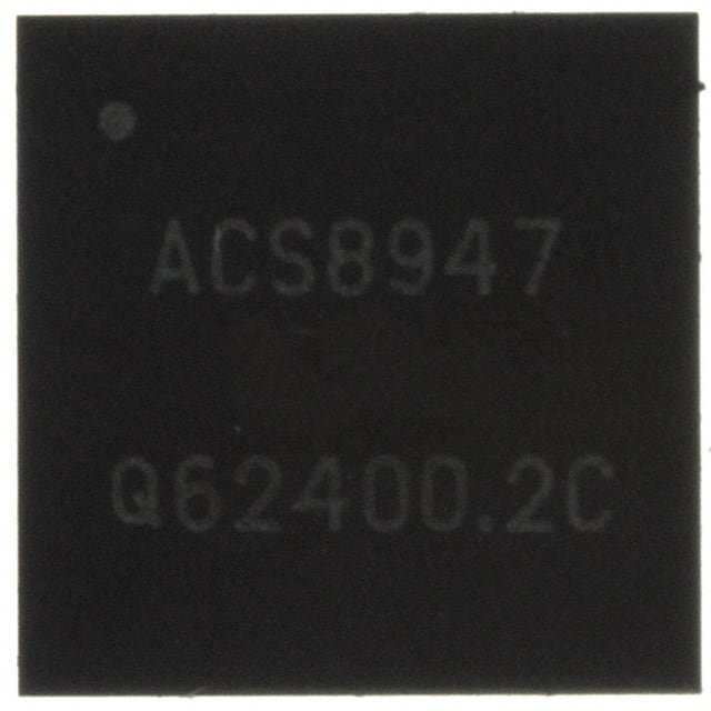
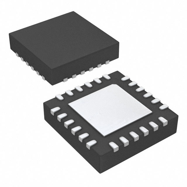
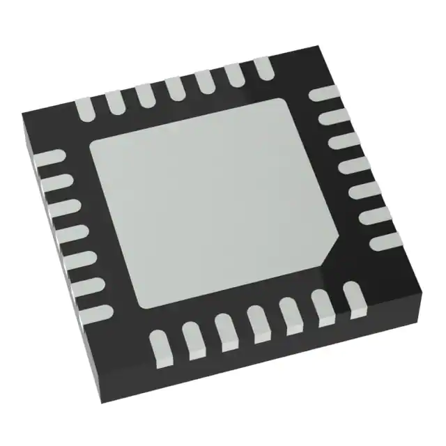
The ACS8947T is housed in a 7 mm × 7 mm × 0.9 mm leadless QFN48 package with exposed thermal pad (VSS0, Pin 49). Power domains are isolated: VDDO1–VDDO4 for individual outputs, VDDADIV for divider stages, VDDP1/VDDP2 for inputs/config, VDDARF for PFD, and VDDOSC/VSSOSC for VCO.

Pin/Terminal Circuit Role Design Meaning
OUT1P/OUT1N (Pins 3/2) Differential clock output pair LVPECL or CML output; frequency set by hardwired dividers; enabled only when VDDO1 = 3.3 V.
CLK1P/CLK1N (Pins 28/27) Differential reference input pair LVPECL-compatible primary reference; accepts 580 kHz–180 MHz; monitored by ALARM1_CO0 for failure detection.
CLK2P/CLK2N (Pins 31/30) Differential reference input pair LVPECL-compatible secondary reference; same frequency range; monitored by ALARM2_CO1.
SYNCP/SYNCN (Pins 41/42) Differential resync input pair Accepts up to 40 MHz sync signal (typically 8 kHz); resynchronized to rising edge of OUT1 for deterministic timing alignment.
SYNC_OUT (Pin 44) Resynchronized sync output LVCMOS-level output synchronized to OUT1 rising edge; requires OUT1 ≥ 2× SYNC frequency and ≤ 80 MHz.
LOCKB (Pin 17) Analog lock detect Pulse-width modulated current output (≈10 μA/pulse); RC-filtered voltage indicates lock status (low = locked).
CFG_IN[11:0] (Pins 18–25, 45–48) Hardwire configuration inputs 12 LVTTL/LVCMOSD pins; tied to VDD/GND/ALARM outputs per GUI-generated wiring map to define dividers and modes.
RESETB (Pin 40) Active-low reset Schmitt-trigger input with internal pull-up; initiates fast-lock scan and reloads configuration on falling edge.

Key Features

Feature Design Value
Hardwired configuration matrix Eliminates need for external microcontroller or I²C interface-configuration is set at power-up via resistor ties to CFG_IN pins.
Four independent output supplies (VDDO1–VDDO4) Enables selective output enable/disable per channel to reduce dynamic power and isolate noise domains in multi-clock systems.
Non-revertive automatic input switching Prevents oscillation during transient clock faults-once switched to CLK2 due to CLK1 failure, it remains on CLK2 even after CLK1 recovers.
Dual alarm hierarchy (ALARM1_CO0/ALARM2_CO1 vs. ALARMC_CO3) Coarse input failure detection (6 missing cycles) plus fine PFD-level alarm (3 missing edges) enables robust failover in bursty or marginally stable references.
External feedback mode Supports precise phase alignment when driving long traces or buffers by feeding back from output path instead of internal divider.

Applications

SONET/SDH Line Card Clock Cleaning Ethernet PHY Timing Recovery

Use Scenario: Recovering low-jitter 622.08 MHz clock from degraded OC-12 data stream in optical transport equipment.

IC Role / Device Role / Timing Role: Jitter-attenuating PLL that cleans incoming reference and regenerates compliant output using internal VCO and external loop filter.

Use Value: Achieves 2.8 ps RMS jitter-meeting GR-253-CORE OC-12 mask-enabling reliable 10 Gbps serial link operation without external VCXO.

Use Scenario: Generating synchronized 125 MHz and 250 MHz clocks for 10GBASE-R and SFP+ transceivers in switch fabric line cards.

IC Role / Device Role / Timing Role: Frequency-multiplying PLL with dual reference inputs, allowing seamless failover between primary and backup system clocks.

Use Value: Four independent outputs support multiple PHY layers simultaneously; hardwired config eliminates boot-time firmware dependency in carrier switches.

3G/4G Baseband Synchronization PCI Express Gen1 Clock Generation

Use Scenario: Providing phase-aligned 61.44 MHz and 30.72 MHz clocks for WCDMA femtocell baseband processors and ADC/DAC interfaces.

IC Role / Device Role / Timing Role: Integer-N PLL with resynchronization path, aligning baseband timing to external 8 kHz frame sync signal.

Use Value: SYNC_OUT output aligned to OUT1 rising edge enables deterministic sample timing across RF and digital domains-critical for EVM compliance.

Use Scenario: Delivering 100 MHz PCIe reference clock with sub-1 ps added jitter to multiple slots in industrial server backplanes.

IC Role / Device Role / Timing Role: Low-jitter clock generator with independent output supplies, allowing per-slot enable/disable and isolation from shared power rail noise.

Use Value: Meets PCIe Gen1 jitter spec (≤1.5 ps RMS) while supporting hot-plug slot management via VDDOx control.

Equivalent & Alternatives

The following parts are listed as comparable options for similar jitter-attenuating PLL applications.

Alternative Part Technical Difference Application Difference Selection Advice
ICS8430I Lower max output frequency (350 MHz), no SYNC resync path, requires I²C programming; single 3.3 V supply (no isolated VDD domains). Targeted at cost-sensitive enterprise networking-not carrier-grade SONET or 3G sync-critical systems. Choose ICS8430I only if I²C control is acceptable and OC-12/3G timing compliance is not required.
Si5338A Multi-synth architecture (not integer-N), integrated crystal option, programmable via I²C/SPI; higher integration but no hardwired config. Designed for flexible multi-rate clock generation in FPGA-based platforms-not fixed-frequency telecom line cards. Choose Si5338A when field reprogrammability and crystal integration outweigh need for zero-software boot and deterministic lock behavior.

Compared with ICS8430I and Si5338A, the ACS8947T uniquely delivers hardwired configuration, 625 MHz output capability, dedicated SYNC resynchronization, and telecom-grade jitter performance without software dependency-making it optimal for carrier infrastructure where deterministic timing and firmware-free operation are mandatory.

Availability

The ACS8947T is available at Aetrix Electronics and suitable for SONET/SDH line cards, Ethernet switch fabric timing, 3G/4G baseband synchronization, PCI Express clock distribution, and wireless infrastructure requiring stable component supply across extended product lifecycles.

Supply support for ACS8947T includes scheduled delivery planning, volume procurement assistance, BOM continuity management, traceable sourcing, and lifecycle availability coordination for OEM customers, industrial embedded developers, connected-device designers, and electronics production programs.

Manufacturer

Semtech Corporation is a U.S.-based fabless semiconductor company specializing in high-performance analog and mixed-signal ICs for advanced communications, sensing, and power management.

The ACS8947T belongs to Semtech's Advanced Communications & Sensing product line, designed specifically for jitter-critical telecom and datacom timing applications requiring deterministic lock, automatic failover, and hardware-only configuration.

FAQ

What is the maximum output frequency supported by the ACS8947T?

The ACS8947T supports a maximum output frequency of 625 MHz on each of its four differential outputs. This is achieved using the internal 2.35–2.9 GHz VCO with integer division, and is validated in Ethernet (625 MHz) and SONET OC-12 (622.08 MHz) configurations per the official datasheet. Output frequency is set at power-up via hardwired CFG_IN pin states and cannot be dynamically changed.

Does the ACS8947T require a microprocessor for configuration?

No, the ACS8947T does not require a microprocessor. All configuration-including input selection, divider ratios, output format (LVPECL/CML), and SYNC enable-is performed at power-up via hardwired connections of the 12 CFG_IN pins to VDD, GND, or alarm outputs (ALARM1_CO0, etc.), as defined by Semtech's evaluation GUI tool. This enables firmware-free, deterministic startup.

How does the automatic input switching work on the ACS8947T?

The ACS8947T uses ALARM1_CO0 and ALARM2_CO1 to monitor activity on CLK1P/N and CLK2P/N, respectively, and ALARMC_CO3 to monitor the currently selected input at the PFD. In automatic mode (AUTO_SEL=1, SEL_CLK2=1), it performs non-revertive switching: if CLK1 fails and the device switches to CLK2, it remains on CLK2 even after CLK1 recovers-preventing oscillation during marginal conditions.

What is the purpose of the SYNC_IN and SYNC_OUT pins on the ACS8947T?

The SYNC_IN pins (SYNCP/SYNCN, Pins 41/42) accept an external timing reference (e.g., 8 kHz frame sync) and resynchronize it to the rising edge of the OUT1 clock. The resulting aligned signal appears on SYNC_OUT (Pin 44) as an LVCMOS output. This enables deterministic phase alignment between baseband processing and RF sections in 3G/4G systems, provided OUT1 frequency is ≥2× and ≤80 MHz.

What package type and dimensions does the ACS8947T use?

The ACS8947T uses a 48-pin QFN package with 7 mm × 7 mm body size and 0.9 mm height, featuring an exposed thermal pad (Pin 49, VSS0). This small-form-factor package supports high-density PCB layouts in telecom line cards and wireless baseband modules while enabling efficient thermal dissipation through the central ground pad.

ACS8947T Specifications

Product attributes
Attribute value
Manufacturer:
Semtech Corporation
Series:
-
Package/Case:
48-VFQFN Exposed Pad
Packaging:
Tray
Product Status:
Obsolete
Programmable:
Not Verified
PLL:
Yes
Main Purpose:
3G, Ethernet, PCI, SONET/SDH, Wireless systems
Input:
LVPECL
Output:
CML, LVPECL
Number of Circuits:
1
Ratio - Input:Output:
2:4
Differential - Input:Output:
Yes/Yes
Frequency - Max:
625MHz
Voltage - Supply:
3.135V ~ 3.465V
Operating Temperature:
-40°C ~ 85°C
Mounting Type:
Surface Mount
Grade:
-
Qualification:
-
Supplier Device Package:
48-QFN (7x7)

ACS8947T FAQ

1.How can I place an order for ACS8947T through Aetrix?

Please submit a Request for Quotation (RFQ) for ACS8947T on Aetrix. Our sales agent will provide a competitive quotation and guide you through the order confirmation once you accept the terms.

2.Are the price and stock information for ACS8947T reliable?

The price and inventory of ACS8947T are updated periodically and may fluctuate due to market conditions. Stock and pricing data are typically refreshed every 24 hours. Quotation validity for ACS8947T is usually 5 days.

3.What payment methods are accepted for ACS8947T?

We accept Wire Transfer, PayPal, Credit Card, Western Union, MoneyGram, and Escrow for ACS8947T transactions.

Note: Certain payment methods may incur a processing fee.

4.How is shipping managed for ACS8947T?

ACS8947T orders can be shipped via leading logistics carriers, including DHL, UPS, FedEx, TNT, or Registered Mail.

Once your ACS8947T order is processed, you will receive an email with the shipment details and tracking number.

Note: Tracking information may take up to 24 hours to appear. Express delivery typically takes 3–5 business days.

5.How can I obtain technical support or documentation for ACS8947T?

For technical support, including ACS8947T datasheets, pinout diagrams, or application guidance, please contact our engineering support team. They can provide detailed documentation and assistance for your ACS8947T requirements.

6.How does Aetrix verify that ACS8947T is sourced from the original manufacturer or authorized distributors?

All ACS8947T products on Aetrix are procured from qualified distributors and authorized channels. Our dedicated quality assurance team conducts strict verification, including traceability checks and, if necessary, third-party testing. This ensures that ACS8947T meets industry standards.

7.What is the process for return or replacement of ACS8947T?

All ACS8947T units undergo pre-shipment inspection (PSI). If there is an issue with ACS8947T, returns or replacements are accepted under the following conditions:

1.Quantity discrepancies, incorrect items, or visible external defects (such as breakage or corrosion), acknowledged by Aetrix.

2.The issue is reported within 90 days of delivery.

3.The ACS8947T part is unused and in its original packaging.

Return procedure for ACS8947T:

1.Submit a request within 90 days.

2.Obtain a Return Material Authorization (RMA) from Aetrix.

ACS8947T Tags
  • ACS8947T
  • ACS8947T PDF
  • ACS8947T Datasheet
  • ACS8947T Specifications
  • ACS8947T Images
  • Semtech Corporation
  • Semtech Corporation ACS8947T
  • Buy ACS8947T
  • ACS8947T Price
  • ACS8947T Distributor
  • ACS8947T Supplier
  • ACS8947T Wholesale
Related Products
LMK00334RTVRQ1
LMK00334RTVRQ1

Texas Instruments

DSC557-0344FI0T
DSC557-0344FI0T

Microchip Technology

9FGV0241AKILFT
9FGV0241AKILFT

Renesas

9DBL0452CKILFT
9DBL0452CKILFT

Renesas

DSC557-0344FL1T
DSC557-0344FL1T

Microchip Technology

RC19008AGND#KB0
RC19008AGND#KB0

Renesas

RC19008AGND#BB0
RC19008AGND#BB0

Renesas

9DB403DGILFT
9DB403DGILFT

Renesas

9DB233AGILFT
9DB233AGILFT

Renesas

9DB803DGILFT
9DB803DGILFT

Renesas

9FGL0851DKILFT
9FGL0851DKILFT

Renesas

AB-557-03-HCHC-F-L-C-T

Abracon LLC

Tech Hub

Search

Search

PRODUCT

PRODUCT

PHONE

PHONE

USER

USER