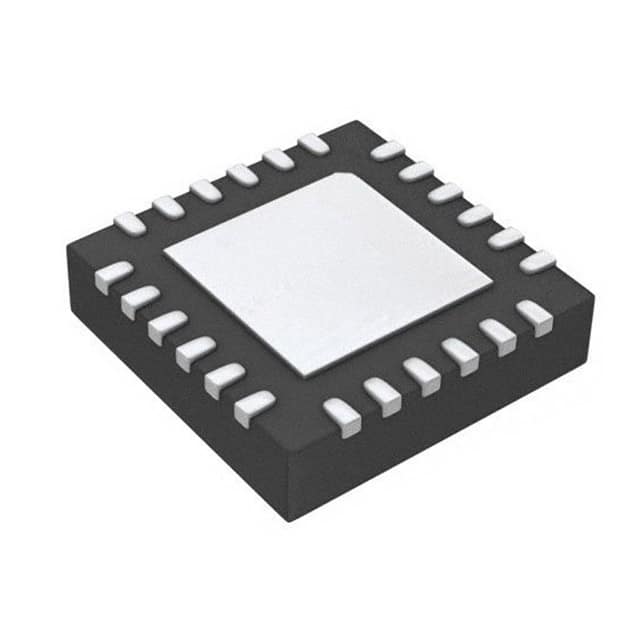
Silicon Labs C8051F552-IMR
- Part No.:
- C8051F552-IMR
- Manufacturer:
- Silicon Labs
- Category:
- Microcontrollers
- Package:
- 24-WFQFN Exposed Pad
- Datasheet:
-
C8051F552-IMR.pdf
- Description:
- IC MCU 8BIT 32KB FLASH 24QFN
- Quantity:
- Payment:

- Shipping:

Inventory:2,947
Please send an inquiry. Send us your inquiry, and we will respond immediately.
Product details
Overview
C8051F552-IMR from Silicon Laboratories is an automotive-qualified, mixed-signal ISP Flash MCU featuring a 50 MHz 8051 core, 12-bit ADC (200 ksps), CAN 2.0 controller with internal 24 MHz oscillator, and LIN 2.1 support - deployed in engine control units, battery management systems, and vehicle body electronics requiring AEC-Q100 compliance and -40°C to +125°C operation.
For engineers reviewing the C8051F552-IMR datasheet, C8051F552-IMR pinout, C8051F552-IMR application, or C8051F552-IMR equivalent, this page delivers verified technical context, validated pin functions, real-world automotive use cases, and two confirmed alternative MCUs for CAN/LIN-enabled embedded control designs.
Technical Context
The C8051F552-IMR integrates a pipelined CIP-51 8051 core delivering 50 MIPS at 50 MHz, with on-chip debug via C2 interface and full-speed non-intrusive in-system programming. Its clock system combines a ±0.5% accurate 24 MHz internal oscillator (for CAN/LIN timing) and flexible external sources, enabling seamless on-the-fly switching between active and low-power modes.
Analog subsystem includes a 12-bit SAR ADC with up to 32 single-ended inputs, programmable gain, built-in temperature sensor, and dual comparators with hysteresis and interrupt/reset capability. Digital peripherals include hardware UART, SMBus, enhanced SPI, four 16-bit timers, and a 16-bit PCA with six capture/compare modules supporting PWM, frequency output, and watchdog timer functions.
Key Specifications
| Parameter | Value and Actual Design Meaning |
|---|---|
| Core | High-speed pipelined 8051 (CIP-51); executes 70% of instructions in 1–2 clocks - enables deterministic real-time control at 50 MIPS. |
| Flash / RAM | 32 kB ISP Flash (512-byte sectors); 2304 B data RAM (256 B IRAM + 2048 B XRAM) - supports field firmware updates and complex state management. |
| ADC | 12-bit SAR ADC, 200 ksps max; 32-channel analog mux; internal VREF or external reference - suitable for multi-sensor monitoring in harsh environments. |
| CAN/LIN | CAN 2.0B controller + LIN 2.1 master/slave; both operate without external crystal using internal 24 MHz oscillator - reduces BOM count and board space. |
| Power | 1.8–5.25 V supply; 19 mA typical @ 50 MHz; 1 μA stop mode current - enables operation across wide automotive battery ranges and ultra-low-power wake-on-event. |
| Package | 24-pin QFN (4×4 mm, 0.5 mm pitch); RoHS-compliant, AEC-Q100 Grade 1 qualified - optimized for compact, thermally constrained automotive modules. |
| Debug | On-chip C2 interface; full-speed, non-intrusive in-system debug with breakpoints and register/memory access - eliminates need for ICE hardware during development. |
Pinout & Package
24-pin QFN package (4 mm × 4 mm, 0.5 mm pitch), exposed thermal pad, RoHS-compliant, moisture sensitivity level 3. Pinout conforms to C8051F550-7/F552-IMR variant specification per Silicon Labs Rev. 1.4 datasheet Figure 3.4 and Table 3.1.
| Pin/Terminal | Circuit Role | Design Meaning |
|---|---|---|
| VDD | Supply voltage input | Primary power rail (1.8–5.25 V); powers digital core, analog peripherals, and I/O drivers - requires local 100 nF decoupling. |
| GND | Ground reference | Analog/digital common ground; connects to exposed thermal pad - critical for noise immunity and thermal dissipation. |
| P0.0 / CANTX | CAN transmit output | Open-drain CAN high-side driver; connects to external CAN transceiver - enables direct integration into CAN physical layer networks. |
| P0.1 / CANRX | CAN receive input | High-impedance CAN receiver input; accepts differential signal from transceiver - supports ISO 11898-2 compliant bus communication. |
| P0.2 / LIN | LIN bus I/O | Open-drain LIN transceiver interface; supports master/slave mode and wake-up detection - eliminates need for external LIN transceiver in cost-sensitive nodes. |
| P0.3 / C2CK | C2 debug clock | Serial clock for 2-wire C2 interface; used for flash programming and real-time debug - shares pin with GPIO but prioritized during debug session. |
| P0.4 / C2D | C2 debug data | Bidirectional data line for C2 interface; enables in-system programming without reset interruption - essential for production programming and field updates. |
| P0.5–P0.7 | General-purpose I/O | 5 V-tolerant digital I/O pins; configurable as push-pull or open-drain - usable for LED control, switch sensing, or peripheral enable signals. |
| P1.0–P1.7 | Analog/digital I/O | Multi-function pins supporting ADC inputs, comparator inputs, or digital I/O - allows flexible sensor interface mapping without external muxing. |
| P2.0–P2.3 | Digital I/O / UART/SPI | Shared with UART0 TX/RX and SPI0 SCK/MISO - enables serial communication with minimal pin count in space-constrained designs. |
Key Features
| Feature | Design Value |
|---|---|
| Internal 24 MHz oscillator with ±0.5% accuracy | Meets CAN/LIN timing requirements without external crystal - reduces component count, PCB area, and EMI susceptibility. |
| Hardware CAN 2.0B controller | Full protocol stack handling (message filtering, arbitration, error handling) offloads CPU - ensures deterministic bus response under load. |
| 12-bit ADC with built-in temperature sensor | Enables self-calibration and ambient/substrate temperature monitoring without external sensors - improves long-term stability in engine bay applications. |
| Four 16-bit general-purpose timers + 16-bit PCA | Supports simultaneous PWM generation, input capture, frequency measurement, and watchdog functionality - replaces multiple discrete timing ICs. |
| AEC-Q100 Grade 1 qualification | Validated for -40°C to +125°C operation with stress testing per automotive reliability standards - assures functional safety in under-hood deployments. |
Applications
| Engine Control Unit (ECU) | Body Control Module (BCM) |
|---|---|
|
Use Scenario: Real-time monitoring of throttle position, coolant temperature, and oxygen sensor signals in gasoline/diesel powertrains. IC Role / Device Role / Timing Role: Central control MCU executing closed-loop fuel injection timing, spark advance, and CAN-based diagnostics. Use Value: Internal 24 MHz oscillator ensures precise CAN bit timing; 12-bit ADC resolves sub-degree temperature changes; 1 μA stop mode extends battery life during vehicle sleep. |
Use Scenario: Managing door locks, window lifts, lighting, and interior climate in modern passenger vehicles. IC Role / Device Role / Timing Role: LIN master coordinating slave nodes (e.g., mirror controls, seat modules) while communicating status over CAN backbone. Use Value: Integrated LIN 2.1 and CAN controllers eliminate external protocol ICs; 5 V-tolerant I/O interfaces directly with legacy 12 V sensors and actuators. |
| Battery Management System (BMS) | Advanced Driver Assistance Systems (ADAS) Sensor Node |
|
Use Scenario: Monitoring cell voltages, pack temperature, and charge/discharge current in 12 V auxiliary or 48 V mild-hybrid battery systems. IC Role / Device Role / Timing Role: Analog front-end processor and CAN gateway aggregating sensor data for central BMS controller. Use Value: 32-channel ADC input supports multi-cell monitoring; built-in temperature sensor validates thermal runaway thresholds; AEC-Q100 ensures reliability in high-vibration environments. |
Use Scenario: Local processing of radar or ultrasonic sensor outputs before forwarding fused data to ADAS domain controller. IC Role / Device Role / Timing Role: Edge node MCU performing time-critical signal conditioning, wake-on-event detection, and CAN message formatting. Use Value: Hardware-enhanced UART and SPI enable low-latency sensor interfacing; 50 MIPS throughput handles real-time filtering algorithms; C2 debug supports in-vehicle firmware updates. |
Equivalent & Alternatives
The following parts are listed as comparable options for similar mixed-signal automotive MCU applications.
| Alternative Part | Technical Difference | Application Difference | Selection Advice |
|---|---|---|---|
| NXP S9S12G128F0MLH | 16-bit S12X core, 32 kB Flash, 4 kB RAM; requires external crystal for CAN; no integrated LIN; 2x 10-bit ADCs (no temp sensor) | Used in legacy automotive clusters and instrument panels; lacks native LIN support and precision ADC features | Choose when migrating from S12X ecosystem or needing higher RAM; add external LIN transceiver and calibration sensor if required. |
| Renesas RL78/F13 | 16-bit RL78 core, 128 kB Flash, 12 kB RAM; integrated LIN, CAN, 12-bit ADC (1 Msps), but no internal 24 MHz oscillator for CAN timing | Targeted at entry-level ADAS and motor control; higher memory and speed, but requires external crystal or resonator for CAN compliance | Prefer for new designs needing larger code space and faster ADC; verify external clock source meets ISO 11898-1 sampling jitter requirements. |
Compared with C8051F552-IMR, the S9S12G128F0MLH offers greater RAM but lacks integrated LIN and precision analog features, while the RL78/F13 provides higher performance and memory but introduces external clock dependency for CAN timing - making C8051F552-IMR uniquely suited for compact, crystal-free CAN+LIN nodes with tight thermal and BOM constraints.
Availability
C8051F552-IMR is available at Aetrix Electronics and suitable for engine control units, battery management systems, and body control modules requiring stable component supply, AEC-Q100 compliance, and long-term automotive lifecycle support.
Supply support for C8051F552-IMR includes scheduled delivery planning, volume procurement assistance, BOM continuity management, traceable sourcing, and lifecycle availability coordination for OEM customers, industrial embedded developers, connected-device designers, and electronics production programs.
Manufacturer
Silicon Laboratories is a fabless semiconductor company specializing in silicon timing, IoT connectivity, and mixed-signal MCU solutions for automotive, industrial, and consumer markets.
The C8051F55x family was designed as cost-optimized, AEC-Q100 qualified MCUs for distributed automotive electronics where CAN+LIN coexistence, crystal-free operation, and robust analog integration are mandatory.
FAQ
Is C8051F552-IMR pin-compatible with other C8051F55x variants like C8051F550-IMR?
Yes, C8051F552-IMR is pin-compatible with C8051F550-IMR and C8051F551-IMR in the 24-pin QFN package. All share identical pinout, electrical characteristics, and package dimensions per Silicon Labs Rev. 1.4 datasheet Section 4.4. Differences lie only in Flash size (32 kB vs. 16 kB) and factory-programmed device ID - enabling drop-in replacement where code footprint permits.
Does C8051F552-IMR require an external crystal for CAN communication?
No, C8051F552-IMR does not require an external crystal for CAN communication. Its internal 24 MHz oscillator is specified at ±0.5% accuracy over temperature and voltage, meeting the timing tolerance required for CAN 2.0B bit rate stability per ISO 11898-1 - eliminating crystal BOM cost and layout complexity.
What debug interface does C8051F552-IMR use, and is it supported by standard tools?
C8051F552-IMR uses the 2-wire C2 debug interface, supported by Silicon Labs' Simplicity Studio IDE, third-party J-Link debuggers (with C2 plugin), and production programmers like the U-EC2. The C2 interface enables full-speed in-system programming, breakpoint debugging, and real-time register inspection without halting peripheral operation - all accessible through P0.3 and P0.4 pins.
Can C8051F552-IMR operate reliably at 125°C ambient temperature?
Yes, C8051F552-IMR is AEC-Q100 Grade 1 qualified for continuous operation from –40°C to +125°C ambient. This rating includes full characterization of electrical parameters, timing margins, and functional behavior across the range - validated per stress test conditions including HTOL, TC, and uHAST - making it suitable for under-hood and transmission-control applications.
How many ADC channels does C8051F552-IMR support, and are they all accessible in the 24-pin package?
C8051F552-IMR supports up to 32 single-ended ADC inputs, but only 18 are routed to I/O pins in the 24-pin QFN package (P1.0–P1.7 and P2.0–P2.3). The remaining channels are either reserved for internal functions (e.g., temperature sensor, VREF) or not bonded out - confirmed in datasheet Section 6.5 and Figure 1.3 block diagram.
C8051F552-IMR Specifications
- Product attributes
- Attribute value
- Manufacturer:
- Silicon Labs
- Package/Case:
- 24-WFQFN Exposed Pad
- Series:
- C8051F55x
- Packaging:
- Tape & Reel (TR)
- Product Status:
- Obsolete
- Programmable:
- Not Verified
- Core Processor:
- 8051
- Core Size:
- 8-Bit
- Speed:
- 50MHz
- Connectivity:
- SMBus (2-Wire/I2C), LINbus, SPI, UART/USART
- Peripherals:
- POR, PWM, Temp Sensor, WDT
- Number of I/O:
- 18
- Program Memory Size:
- 32KB (32K x 8)
- Program Memory Type:
- FLASH
- EEPROM Size:
- -
- RAM Size:
- 2.25K x 8
- Voltage - Supply (Vcc/Vdd):
- 1.8V ~ 5.25V
- Data Converters:
- A/D 18x12b
- Oscillator Type:
- Internal
- Operating Temperature:
- -40°C ~ 125°C (TA)
- Grade:
- -
- Qualification:
- -
- Mounting Type:
- Surface Mount
- Supplier Device Package:
C8051F552-IMR FAQ
1.How can I place an order for C8051F552-IMR through Aetrix?
Please submit a Request for Quotation (RFQ) for C8051F552-IMR on Aetrix. Our sales agent will provide a competitive quotation and guide you through the order confirmation once you accept the terms.
2.Are the price and stock information for C8051F552-IMR reliable?
The price and inventory of C8051F552-IMR are updated periodically and may fluctuate due to market conditions. Stock and pricing data are typically refreshed every 24 hours. Quotation validity for C8051F552-IMR is usually 5 days.
3.What payment methods are accepted for C8051F552-IMR?
We accept Wire Transfer, PayPal, Credit Card, Western Union, MoneyGram, and Escrow for C8051F552-IMR transactions.
Note: Certain payment methods may incur a processing fee.
4.How is shipping managed for C8051F552-IMR?
C8051F552-IMR orders can be shipped via leading logistics carriers, including DHL, UPS, FedEx, TNT, or Registered Mail.
Once your C8051F552-IMR order is processed, you will receive an email with the shipment details and tracking number.
Note: Tracking information may take up to 24 hours to appear. Express delivery typically takes 3–5 business days.
5.How can I obtain technical support or documentation for C8051F552-IMR?
For technical support, including C8051F552-IMR datasheets, pinout diagrams, or application guidance, please contact our engineering support team. They can provide detailed documentation and assistance for your C8051F552-IMR requirements.
6.How does Aetrix verify that C8051F552-IMR is sourced from the original manufacturer or authorized distributors?
All C8051F552-IMR products on Aetrix are procured from qualified distributors and authorized channels. Our dedicated quality assurance team conducts strict verification, including traceability checks and, if necessary, third-party testing. This ensures that C8051F552-IMR meets industry standards.
7.What is the process for return or replacement of C8051F552-IMR?
All C8051F552-IMR units undergo pre-shipment inspection (PSI). If there is an issue with C8051F552-IMR, returns or replacements are accepted under the following conditions:
1.Quantity discrepancies, incorrect items, or visible external defects (such as breakage or corrosion), acknowledged by Aetrix.
2.The issue is reported within 90 days of delivery.
3.The C8051F552-IMR part is unused and in its original packaging.
Return procedure for C8051F552-IMR:
1.Submit a request within 90 days.
2.Obtain a Return Material Authorization (RMA) from Aetrix.
C8051F552-IMR Tags

-
ATTINY4-TSHR
Microchip Technology

-
ATTINY10-TSHR
Microchip Technology

-
ATTINY10-TS8R
Microchip Technology

-
ATTINY202-SSNR
Microchip Technology

-
ATTINY202-SSFR
Microchip Technology

-
ATTINY402-SSNR
Microchip Technology

-
PIC16F15213T-I/MF
Microchip Technology

-
PIC16F15213-E/MF
Microchip Technology

-
PIC10F200T-I/OT
Microchip Technology

-
ATTINY412-SSNR
Microchip Technology

-
PIC10F202T-I/OT
Microchip Technology

-
ATTINY404-SSNR
Microchip Technology
Tech Hub

Comparator circuit design covering voltage thresholds, input limits, open-collector outputs, LM393 wiring, op-amp differences, hysteresis, timing, window detection and practical fault diagnosis.
Schmitt triggers use separate rising and falling thresholds to stabilize slow or noisy signals. This guide covers hysteresis, 74HC14 and 74HCT14 selection, comparator calculations, RC oscillators and p…
Counterfeit components can hide behind convincing markings and passing basic function tests. This engineering reference covers source traceability, external inspection, X-ray, XRF, electrical testing, …
A practical engineering and sourcing framework covering lifecycle verification, lifetime-buy calculations, replacement qualification, supplier checks and counterfeit-risk controls.
TTL and CMOS logic families differ in thresholds, loading, output drive, power and timing. This engineering guide compares 74HC and 74HCT, calculates noise margins and checks 3.3 V/5 V compatibility.
A practical engineering guide to 3.3V and 5V logic compatibility, input thresholds, resistor dividers, translator ICs, MOSFET level shifting, I2C pull-ups, timing limits and power-sequencing risks.
The 74HC595 uses push-pull logic outputs, while the TPIC6B595 uses 50 V open-drain DMOS sinks for higher-power loads. This guide compares timing, current limits, 3.3 V interfacing, load wiring, thermal…
The 74HC595 converts serial data into eight stable parallel outputs. This guide covers pin functions, shift and storage timing, OE and MR behavior, drive-current limits, cascading, voltage compatibilit…
A technical comparison of level-sensitive latches and edge-triggered flip-flops, covering timing windows, setup and hold limits, master–slave operation, time borrowing, race-through, HDL inference and…
A D latch stores one bit while Enable controls when data can pass. This reference covers gate-level operation, truth tables, transparency, setup and hold timing, LE versus OE, common ICs and practical …