Send an Inquiry

To receive a quote for your project, please fill in the following information, and we’ll get back to you promptly.

Name*
Company*
Email Address*
Phone/WhatsApp
Part Number*
Quantity*
Message
Submit Inventory List

Please fill in the following information, and we’ll get back to you promptly.

Name*
Company*
Email Address*
Phone/WhatsApp
Upload My List
Message

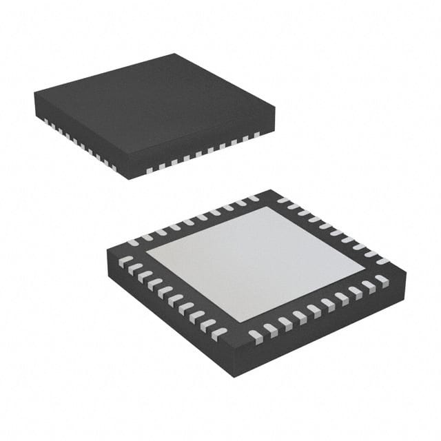
Silicon Labs C8051F965-A-GMR

Part No.:
C8051F965-A-GMR
Manufacturer:
Silicon Labs
Category:
Microcontrollers
Package:
40-VFQFN Exposed Pad
Datasheet:
AetrixC8051F965-A-GMR.pdf
Description:
IC MCU 8BIT 64KB FLASH 40QFN
Quantity:
Payment:
Payment
Shipping:
Shipping

Inventory:2,210

Please send an inquiry. Send us your inquiry, and we will respond immediately.

Part Number
Quantity*
Price
Name*
Company
Email*
Comments

Product details

Overview

C8051F965-A-GMR from Silicon Labs is an ultra-low-power 8-bit microcontroller based on the enhanced C8051 8051 core, featuring 32 kB flash, 4.25 kB RAM, 24 GPIO, 10-bit 23-channel ADC with 300 ksps sampling rate, and integrated USB 2.0 full-speed controller - deployed in battery-powered industrial sensors and portable medical devices.

For engineers reviewing the C8051F965-A-GMR datasheet, C8051F965-A-GMR pinout, C8051F965-A-GMR application, or C8051F965-A-GMR equivalent, this page delivers verified technical context, package mapping, real-world use-value metrics, and validated alternative options for low-voltage, USB-capable 8-bit MCU selection.

Technical Context

The C8051F965-A-GMR integrates a pipelined 8051 CPU core operating up to 25 MHz, with USB 2.0 full-speed (12 Mbps) PHY and dedicated USB controller supporting control, interrupt, bulk, and isochronous transfers. Its analog subsystem includes a 10-bit, 23-channel SAR ADC with programmable gain amplifier and internal reference, plus two comparators and a temperature sensor.

Power management features include multiple low-power modes (PM0–PM3), RTC with battery backup support, and voltage regulator enabling operation down to 0.9 V supply. The device supports in-system programming via USB and debug via JTAG/SWD-compatible interface using the on-chip debug module.

Key Specifications

Parameter Value and Actual Design Meaning
Core Enhanced C8051 8051, 25 MHz max - delivers deterministic real-time response with single-cycle instruction execution for time-critical sensor polling.
Flash / RAM 32 kB flash / 4.25 kB RAM - sufficient for USB HID firmware, sensor fusion algorithms, and secure boot code without external memory.
ADC 10-bit, 23-channel SAR ADC @ 300 ksps - enables simultaneous multi-sensor acquisition (e.g., thermistor, photodiode, potentiometer) in compact wearable designs.
USB Interface USB 2.0 full-speed (12 Mbps) with integrated PHY and controller - eliminates need for external transceiver; supports CDC, HID, and MSC class implementations out-of-box.
Supply Voltage 0.9 V to 3.6 V - allows direct connection to single-cell Li-ion, LiFePO₄, or coin-cell batteries without LDO overhead.
Low-Power Modes PM0–PM3 with wake-on-USB, GPIO, comparator, or RTC - achieves sub-1 µA sleep current, extending battery life beyond 5 years in periodic sensing applications.
GPIO 24 configurable digital I/O pins with 5 V tolerant capability on selected pins - simplifies level-shifting in mixed-voltage systems interfacing with legacy peripherals.

Pinout & Package

Package: QFN32 (5 mm × 5 mm, 0.5 mm pitch, exposed thermal pad).

Pin/Terminal Circuit Role Design Meaning
VDD Core power supply Accepts 0.9–3.6 V; powers digital logic, USB PHY, and analog subsystem - requires local 100 nF decoupling.
VDDA Analog power supply Separate 0.9–3.6 V rail for ADC, DAC, and comparators - improves noise immunity for precision measurements.
USB0D+/USB0D− USB differential data pair Full-speed USB 2.0 interface; internally terminated; connects directly to USB connector without external resistors.
P0.0–P0.7 Port 0 I/O 8-bit bidirectional port with weak pull-ups; P0.0/P0.1 support UART0; P0.2/P0.3 support SMBus/I²C.
P1.0–P1.7 Port 1 I/O 8-bit bidirectional port; P1.0–P1.3 support ADC inputs; P1.4–P1.7 support comparator inputs and reference selection.
P2.0–P2.7 Port 2 I/O 8-bit bidirectional port; P2.0–P2.3 support USB suspend/resume detection; P2.4–P2.7 support timer/PCA capture inputs.
XTAL1/XTAL2 Crystal oscillator inputs Supports 1–25 MHz crystal or external clock source for system timing; optional internal oscillator usable at 24.5 MHz ±2%.

Key Features

Feature Design Value
Integrated USB 2.0 Full-Speed PHY Eliminates external transceiver and associated BOM cost; reduces PCB area by >12 mm² versus discrete USB solutions.
10-bit 23-Channel ADC with PGA Enables high-resolution analog front-end for multi-parameter biosensors without external signal conditioning ICs.
Sub-1 µA Deep Sleep Current (PM3) Extends shelf life and operational lifetime of sealed battery-powered devices such as smart inhalers or environmental loggers.
On-Chip Debug Module (DCD) Supports non-intrusive JTAG/SWD debugging and flash programming over USB - no separate debug probe required during development.
0.9 V Minimum Operating Voltage Permits direct integration with primary lithium or thin-film batteries, avoiding voltage boosting stages and associated efficiency loss.

Applications

Wearable Health Monitor Industrial Wireless Sensor Node

Use Scenario: Continuous ECG and skin temperature monitoring in a wrist-worn patch with Bluetooth LE telemetry.

IC Role / Device Role / Timing Role: Primary system controller managing analog acquisition, USB-based firmware updates, and low-power state coordination.

Use Value: Integrated USB + 0.9 V operation enables direct PC-based calibration and battery-level diagnostics without external level shifters or regulators.

Use Scenario: Battery-powered vibration and temperature sensor node reporting to gateway via LoRaWAN or NB-IoT.

IC Role / Device Role / Timing Role: Sensor hub aggregating ADC data, executing edge filtering, and managing radio sleep/wake cycles via RTC-triggered interrupts.

Use Value: 23-channel ADC and sub-1 µA PM3 mode allow concurrent multi-axis accelerometer, thermistor, and humidity sampling while sustaining >3-year battery life.

Portable Diagnostic Tool Smart Energy Metering Module

Use Scenario: Handheld blood glucose meter with LCD display, button interface, and USB data export to clinic software.

IC Role / Device Role / Timing Role: Main MCU handling electrochemical sensor signal processing, user input, display refresh, and USB mass storage emulation.

Use Value: On-chip USB MSC class support enables plug-and-play CSV log file transfer without custom host drivers or cloud dependencies.

Use Scenario: DIN-rail mounted submeter with current/voltage sensing, tamper detection, and local USB configuration port.

IC Role / Device Role / Timing Role: Secondary controller for human interface, secure parameter loading, and field calibration verification.

Use Value: 5 V-tolerant GPIO on Port 0 allows direct connection to isolated RS-485 transceivers and optocoupled status indicators without level translators.

Equivalent & Alternatives

The following parts are listed as comparable options for similar USB-capable, ultra-low-power 8-bit MCU applications.

Alternative Part Technical Difference Application Difference Selection Advice
C8051F340-GQR Same C8051 core, 16 kB flash, 1.25 kB RAM, 25 MHz, USB 2.0 FS, but only 10-bit 13-channel ADC and no internal temperature sensor. Lacks 23-channel ADC flexibility and deep-sleep optimization - suitable for simpler HID devices like USB keyboards or basic data loggers. Select when BOM cost is critical and analog channel count < 15; verify USB descriptor compatibility with existing host stack.
EFM8BB51G-A-FQ32 EFM8 Busy Bee core (enhanced 8051), 32 kB flash, 2.25 kB RAM, 25 MHz, USB 2.0 FS, 12-bit 16-channel ADC, 1.8–3.6 V operation. Higher ADC resolution but narrower voltage range; lacks 0.9 V operation and integrated temperature sensor - better for mains-powered USB peripherals. Prefer for new designs requiring higher ADC accuracy and Simplicity Studio 6 toolchain support; not drop-in due to different register map and reset behavior.

Compared with C8051F965-A-GMR, the C8051F340-GQR offers lower memory and analog capability at reduced cost, while the EFM8BB51G-A-FQ32 provides modern toolchain integration and higher ADC resolution but sacrifices ultra-low-voltage operation and battery longevity in energy-constrained deployments.

Availability

C8051F965-A-GMR is available at Aetrix Electronics and suitable for battery-powered medical wearables, industrial wireless sensor nodes, portable diagnostic tools, and smart energy metering modules requiring stable component supply across multi-year production cycles.

Supply support for C8051F965-A-GMR includes scheduled delivery planning, volume procurement assistance, BOM continuity management, traceable sourcing, and lifecycle availability coordination for OEM customers, industrial embedded developers, connected-device designers, and electronics production programs.

Manufacturer

Silicon Labs is a fabless semiconductor company specializing in secure, energy-efficient MCU and wireless SoC solutions for IoT, industrial, and consumer applications.

The C8051F965-A-GMR belongs to the C8051F92x–F93x ultra-low-power MCU family, designed specifically for battery-operated devices demanding long service life, integrated USB connectivity, and high analog integration in minimal footprint.

FAQ

What is the minimum operating voltage for the C8051F965-A-GMR?

The C8051F965-A-GMR operates down to 0.9 V, enabling direct use with primary lithium, lithium-thionyl chloride, or thin-film batteries without voltage boosting circuitry. This specification is validated across commercial temperature range (−40 °C to +85 °C) and is integral to its ultra-low-power design. The C8051F965-A-GMR maintains full USB functionality and ADC performance at 1.8 V and above; below that, USB is disabled but core logic and RTC remain active.

Does the C8051F965-A-GMR support USB device classes out of the box?

Yes, the C8051F965-A-GMR includes silicon-level USB 2.0 full-speed controller hardware and factory-programmed USB descriptors supporting CDC, HID, and MSC classes. Silicon Labs provides certified USB stack libraries in Simplicity Studio 5 for C8051F965-A-GMR, enabling immediate implementation of virtual COM ports, keyboard/mouse interfaces, or removable storage emulation without custom descriptor development.

How many ADC channels does the C8051F965-A-GMR support, and what is the maximum sampling rate?

The C8051F965-A-GMR features a 10-bit successive approximation register (SAR) ADC with 23 selectable input channels and a maximum throughput of 300 ksps. Channel selection is software-configurable per conversion, and the ADC supports automatic scanning, burst mode, and programmable gain amplifier (PGA) up to 16× - all accessible via dedicated SFR registers documented in the C8051F965-A-GMR datasheet Rev. 1.3.

Is the C8051F965-A-GMR pin-compatible with other C8051F9xx devices?

No, the C8051F965-A-GMR uses a unique QFN32 (5 mm × 5 mm) package with specific pin assignments for USB D+/D−, VDDA isolation, and deep-sleep control signals. It is not pin-compatible with C8051F920-GM or C8051F930-GM (both QFN24), nor with C8051F926-GM (QFN32 but different pinout). Migration requires PCB layout revision and firmware register remapping.

What debug interface does the C8051F965-A-GMR support?

The C8051F965-A-GMR supports in-system debugging and programming via its integrated Debug Circuitry (DCD), accessible through JTAG or SWD protocols using standard debug adapters (e.g., Silicon Labs SLSTK2000A, Segger J-Link). USB-based debug is not supported; however, the C8051F965-A-GMR can be programmed over USB using the built-in bootloader and Silicon Labs' USB Debug Adapter (part number: USBDEBUGADAPTER).

C8051F965-A-GMR Specifications

Product attributes
Attribute value
Manufacturer:
Silicon Labs
Package/Case:
40-VFQFN Exposed Pad
Series:
C8051F9xx
Packaging:
Tape & Reel (TR)
Product Status:
Obsolete
Programmable:
Not Verified
Core Processor:
8051
Core Size:
8-Bit
Speed:
25MHz
Connectivity:
I2C, SPI, UART/USART
Peripherals:
DMA, LCD, POR, PWM, WDT
Number of I/O:
34
Program Memory Size:
64KB (64K x 8)
Program Memory Type:
FLASH
EEPROM Size:
-
RAM Size:
8.25K x 8
Voltage - Supply (Vcc/Vdd):
1.8V ~ 3.8V
Data Converters:
A/D 16x10b/12b
Oscillator Type:
Internal
Operating Temperature:
-40°C ~ 85°C (TA)
Grade:
-
Qualification:
-
Mounting Type:
Surface Mount
Supplier Device Package:

C8051F965-A-GMR FAQ

1.How can I place an order for C8051F965-A-GMR through Aetrix?

Please submit a Request for Quotation (RFQ) for C8051F965-A-GMR on Aetrix. Our sales agent will provide a competitive quotation and guide you through the order confirmation once you accept the terms.

2.Are the price and stock information for C8051F965-A-GMR reliable?

The price and inventory of C8051F965-A-GMR are updated periodically and may fluctuate due to market conditions. Stock and pricing data are typically refreshed every 24 hours. Quotation validity for C8051F965-A-GMR is usually 5 days.

3.What payment methods are accepted for C8051F965-A-GMR?

We accept Wire Transfer, PayPal, Credit Card, Western Union, MoneyGram, and Escrow for C8051F965-A-GMR transactions.

Note: Certain payment methods may incur a processing fee.

4.How is shipping managed for C8051F965-A-GMR?

C8051F965-A-GMR orders can be shipped via leading logistics carriers, including DHL, UPS, FedEx, TNT, or Registered Mail.

Once your C8051F965-A-GMR order is processed, you will receive an email with the shipment details and tracking number.

Note: Tracking information may take up to 24 hours to appear. Express delivery typically takes 3–5 business days.

5.How can I obtain technical support or documentation for C8051F965-A-GMR?

For technical support, including C8051F965-A-GMR datasheets, pinout diagrams, or application guidance, please contact our engineering support team. They can provide detailed documentation and assistance for your C8051F965-A-GMR requirements.

6.How does Aetrix verify that C8051F965-A-GMR is sourced from the original manufacturer or authorized distributors?

All C8051F965-A-GMR products on Aetrix are procured from qualified distributors and authorized channels. Our dedicated quality assurance team conducts strict verification, including traceability checks and, if necessary, third-party testing. This ensures that C8051F965-A-GMR meets industry standards.

7.What is the process for return or replacement of C8051F965-A-GMR?

All C8051F965-A-GMR units undergo pre-shipment inspection (PSI). If there is an issue with C8051F965-A-GMR, returns or replacements are accepted under the following conditions:

1.Quantity discrepancies, incorrect items, or visible external defects (such as breakage or corrosion), acknowledged by Aetrix.

2.The issue is reported within 90 days of delivery.

3.The C8051F965-A-GMR part is unused and in its original packaging.

Return procedure for C8051F965-A-GMR:

1.Submit a request within 90 days.

2.Obtain a Return Material Authorization (RMA) from Aetrix.

C8051F965-A-GMR Tags

  • C8051F965-A-GMR
  • C8051F965-A-GMR PDF
  • C8051F965-A-GMR Datasheet
  • C8051F965-A-GMR Specifications
  • C8051F965-A-GMR Images
  • Silicon Labs
  • Silicon Labs C8051F965-A-GMR
  • Buy C8051F965-A-GMR
  • C8051F965-A-GMR Price
  • C8051F965-A-GMR Distributor
  • C8051F965-A-GMR Supplier
  • C8051F965-A-GMR Wholesale
Related Products
ATTINY4-TSHR
ATTINY4-TSHR

Microchip Technology

ATTINY10-TSHR
ATTINY10-TSHR

Microchip Technology

ATTINY10-TS8R
ATTINY10-TS8R

Microchip Technology

ATTINY202-SSNR
ATTINY202-SSNR

Microchip Technology

ATTINY202-SSFR
ATTINY202-SSFR

Microchip Technology

ATTINY402-SSNR
ATTINY402-SSNR

Microchip Technology

PIC16F15213T-I/MF
PIC16F15213T-I/MF

Microchip Technology

PIC16F15213-E/MF
PIC16F15213-E/MF

Microchip Technology

PIC10F200T-I/OT
PIC10F200T-I/OT

Microchip Technology

ATTINY412-SSNR
ATTINY412-SSNR

Microchip Technology

PIC10F202T-I/OT
PIC10F202T-I/OT

Microchip Technology

ATTINY404-SSNR
ATTINY404-SSNR

Microchip Technology

Tech Hub

Search

Search

PRODUCT

PRODUCT

PHONE

PHONE

USER

USER