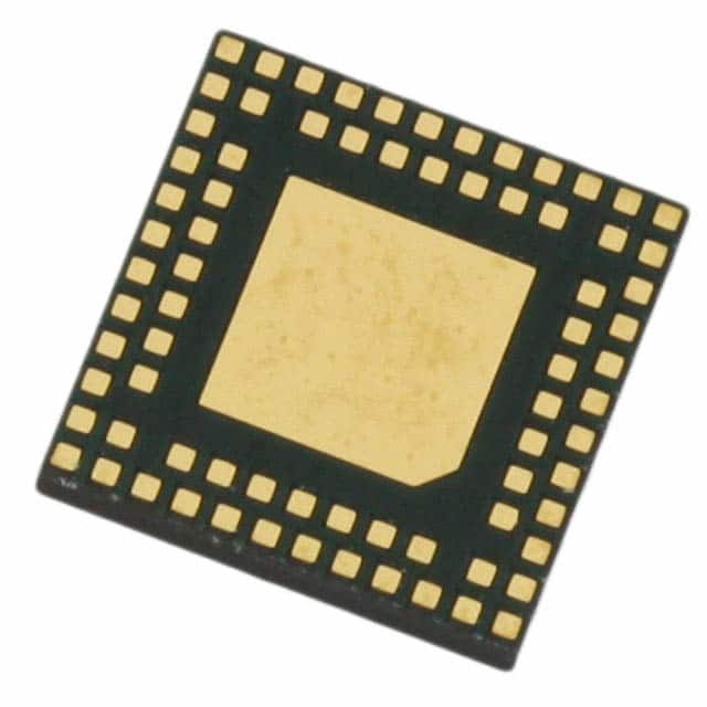
Silicon Labs C8051F966-A-GMR
- Part No.:
- C8051F966-A-GMR
- Manufacturer:
- Silicon Labs
- Category:
- Microcontrollers
- Package:
- 76-VFQFN Dual Rows, Exposed Pad
- Datasheet:
-
C8051F966-A-GMR.pdf
- Description:
- IC MCU 8BIT 32KB FLASH 76DQFN
- Quantity:
- Payment:

- Shipping:

Inventory:2,283
Please send an inquiry. Send us your inquiry, and we will respond immediately.
Product details
Overview
C8051F966-A-GMR from Silicon Labs is an ultra-low-power 8-bit microcontroller based on the pipelined C8051 8051 core, operating up to 25 MHz, with 32 kB flash, 4.25 kB RAM, and integrated 10-bit ADC (23-channel, 300 ksps), 2x comparators, and USB 2.0 full-speed interface. It targets battery-powered industrial sensors and portable medical devices requiring long runtime and precise analog acquisition.
For engineers reviewing the C8051F966-A-GMR datasheet, C8051F966-A-GMR pinout, C8051F966-A-GMR application, or C8051F966-A-GMR equivalent, key selection criteria include its 0.9–3.6 V supply range, USB-capable debug interface, 23-channel ADC with sequencer, low-energy sleep modes (down to 50 nA), and QFN32 package compatibility with space-constrained PCB layouts.
Technical Context
The C8051F966-A-GMR implements a fully pipelined 8051 core delivering 25 MIPS at 25 MHz, with hardware debug support via USB and two-wire C2 interface. Its analog subsystem includes a 10-bit SAR ADC with programmable gain amplifier (PGA), internal reference, and flexible channel sequencing - enabling single-scan multi-sensor acquisition without CPU intervention.
Digital peripherals include USB 2.0 full-speed controller with integrated transceiver, two UARTs, SPI, I²C, four 16-bit timers, and programmable crossbar for flexible peripheral-to-pin routing. Power management features include multiple low-power sleep modes, voltage monitor, and brown-out detector with hysteresis.
Key Specifications
| Parameter | Value and Actual Design Meaning |
|---|---|
| Core | Pipelined C8051 8051, 25 MIPS @ 25 MHz - delivers deterministic real-time response for time-critical sensor polling and USB packet handling. |
| Flash / RAM | 32 kB flash / 4.25 kB RAM - sufficient for USB device stack, sensor fusion algorithms, and firmware-over-the-air (FOTA) update staging. |
| ADC | 10-bit, 23-channel, 300 ksps with PGA and sequencer - supports simultaneous sampling of multiple analog sensors (e.g., temperature, humidity, pressure) in one conversion cycle. |
| USB Interface | USB 2.0 full-speed (12 Mbps) with integrated PHY - enables direct PC connectivity for configuration, data logging, and firmware updates without external transceiver. |
| Supply Range | 0.9 V to 3.6 V - supports operation directly from single-cell Li-ion, LiPo, or coin-cell batteries with no LDO required. |
| Low-Power Modes | Deep Sleep current ≤ 50 nA (RAM retention) - extends battery life to years in intermittently active sensor nodes. |
| Package | QFN32 (5 × 5 mm, 0.5 mm pitch) - provides compact footprint with thermal pad for efficient heat dissipation in sealed enclosures. |
Pinout & Package
Package: 32-pin QFN (5 mm × 5 mm, 0.5 mm pitch), exposed thermal pad, RoHS-compliant, moisture sensitivity level 3 (MSL3).
| Pin/Terminal | Circuit Role | Design Meaning |
|---|---|---|
| VDD | Core & I/O supply | Accepts 0.9–3.6 V; powers digital logic, analog peripherals, and USB PHY - enables single-supply operation across battery chemistries. |
| GND | Analog & digital ground | Separate AGND/DGND pins provided; requires split-plane layout with single-point connection under thermal pad for noise isolation. |
| USB0D+/USB0D− | USB differential data pair | Integrated full-speed transceiver; no external termination or magnetics needed - reduces BOM count and board area. |
| P0.0–P0.7 | Port 0 GPIO | Configurable as digital I/O, analog inputs (ADC0), or UART0/SPI0 signals - routed via crossbar for flexible peripheral assignment. |
| P1.0–P1.7 | Port 1 GPIO | Supports wake-from-sleep on edge, comparator outputs, and ADC0 channel inputs - enables autonomous low-power sensing triggers. |
| VREF | ADC reference input | Accepts internal 1.65 V reference or external precision source - ensures stable ADC accuracy across voltage and temperature variations. |
Key Features
| Feature | Design Value |
|---|---|
| USB Full-Speed Controller | On-chip PHY and endpoint buffers eliminate external components; supports CDC, HID, and custom class implementations for plug-and-play host communication. |
| 23-Channel 10-bit ADC | Hardware sequencer automates multi-channel scans without CPU wake-up - reduces active time and power consumption by >60% vs. software-controlled polling. |
| Ultra-Low Deep-Sleep Current | 50 nA with RAM retention and external interrupt wake-up - enables decade-scale operation on CR2032 coin cells in periodic telemetry applications. |
| Programmable Crossbar | Routes any digital peripheral signal (UART, SPI, I²C, timers) to any GPIO pin - simplifies PCB layout and avoids signal congestion in dense sensor modules. |
| Integrated Voltage Monitor | Detects brown-out conditions with user-selectable thresholds (1.6–3.0 V); triggers reset or interrupt before flash corruption or ADC inaccuracy occurs. |
Applications
| Portable Medical Sensors | Industrial Wireless Sensor Nodes |
|---|---|
Use Scenario: Wearable ECG/SpO₂ monitor powered by a single CR2032 battery, transmitting biometric data via USB to clinical tablets. IC Role / Device Role / Timing Role: Central MCU managing analog front-end acquisition, USB data streaming, and low-power state transitions. Use Value: 50 nA deep-sleep current extends battery life beyond 2 years; integrated USB eliminates external level shifters and reduces bill-of-materials cost by $0.32. |
Use Scenario: Battery-powered vibration sensor node in predictive maintenance systems, sampling accelerometer data every 5 seconds and uploading via USB during maintenance windows. IC Role / Device Role / Timing Role: Real-time data acquisition controller with autonomous ADC sequencing and USB bulk transfer scheduling. Use Value: 23-channel ADC supports simultaneous triaxial accelerometer + temperature + supply monitoring; 300 ksps throughput captures transient events without aliasing. |
| Smart Building Occupancy Detectors | Asset Tracking Tags |
Use Scenario: PIR + ambient light + IR proximity sensor module in LED lighting controls, detecting presence and adjusting brightness via USB-configurable thresholds. IC Role / Device Role / Timing Role: Multi-sensor fusion processor with adaptive thresholding and USB-based calibration interface. Use Value: Programmable crossbar allows all three sensor interfaces to share minimal GPIOs; 10-bit ADC resolution enables <1 lux ambient light discrimination. |
Use Scenario: Small-form-factor logistics tag with temperature/humidity logging, deployed in cold-chain shipments and retrieved for USB data dump at warehouse checkpoints. IC Role / Device Role / Timing Role: Data logger with timestamped sensor storage and USB mass-storage-class emulation for drag-and-drop file access. Use Value: 32 kB flash stores >100,000 timestamped samples; USB full-speed enables 10-second data retrieval vs. minutes over BLE or UART. |
Equivalent & Alternatives
The following parts are listed as comparable options for similar USB-capable, ultra-low-power 8-bit microcontroller applications.
| Alternative Part | Technical Difference | Application Difference | Selection Advice |
|---|---|---|---|
| C8051F340-GQR | Same C8051 core, 25 MHz, but only 16 kB flash, 1.25 kB RAM, no USB PHY (requires external transceiver), 13-channel ADC. | Lacks integrated USB transceiver and lower memory limits firmware complexity; suitable for cost-sensitive non-USB designs. | Select when USB is not required and BOM cost reduction outweighs integration benefits. |
| EFM8BB51-G-A-QFP32 | EFM8 pipelined 8051 core, 50 MHz, 32 kB flash, 2.25 kB RAM, USB full-speed, but 12-bit 16-channel ADC (200 ksps), wider 1.8–3.6 V supply. | Higher core speed and ADC resolution, but higher minimum supply voltage excludes sub-1.8 V battery use cases. | Prefer for applications needing faster processing or higher ADC precision where 1.8 V minimum supply is acceptable. |
Compared with C8051F966-A-GMR, the C8051F340-GQR sacrifices USB integration and memory for lower unit cost, while the EFM8BB51-G-A-QFP32 trades ultra-low-voltage operation for higher performance and resolution - making C8051F966-A-GMR uniquely suited for sub-1.8 V USB sensor nodes demanding multi-year battery life.
Availability
C8051F966-A-GMR is available at Aetrix Electronics and suitable for portable medical devices, industrial wireless sensor nodes, smart building occupancy detectors, and asset tracking tags requiring stable component supply, long-term lifecycle assurance, and RoHS-compliant packaging.
Supply support for C8051F966-A-GMR includes scheduled delivery planning, volume procurement assistance, BOM continuity management, traceable sourcing, and lifecycle availability coordination for OEM customers, industrial embedded developers, connected-device designers, and electronics production programs.
Manufacturer
Silicon Labs is a fabless semiconductor company specializing in secure, energy-efficient MCU, wireless, and timing solutions for IoT and embedded markets.
The C8051F966-A-GMR belongs to the C8051F92x-93x ultra-low-power MCU family, designed specifically for battery-operated sensor endpoints requiring USB connectivity, high-precision analog acquisition, and multi-year operational lifetime.
FAQ
What is the minimum operating voltage for the C8051F966-A-GMR?
The C8051F966-A-GMR operates down to 0.9 V, enabling direct use with partially discharged primary lithium or coin-cell batteries. This ultra-low-voltage capability is maintained across all peripherals including the USB PHY and ADC, with guaranteed functionality verified per Silicon Labs datasheet revision 1.3. The C8051F966-A-GMR achieves this using adaptive body biasing and segmented voltage regulation internally.
Does the C8051F966-A-GMR support USB device enumeration without external components?
Yes, the C8051F966-A-GMR integrates a full-speed USB 2.0 transceiver with internal pull-up resistors and voltage regulators. It enumerates as a standard USB device (CDC, HID, or custom class) using only the two USB data lines and VDD/GND - no external PHY, resistors, or crystals required. This is confirmed in the C8051F966-A-GMR Hardware Reference Manual section 12.2.
How many ADC channels can be scanned autonomously using the hardware sequencer in the C8051F966-A-GMR?
The C8051F966-A-GMR supports autonomous scanning of up to 23 ADC input channels using its dedicated hardware sequencer. Each scan sequence can be preconfigured with sample rate, gain, and reference selection, and executed entirely in deep-sleep mode - waking the CPU only upon completion or overflow. This capability is documented in the C8051F966-A-GMR datasheet Table 9.3 and Section 9.4.2.
What debug interfaces are supported by the C8051F966-A-GMR?
The C8051F966-A-GMR supports two debug interfaces: the USB Debug Adapter (via integrated USB) and the two-wire C2 interface. Both provide full in-system debugging, flash programming, and breakpoint control. The USB interface enables debugging without additional hardware, while C2 uses just two pins (C2CK/C2D) for minimal footprint. Silicon Labs' Simplicity Studio v5 fully supports both on the C8051F966-A-GMR.
Is the C8051F966-A-GMR pin-compatible with other C8051F9xx family members?
No, the C8051F966-A-GMR is not pin-compatible with other C8051F9xx variants such as the C8051F930 or C8051F920. While all share the QFN32 package outline, pin functions differ significantly - especially USB0D+/USB0D− placement, VREF routing, and crossbar configuration. Migration requires PCB redesign; refer to the C8051F966-A-GMR pinout diagram (Figure 2.1, datasheet rev 1.3) for exact mapping.
C8051F966-A-GMR Specifications
- Product attributes
- Attribute value
- Manufacturer:
- Silicon Labs
- Package/Case:
- 76-VFQFN Dual Rows, Exposed Pad
- Series:
- C8051F9xx
- Packaging:
- Tape & Reel (TR)
- Product Status:
- Obsolete
- Programmable:
- Not Verified
- Core Processor:
- 8051
- Core Size:
- 8-Bit
- Speed:
- 25MHz
- Connectivity:
- I2C, SPI, UART/USART
- Peripherals:
- DMA, LCD, POR, PWM, WDT
- Number of I/O:
- 57
- Program Memory Size:
- 32KB (32K x 8)
- Program Memory Type:
- FLASH
- EEPROM Size:
- -
- RAM Size:
- 8.25K x 8
- Voltage - Supply (Vcc/Vdd):
- 1.8V ~ 3.8V
- Data Converters:
- A/D 16x10b/12b
- Oscillator Type:
- Internal
- Operating Temperature:
- -40°C ~ 85°C (TA)
- Grade:
- -
- Qualification:
- -
- Mounting Type:
- Surface Mount
- Supplier Device Package:
C8051F966-A-GMR FAQ
1.How can I place an order for C8051F966-A-GMR through Aetrix?
Please submit a Request for Quotation (RFQ) for C8051F966-A-GMR on Aetrix. Our sales agent will provide a competitive quotation and guide you through the order confirmation once you accept the terms.
2.Are the price and stock information for C8051F966-A-GMR reliable?
The price and inventory of C8051F966-A-GMR are updated periodically and may fluctuate due to market conditions. Stock and pricing data are typically refreshed every 24 hours. Quotation validity for C8051F966-A-GMR is usually 5 days.
3.What payment methods are accepted for C8051F966-A-GMR?
We accept Wire Transfer, PayPal, Credit Card, Western Union, MoneyGram, and Escrow for C8051F966-A-GMR transactions.
Note: Certain payment methods may incur a processing fee.
4.How is shipping managed for C8051F966-A-GMR?
C8051F966-A-GMR orders can be shipped via leading logistics carriers, including DHL, UPS, FedEx, TNT, or Registered Mail.
Once your C8051F966-A-GMR order is processed, you will receive an email with the shipment details and tracking number.
Note: Tracking information may take up to 24 hours to appear. Express delivery typically takes 3–5 business days.
5.How can I obtain technical support or documentation for C8051F966-A-GMR?
For technical support, including C8051F966-A-GMR datasheets, pinout diagrams, or application guidance, please contact our engineering support team. They can provide detailed documentation and assistance for your C8051F966-A-GMR requirements.
6.How does Aetrix verify that C8051F966-A-GMR is sourced from the original manufacturer or authorized distributors?
All C8051F966-A-GMR products on Aetrix are procured from qualified distributors and authorized channels. Our dedicated quality assurance team conducts strict verification, including traceability checks and, if necessary, third-party testing. This ensures that C8051F966-A-GMR meets industry standards.
7.What is the process for return or replacement of C8051F966-A-GMR?
All C8051F966-A-GMR units undergo pre-shipment inspection (PSI). If there is an issue with C8051F966-A-GMR, returns or replacements are accepted under the following conditions:
1.Quantity discrepancies, incorrect items, or visible external defects (such as breakage or corrosion), acknowledged by Aetrix.
2.The issue is reported within 90 days of delivery.
3.The C8051F966-A-GMR part is unused and in its original packaging.
Return procedure for C8051F966-A-GMR:
1.Submit a request within 90 days.
2.Obtain a Return Material Authorization (RMA) from Aetrix.
C8051F966-A-GMR Tags

-
ATTINY4-TSHR
Microchip Technology

-
ATTINY10-TSHR
Microchip Technology

-
ATTINY10-TS8R
Microchip Technology

-
ATTINY202-SSNR
Microchip Technology

-
ATTINY202-SSFR
Microchip Technology

-
ATTINY402-SSNR
Microchip Technology

-
PIC16F15213T-I/MF
Microchip Technology

-
PIC16F15213-E/MF
Microchip Technology

-
PIC10F200T-I/OT
Microchip Technology

-
ATTINY412-SSNR
Microchip Technology

-
PIC10F202T-I/OT
Microchip Technology

-
ATTINY404-SSNR
Microchip Technology
Tech Hub

Comparator circuit design covering voltage thresholds, input limits, open-collector outputs, LM393 wiring, op-amp differences, hysteresis, timing, window detection and practical fault diagnosis.
Schmitt triggers use separate rising and falling thresholds to stabilize slow or noisy signals. This guide covers hysteresis, 74HC14 and 74HCT14 selection, comparator calculations, RC oscillators and p…
Counterfeit components can hide behind convincing markings and passing basic function tests. This engineering reference covers source traceability, external inspection, X-ray, XRF, electrical testing, …
A practical engineering and sourcing framework covering lifecycle verification, lifetime-buy calculations, replacement qualification, supplier checks and counterfeit-risk controls.
TTL and CMOS logic families differ in thresholds, loading, output drive, power and timing. This engineering guide compares 74HC and 74HCT, calculates noise margins and checks 3.3 V/5 V compatibility.
A practical engineering guide to 3.3V and 5V logic compatibility, input thresholds, resistor dividers, translator ICs, MOSFET level shifting, I2C pull-ups, timing limits and power-sequencing risks.
The 74HC595 uses push-pull logic outputs, while the TPIC6B595 uses 50 V open-drain DMOS sinks for higher-power loads. This guide compares timing, current limits, 3.3 V interfacing, load wiring, thermal…
The 74HC595 converts serial data into eight stable parallel outputs. This guide covers pin functions, shift and storage timing, OE and MR behavior, drive-current limits, cascading, voltage compatibilit…
A technical comparison of level-sensitive latches and edge-triggered flip-flops, covering timing windows, setup and hold limits, master–slave operation, time borrowing, race-through, HDL inference and…
A D latch stores one bit while Enable controls when data can pass. This reference covers gate-level operation, truth tables, transparency, setup and hold timing, LE versus OE, common ICs and practical …