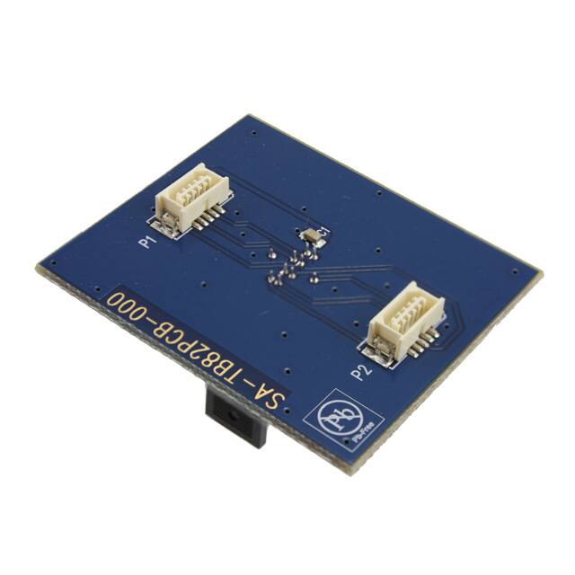
Silicon Labs C8051T606ZDB
- Part No.:
- C8051T606ZDB
- Manufacturer:
- Silicon Labs
- Category:
- Programming Adapters, Sockets
- Package:
- Datasheet:
-
C8051T606ZDB.pdf
- Description:
- CARD DAUGHTER QFN10 SOCKET
- Quantity:
- Payment:

- Shipping:

Inventory:4,752
Please send an inquiry. Send us your inquiry, and we will respond immediately.
Product details
Overview
C8051T606ZDB from Silicon Laboratories is a mixed-signal, byte-programmable EPROM microcontroller featuring an enhanced 8051 core, 1.5 kB on-chip EPROM, 128 bytes RAM, 2×16-bit timers, PCA with PWM and capture/compare, hardware SMBus and UART, and 8-port I/O. It operates from 1.8–3.6 V, supports –40 to +85 °C, and targets compact sensor interface and low-power embedded control.
For engineers reviewing the C8051T606ZDB datasheet, C8051T606ZDB pinout, C8051T606ZDB application, or C8051T606ZDB equivalent, key selection criteria include its QFN10 package, absence of integrated ADC (unlike T600/T602/T604), MSOP10/SOIC14-compatible pin mapping, and support for crystal-less UART via ±2% internal oscillator.
Technical Context
The C8051T606ZDB implements the CIP-51 8051-compatible core with pipelined execution-70% of instructions complete in 1–2 system clocks-and delivers up to 25 MIPS at 25 MHz. Its digital peripheral set includes three 16-bit counter/timers, a programmable counter array (PCA) supporting 8/16-bit PWM, edge-triggered capture, frequency output, and watchdog timer mode.
Power management includes Idle and Stop modes; supply regulation uses an on-chip LDO with VDD monitor reset and missing-clock detector. The device lacks the 10-bit ADC and temperature sensor found in T600/T602/T604 variants, confirming its role as a cost-optimized, analog-minimized MCU variant within the T60x family.
Key Specifications
| Parameter | Value and Actual Design Meaning |
|---|---|
| Core | Enhanced 8051 (CIP-51); executes most instructions in 1–2 clocks for deterministic real-time response |
| EPROM Size | 1.5 kB byte-programmable EPROM; enables field updates without external memory |
| RAM | 128 bytes internal data RAM; sufficient for small control stacks and peripheral register buffering |
| Max Clock | 25 MHz system clock; supports 25 MIPS throughput for time-critical firmware loops |
| Supply Range | 1.8–3.6 V; compatible with single-cell Li-ion, coin cell, or regulated 3.3 V rails |
| Temp Range | –40 to +85 °C; qualified for industrial and automotive under-hood ambient environments |
| I/O Pins | 8 programmable port pins with high sink current; drives LEDs, relays, or logic-level MOSFETs directly |
| Serial Interfaces | Hardware UART0 and SMBus™; enables sensor networking and host communication without bit-banging |
Pinout & Package
Package: 2 × 2 mm, 10-pin QFN (ZDB suffix per ordering guide). Exposed thermal pad improves power dissipation in space-constrained PCB layouts.
| Pin/Terminal | Circuit Role | Design Meaning |
|---|---|---|
| VDD | Core & I/O supply | 1.8–3.6 V input; powers all digital logic and I/O drivers |
| GND | Ground reference | Common return path for analog and digital sections; must be low-impedance |
| P0.0 / CEX0 | Port 0.0 / PCA Channel 0 | Digital I/O or PCA capture/compare output; supports PWM generation or event timing |
| P0.1 / CEX1 | Port 0.1 / PCA Channel 1 | Digital I/O or PCA capture/compare output; enables dual-channel PWM or frequency measurement |
| P0.2 / TX0 | Port 0.2 / UART0 TX | UART transmit output; drives RS-232 level shifters or 3.3 V logic receivers |
| P0.3 / RX0 | Port 0.3 / UART0 RX | UART receive input; accepts TTL/CMOS-level serial data |
| P0.4 / SCL | Port 0.4 / SMBus Clock | SMBus clock line; open-drain output with internal pull-up; requires external pull-up for bus operation |
| P0.5 / SDA | Port 0.5 / SMBus Data | SMBus data line; open-drain output with internal pull-up; shares bidirectional bus arbitration |
| C2CK / XTAL2 | C2 debug clock / ext. oscillator | Shared pin for C2 programming clock or external crystal/capacitor connection |
| C2D / XTAL1 | C2 debug data / ext. oscillator | Shared pin for C2 bidirectional debug I/O or external oscillator input |
Key Features
| Feature | Design Value |
|---|---|
| Crystal-less UART operation | Internal 24.5 MHz oscillator with ±2% accuracy eliminates need for external crystal in UART applications |
| On-chip LDO regulator | Stabilizes core voltage across VDD variation; enables stable operation from unregulated battery sources |
| Full-speed in-system debug | C2 interface supports non-intrusive breakpoints, register inspection, and memory modification during live operation |
| Flexible clock switching | Runtime selection between internal oscillator and external source enables dynamic power/performance trade-offs |
| Hardware SMBus compliance | Meets SMBus 2.0 electrical and protocol requirements including timeout, arbitration, and clock stretching |
| PCA-based PWM generation | 16-bit resolution PWM with independent duty cycle and period control; suitable for motor speed or LED dimming |
Applications
| Industrial Sensor Node | Smart Thermostat Interface |
|---|---|
|
Use Scenario: Battery-powered temperature/humidity node transmitting data over SMBus to HVAC controller. IC Role / Device Role / Timing Role: Primary MCU managing sensor reads, SMBus packet assembly, and low-power sleep/wake cycles. Use Value: 1.8 V minimum supply and Stop mode current <1 μA extend battery life beyond 5 years on CR2032. |
Use Scenario: Local display and button interface for residential thermostat with remote communication via UART. IC Role / Device Role / Timing Role: User-interface controller handling keypad scan, LCD drive, and UART command parsing. Use Value: Hardware UART with enhanced baud rate generator ensures reliable 9600–115.2k communication with legacy HVAC modules. |
| LED Lighting Dimmer | IoT Edge Controller |
|
Use Scenario: Standalone 0–10 V or PWM dimmer module controlling commercial LED drivers. IC Role / Device Role / Timing Role: PWM signal generator with precise 16-bit period/duty control and thermal derating logic. Use Value: PCA-based 16-bit PWM provides >65,000-step dimming resolution without CPU overhead. |
Use Scenario: Gateway node aggregating BLE/Zigbee sensor data and forwarding via UART to Wi-Fi module. IC Role / Device Role / Timing Role: Protocol bridge translating short-packet sensor data into UART frames for upstream transmission. Use Value: SMBus slave + UART dual-serial capability enables concurrent local sensor bus and cloud uplink without external bridging IC. |
Equivalent & Alternatives
The following parts are listed as comparable options for similar microcontroller applications.
| Alternative Part | Technical Difference | Application Difference | Selection Advice |
|---|---|---|---|
| C8051T606-GM | Same die, QFN11 package (3×3 mm); adds one unused pin (P0.6) vs. ZDB's QFN10 | Requires larger PCB footprint and different land pattern; no functional advantage for pin-constrained designs | Select C8051T606ZDB when board area is limited and all 8 I/Os are sufficient. |
| C8051T606-GT | Same die, MSOP10 package; identical pinout mapping but different mechanical form factor | Compatible with through-hole or fine-pitch reflow assembly; higher thermal resistance than QFN | Choose C8051T606-GT for prototyping or manual soldering where QFN rework is impractical. |
Compared with C8051T606-GM and C8051T606-GT, the C8051T606ZDB offers the smallest footprint (2×2 mm QFN10) while retaining full electrical and firmware compatibility-ideal for ultra-compact consumer and medical devices where PCB real estate is critical.
Availability
C8051T606ZDB is available at Aetrix Electronics and suitable for industrial sensor nodes, smart thermostat interfaces, LED lighting dimmers, and IoT edge controllers requiring stable component supply and long-term manufacturability.
Supply support for C8051T606ZDB includes scheduled delivery planning, volume procurement assistance, BOM continuity management, traceable sourcing, and lifecycle availability coordination for OEM customers, industrial embedded developers, connected-device designers, and electronics production programs.
Manufacturer
Silicon Laboratories is a fabless semiconductor company specializing in mixed-signal ICs for timing, MCU, wireless, and sensor applications, with design centers in Austin, Boston, and Munich.
The C8051T606ZDB belongs to the C8051T60x EPROM MCU family, engineered for cost-sensitive, space-constrained embedded systems needing robust serial communication, low-voltage operation, and debug-ready firmware development.
FAQ
Does the C8051T606ZDB include an analog-to-digital converter (ADC)?
No, the C8051T606ZDB does not integrate a 10-bit ADC. Unlike the C8051T600/T602/T604 variants, the C8051T606ZDB omits the ADC0 peripheral and built-in temperature sensor-confirmed in Section 9 and Table 2.1 of the Rev. 1.3 datasheet. Designers requiring analog sensing must add external ADCs or select a T600-series variant.
What debug interface does the C8051T606ZDB support?
The C8051T606ZDB supports the 2-wire C2 debug interface using dedicated C2CK and C2D pins (shared with XTAL1/XTAL2). This enables full-speed, non-intrusive in-system debugging-including breakpoints, register inspection, and memory modification-without requiring additional JTAG hardware or pins.
Can the C8051T606ZDB operate without an external crystal?
Yes, the C8051T606ZDB can operate without an external crystal. Its internal 24.5 MHz oscillator achieves ±2% accuracy across voltage and temperature, enabling reliable crystal-less UART communication-a feature explicitly validated in Section 21.2 and Figure 8.2 of the datasheet.
What is the maximum operating frequency of the C8051T606ZDB?
The C8051T606ZDB supports a maximum system clock frequency of 25 MHz, delivering up to 25 MIPS throughput. This is specified in Section 14.1.1 (Instruction and CPU Timing) and confirmed by timing diagrams in Figures 25.1–25.5 for timer operation at full speed.
Is the C8051T606ZDB pin-compatible with other T60x variants?
The C8051T606ZDB shares identical pin functions with C8051T606-GM (QFN11) and C8051T606-GT (MSOP10) on its 10 active pins, but differs mechanically: ZDB uses QFN10 (2×2 mm), GM uses QFN11 (3×3 mm), and GT uses MSOP10. No pinout conflict exists among these C8051T606 variants.
C8051T606ZDB Specifications
- Product attributes
- Attribute value
- Manufacturer:
- Silicon Labs
- Series:
- -
- Packaging:
- Box
- Product Status:
- Obsolete
- Module/Board Type:
- Socket Module - QFN
- For Use With/Related Products:
- C8051T606
C8051T606ZDB FAQ
1.How can I place an order for C8051T606ZDB through Aetrix?
Please submit a Request for Quotation (RFQ) for C8051T606ZDB on Aetrix. Our sales agent will provide a competitive quotation and guide you through the order confirmation once you accept the terms.
2.Are the price and stock information for C8051T606ZDB reliable?
The price and inventory of C8051T606ZDB are updated periodically and may fluctuate due to market conditions. Stock and pricing data are typically refreshed every 24 hours. Quotation validity for C8051T606ZDB is usually 5 days.
3.What payment methods are accepted for C8051T606ZDB?
We accept Wire Transfer, PayPal, Credit Card, Western Union, MoneyGram, and Escrow for C8051T606ZDB transactions.
Note: Certain payment methods may incur a processing fee.
4.How is shipping managed for C8051T606ZDB?
C8051T606ZDB orders can be shipped via leading logistics carriers, including DHL, UPS, FedEx, TNT, or Registered Mail.
Once your C8051T606ZDB order is processed, you will receive an email with the shipment details and tracking number.
Note: Tracking information may take up to 24 hours to appear. Express delivery typically takes 3–5 business days.
5.How can I obtain technical support or documentation for C8051T606ZDB?
For technical support, including C8051T606ZDB datasheets, pinout diagrams, or application guidance, please contact our engineering support team. They can provide detailed documentation and assistance for your C8051T606ZDB requirements.
6.How does Aetrix verify that C8051T606ZDB is sourced from the original manufacturer or authorized distributors?
All C8051T606ZDB products on Aetrix are procured from qualified distributors and authorized channels. Our dedicated quality assurance team conducts strict verification, including traceability checks and, if necessary, third-party testing. This ensures that C8051T606ZDB meets industry standards.
7.What is the process for return or replacement of C8051T606ZDB?
All C8051T606ZDB units undergo pre-shipment inspection (PSI). If there is an issue with C8051T606ZDB, returns or replacements are accepted under the following conditions:
1.Quantity discrepancies, incorrect items, or visible external defects (such as breakage or corrosion), acknowledged by Aetrix.
2.The issue is reported within 90 days of delivery.
3.The C8051T606ZDB part is unused and in its original packaging.
Return procedure for C8051T606ZDB:
1.Submit a request within 90 days.
2.Obtain a Return Material Authorization (RMA) from Aetrix.
C8051T606ZDB Tags
-
AC102015
Microchip Technology
-
LGA SOCKET SML
Telit Cinterion
-
SI5332-32SKT-DK
Skyworks Solutions Inc.
-
SI5332-40SKT-DK
Skyworks Solutions Inc.
-
SI538X4X-64SKT-DK
Skyworks Solutions Inc.
-
PA-SOD6SM18-28
Logical Systems Inc.
-
SI538X4X-44SKT-DK
Skyworks Solutions Inc.

-
SLG47528V-SKT
Renesas Electronics Operations Services Limited

-
SLG47525V-SKT
Renesas Electronics Operations Services Limited

-
LSOCTS08EA-1
BPM Microsystems
-
ATSTK600-UC3A0X-144
Microchip Technology

-
LSOCS08EA-1
BPM Microsystems
Tech Hub

Comparator circuit design covering voltage thresholds, input limits, open-collector outputs, LM393 wiring, op-amp differences, hysteresis, timing, window detection and practical fault diagnosis.
Schmitt triggers use separate rising and falling thresholds to stabilize slow or noisy signals. This guide covers hysteresis, 74HC14 and 74HCT14 selection, comparator calculations, RC oscillators and p…
Counterfeit components can hide behind convincing markings and passing basic function tests. This engineering reference covers source traceability, external inspection, X-ray, XRF, electrical testing, …
A practical engineering and sourcing framework covering lifecycle verification, lifetime-buy calculations, replacement qualification, supplier checks and counterfeit-risk controls.
TTL and CMOS logic families differ in thresholds, loading, output drive, power and timing. This engineering guide compares 74HC and 74HCT, calculates noise margins and checks 3.3 V/5 V compatibility.
A practical engineering guide to 3.3V and 5V logic compatibility, input thresholds, resistor dividers, translator ICs, MOSFET level shifting, I2C pull-ups, timing limits and power-sequencing risks.
The 74HC595 uses push-pull logic outputs, while the TPIC6B595 uses 50 V open-drain DMOS sinks for higher-power loads. This guide compares timing, current limits, 3.3 V interfacing, load wiring, thermal…
The 74HC595 converts serial data into eight stable parallel outputs. This guide covers pin functions, shift and storage timing, OE and MR behavior, drive-current limits, cascading, voltage compatibilit…
A technical comparison of level-sensitive latches and edge-triggered flip-flops, covering timing windows, setup and hold limits, master–slave operation, time borrowing, race-through, HDL inference and…
A D latch stores one bit while Enable controls when data can pass. This reference covers gate-level operation, truth tables, transparency, setup and hold timing, LE versus OE, common ICs and practical …