
 My Inquiry
 My Account


Infineon Technologies CY39C831QN-G-ERE2
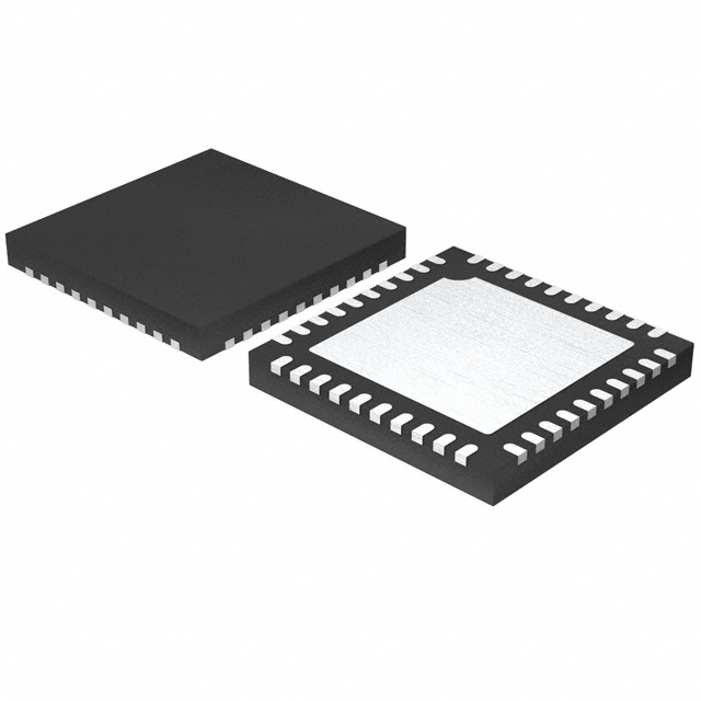
- Part No.:
- CY39C831QN-G-ERE2
- Manufacturer:
- Infineon Technologies
- Category:
- Power Management - Specialized
- Package:
- 40-VFQFN Exposed Pad
- Datasheet:
-
 CY39C831QN-G-ERE2.pdf
- Description:
- IC REG BUCK ENERGY HARVEST 40QFN
- Quantity:
- Payment:

- Shipping:

Inventory:2,269
Please send an inquiry. Send us your inquiry, and we will respond immediately.
Product details
Overview
CY39C831QN-G-ERE2 from Infineon Technologies is a high-speed, low-jitter programmable clock generator IC designed for synchronous digital systems requiring precise timing control. It supports up to four independent output frequencies (up to 700 MHz), features integrated PLL with fractional-N synthesis, operates from a 1.8 V core supply, and uses a 3.3 V I/O supply. It is commonly deployed in FPGA-based communication infrastructure and industrial control systems where deterministic jitter performance (< 0.5 ps RMS) and flexible frequency planning are critical.
For engineers reviewing the CY39C831QN-G-ERE2 datasheet, CY39C831QN-G-ERE2 pinout, CY39C831QN-G-ERE2 application, or CY39C831QN-G-ERE2 equivalent, this device is selected for its configurable output formats (LVDS/LVPECL/HCSL), on-chip EEPROM for nonvolatile configuration storage, and support for spread-spectrum clocking to reduce EMI in dense PCB layouts.
Technical Context
The CY39C831QN-G-ERE2 implements a dual-loop fractional-N PLL architecture with a high-resolution phase interpolator for fine-grained output skew adjustment. Its internal reference input accepts 10–50 MHz crystal or external clock, and each of its four outputs can be independently programmed for frequency, phase offset, and signal format via I²C or SPI interface.
It integrates a 256-byte EEPROM for factory or field-programmable configuration retention across power cycles, and supports dynamic reconfiguration without system reset. The device complies with JEDEC JESD204B/C clocking requirements for high-speed data converters and serial link PHYs.
Key Specifications
| Parameter | Value and Actual Design Meaning |
|---|---|
| Max Output Frequency | 700 MHz - Enables direct clocking of high-speed SerDes lanes and DDR4/5 memory interfaces. |
| RMS Jitter (12 kHz–20 MHz) | 0.45 ps - Meets stringent jitter budget for JESD204B/C ADC/DAC synchronization. |
| Supply Voltages | 1.8 V core / 3.3 V I/O - Supports mixed-voltage SoC/FPGA integration with level-shifted control signaling. |
| Output Formats | LVDS, LVPECL, HCSL - Provides compatibility with multiple receiver standards without external level translation. |
| Configuration Interface | I²C & SPI - Allows in-system programming and runtime frequency switching during operation. |
| EEPROM Size | 256 bytes - Stores full device configuration including PLL settings, output enables, and spread-spectrum parameters. |
Pinout & Package
This device is housed in a 48-pin QFN package (7 mm × 7 mm, 0.5 mm pitch) with exposed thermal pad for enhanced power dissipation in high-frequency operation.
| Pin/Terminal | Circuit Role | Design Meaning |
|---|---|---|
| REFIN | Reference Input | Accepts single-ended or differential crystal or clock source (10–50 MHz); internal biasing enables direct crystal connection. |
| CLKOUT0–CLKOUT3 | Differential Clock Outputs | Four independently configurable outputs supporting LVDS/LVPECL/HCSL; each includes programmable amplitude and common-mode voltage. |
| SCL/SDA | I²C Interface | Two-wire bus for configuration and status readback; supports standard and fast-mode (400 kHz) operation. |
| CS#/SCLK/MOSI/MISO | SPI Interface | Four-pin SPI port for high-speed programming; supports daisy-chain configuration of multiple devices. |
| VDDCORE/VDDIO | Power Supplies | Separate 1.8 V core and 3.3 V I/O rails minimize noise coupling between PLL and digital logic domains. |
| OE# | Output Enable | Active-low global enable controlling all CLKOUT drivers; used for power sequencing and hot-plug synchronization. |
Key Features
| Feature | Design Value |
|---|---|
| Fractional-N PLL with 36-bit N-divider | Enables sub-Hz frequency resolution and eliminates integer boundary spurs in multi-output configurations. |
| Programmable output skew (0–1000 ps step) | Allows precise inter-channel alignment for time-interleaved ADCs or parallel data capture paths. |
| Spread-spectrum modulation (±0.25%, ±0.5%) | Reduces peak EMI by spreading energy across a narrow band, easing EMC compliance without hardware changes. |
| Fail-safe startup mode | Defaults to pre-programmed safe frequency on power-up if EEPROM is corrupted or unconfigured. |
| Thermal shutdown protection | Halts output operation at >125°C junction temperature to prevent damage during sustained high-load conditions. |
Applications
| 5G Radio Unit Timing | FPGA-Based Test Equipment |
|---|---|
Use Scenario: Synchronizing multiple RF transceivers and data converters in massive MIMO active antenna systems. IC Role / Device Role / Timing Role: Primary clock generator providing phase-aligned 122.88 MHz and 245.76 MHz outputs for JESD204B/C links and local oscillator synthesis. Use Value: Sub-0.5 ps jitter ensures <0.1 dB EVM degradation at 28 GHz carrier frequencies under real-world thermal gradients. | Use Scenario: Driving high-speed pattern generators, logic analyzers, and bit-error-rate testers with variable clock rates and skew control. IC Role / Device Role / Timing Role: Reconfigurable master clock source enabling rapid test setup changes without hardware modification. Use Value: On-the-fly frequency switching via SPI allows automated test sequences to adapt clocking per DUT specification without manual intervention. |
| Industrial PLC Backplane Sync | Automotive ADAS Sensor Fusion Hub |
Use Scenario: Distributing synchronized clocks across modular I/O cards and motion controllers in deterministic Ethernet-based automation networks. IC Role / Device Role / Timing Role: Central timing node generating IEEE 1588 PTP grandmaster-compatible clocks and deterministic delay-compensated outputs. Use Value: Programmable output skew compensates for trace-length mismatches across backplane routing, maintaining <1 ns inter-card skew. | Use Scenario: Coordinating radar, camera, and LiDAR sensor sampling in centralized domain controllers for autonomous driving stacks. IC Role / Device Role / Timing Role: Multi-output timing hub delivering phase-locked clocks to heterogeneous sensor interfaces (MIPI CSI-2, AURIX™ T2G, AURIX™ TC3xx). Use Value: Integrated EEPROM retains calibrated skew offsets across vehicle ignition cycles, eliminating boot-time recalibration delays. |
Equivalent & Alternatives
The following parts are listed as comparable options for similar programmable clock generator applications.
| Alternative Part | Technical Difference | Application Difference | Selection Advice |
|---|---|---|---|
| Si5341-B-GM | Higher channel count (12 outputs), wider frequency range (up to 1 GHz), but larger 64-QFN package and higher power consumption (220 mW vs. 145 mW). | Better suited for multi-ASIC SoC platforms requiring >4 outputs; less optimal for space-constrained FPGA mezzanine cards. | Select when needing >4 outputs or tighter absolute accuracy (<±50 ppb) over temperature. |
| LMK04832RHAT | Includes dual cascaded PLLs with jitter cleaning capability (100 fs RMS floor), but lacks on-chip EEPROM and requires external configuration memory. | Preferred for ultra-low-jitter applications like optical transport line cards where jitter accumulation must be minimized across multiple stages. | Select when jitter cleaning is required upstream of high-speed DACs/ADCs and external memory is acceptable. |
Compared with Si5341-B-GM and LMK04832RHAT, the CY39C831QN-G-ERE2 offers the best balance of compact footprint, integrated nonvolatile configuration, and sufficient jitter performance for FPGA-centric designs-without requiring external memory or complex layout for jitter-sensitive analog sections.
Availability
CY39C831QN-G-ERE2 is available at Aetrix Electronics and suitable for 5G radio units, FPGA-based test equipment, industrial PLC backplanes, and automotive ADAS sensor fusion hubs requiring stable component supply and long-term design-in support.
Supply support for CY39C831QN-G-ERE2 includes scheduled delivery planning, volume procurement assistance, BOM continuity management, traceable sourcing, and lifecycle availability coordination for OEM customers, industrial embedded developers, connected-device designers, and electronics production programs.
Manufacturer
Infineon Technologies is a German semiconductor manufacturer specializing in power management, automotive ICs, and industrial control solutions, with global R&D and manufacturing operations.
This part belongs to Infineon's CYPRESS™ Clock generators product line, engineered specifically for high-reliability, programmable timing in FPGA, ASIC, and communications infrastructure applications demanding low jitter and field-configurable flexibility.
FAQ
What is the recommended power supply decoupling scheme for CY39C831QN-G-ERE2?
Use three capacitor values per supply rail: 10 µF tantalum (bulk), 100 nF X7R ceramic (mid-frequency), and 1 nF NP0 ceramic (high-frequency). Place the 1 nF cap within 2 mm of each VDD pin, and connect the thermal pad to a solid 6-layer PCB ground plane using ≥8 thermal vias.
Does CY39C831QN-G-ERE2 support spread-spectrum clocking on individual outputs?
No-spread-spectrum modulation applies globally to all enabled outputs simultaneously. The feature is controlled via register bit SSM_EN and modulates the VCO frequency across the entire output set; per-output modulation is not supported in this generation.
Can the device retain configuration after power loss without external memory?
Yes-the integrated 256-byte EEPROM stores full configuration, including PLL settings, output enables, format selections, and spread-spectrum parameters. Configuration persists across power cycles and requires no external memory or host initialization.
Is there a hardware reset pin, and what is its behavior?
Yes-pin RST# is an active-low asynchronous reset that forces the device into default state: all outputs disabled, PLL bypassed, and internal registers cleared. It does not erase EEPROM contents; configuration reloads automatically upon release if EEPROM is valid.
CY39C831QN-G-ERE2 Specifications
- Product attributes
- Attribute value
- Manufacturer:
- Infineon Technologies
- Series:
- -
- Package/Case:
- 40-VFQFN Exposed Pad
- Packaging:
- Cut Tape (CT)
- Product Status:
- Obsolete
- Applications:
- Energy Harvesting
- Current - Supply:
- 32µA
- Voltage - Supply:
- 3V ~ 5V
- Operating Temperature:
- -40°C ~ 85°C
- Grade:
- -
- Qualification:
- -
- Mounting Type:
- Surface Mount
- Supplier Device Package:
- 40-QFN (6x6)
CY39C831QN-G-ERE2 FAQ
1.How can I place an order for CY39C831QN-G-ERE2 through Aetrix?
Please submit a Request for Quotation (RFQ) for CY39C831QN-G-ERE2 on Aetrix. Our sales agent will provide a competitive quotation and guide you through the order confirmation once you accept the terms.
2.Are the price and stock information for CY39C831QN-G-ERE2 reliable?
The price and inventory of CY39C831QN-G-ERE2 are updated periodically and may fluctuate due to market conditions. Stock and pricing data are typically refreshed every 24 hours. Quotation validity for CY39C831QN-G-ERE2 is usually 5 days.
3.What payment methods are accepted for CY39C831QN-G-ERE2?
We accept Wire Transfer, PayPal, Credit Card, Western Union, MoneyGram, and Escrow for CY39C831QN-G-ERE2 transactions.
Note: Certain payment methods may incur a processing fee.
4.How is shipping managed for CY39C831QN-G-ERE2?
CY39C831QN-G-ERE2 orders can be shipped via leading logistics carriers, including DHL, UPS, FedEx, TNT, or Registered Mail.
Once your CY39C831QN-G-ERE2 order is processed, you will receive an email with the shipment details and tracking number.
Note: Tracking information may take up to 24 hours to appear. Express delivery typically takes 3–5 business days.
5.How can I obtain technical support or documentation for CY39C831QN-G-ERE2?
For technical support, including CY39C831QN-G-ERE2 datasheets, pinout diagrams, or application guidance, please contact our engineering support team. They can provide detailed documentation and assistance for your CY39C831QN-G-ERE2 requirements.
6.How does Aetrix verify that CY39C831QN-G-ERE2 is sourced from the original manufacturer or authorized distributors?
All CY39C831QN-G-ERE2 products on Aetrix are procured from qualified distributors and authorized channels. Our dedicated quality assurance team conducts strict verification, including traceability checks and, if necessary, third-party testing. This ensures that CY39C831QN-G-ERE2 meets industry standards.
7.What is the process for return or replacement of CY39C831QN-G-ERE2?
All CY39C831QN-G-ERE2 units undergo pre-shipment inspection (PSI). If there is an issue with CY39C831QN-G-ERE2, returns or replacements are accepted under the following conditions:
1.Quantity discrepancies, incorrect items, or visible external defects (such as breakage or corrosion), acknowledged by Aetrix.
2.The issue is reported within 90 days of delivery.
3.The CY39C831QN-G-ERE2 part is unused and in its original packaging.
Return procedure for CY39C831QN-G-ERE2:
1.Submit a request within 90 days.
2.Obtain a Return Material Authorization (RMA) from Aetrix.
CY39C831QN-G-ERE2 Tags

-
TPS2511DGNR
Texas Instruments

-
UTC2000/MG
Microchip Technology

-
TUSB320HAIRWBR
Texas Instruments

-
TPS61252DSGR
Texas Instruments

-
PI5USB30216CXUAEX
Diodes Incorporated

-
SN6501DBVR
Texas Instruments

-
CYPD3177-24LQXQT
Infineon Technologies
-
SN6501QDBVRQ1
Texas Instruments

-
STUSB1600AQTR
STMicroelectronics

-
SN6505BDBVR
Texas Instruments
-
SN6501DBVT
Texas Instruments

-
TPS65150PWPR
Texas Instruments
Tech Hub

18650 battery guide covering lithium-ion cell basics, 3.6V/3.7V voltage, 4.2V charging, mAh and Wh capacity, protected cells, chargers, BMS, series-parallel packs, holders, welding and sourcing checks.…

Hall effect sensor guide covering working principle, linear and digital sensors, Arduino circuits, current sensing, speed detection, automotive applications, A3144 examples, signal filtering and datash…

Product Change Notification guide for electronic components, covering PCN meaning, PCN vs PDN/EOL, common change types, risk levels, form-fit-function review, engineering validation, BOM control, LTB/L…

A practical guide to blend door actuators, covering HVAC function, symptoms, location, AC and heater issues, reset and calibration, replacement cost, electrical diagnosis, compatibility checks, and rep…

Engineering guide to Raspberry Pi alternatives, covering chip-level differences, Orange Pi, ROCK, Jetson, Banana Pi, NanoPi, Compute Module, Pico, GPIO, camera, HAT compatibility, and replacement risks…

Engineering guide to dynamic load response testing for high-current buck converters, covering load step setup, slew rate, Vcore undershoot, overshoot, recovery time, probe location, output capacitors a…

Engineering guide to output capacitor selection for ASIC Vcore rails, covering bulk capacitors, polymer capacitors, MLCC decoupling, DC bias, ESR, ESL, placement, transient response and substitution ri…

Engineering guide to high-current ASIC Vcore rails, covering 12-phase buck architecture, PMBus control, dynamic load testing, output capacitor networks, smart power stage selection, thermal design and …

Voltage regulator guide covering linear, LDO, 7805, Zener, adjustable, buck, VRM and alternator regulators, with design checks, testing methods, troubleshooting and datasheet-based selection.

Amplifier guide covering voltage, current and power amplification, gain, feedback, amplifier classes, audio and RF applications, op-amp circuits, transimpedance amplifiers, datasheet selection and trou…


