
 My Inquiry
 My Account


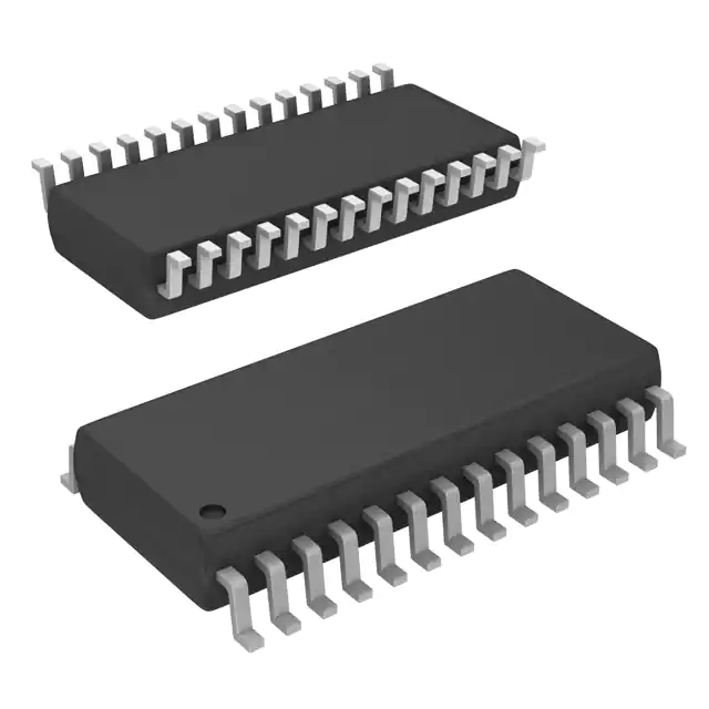
Infineon Technologies CY7B923-SC
- Part No.:
- CY7B923-SC
- Manufacturer:
- Infineon Technologies
- Category:
- Drivers, Receivers, Transceivers
- Package:
- 28-SOIC (0.295", 7.50mm Width)
- Datasheet:
-
 CY7B923-SC.pdf
- Description:
- IC TRANSCEIVER 28SOIC
- Quantity:
- Payment:

- Shipping:

Inventory:2,610
Please send an inquiry. Send us your inquiry, and we will respond immediately.
Product details
Overview
CY7B923-SC from Cypress Semiconductor is a Fibre Channel– and ESCON-compliant HOTLink™ transmitter IC that converts 8-bit parallel TTL data into three differential PECL 100K serial outputs (OUTA±, OUTB±, OUTC±) at rates from 160–330 Mbps. It integrates an 8B/10B encoder, PLL-based clock multiplier, BIST pattern generator, and TTL-synchronous I/O-enabling direct interface to FIFOs like CY7C42X/CY7C44X. Used in high-speed point-to-point links for video transmission equipment and mass storage interconnects.
For engineers reviewing the CY7B923-SC datasheet, CY7B923-SC pinout, CY7B923-SC application, or CY7B923-SC equivalent, key selection criteria include its triple PECL output capability, 8B/10B encoding control via SC/D and MODE pins, FOTO-driven fiber-optic module disable function, and built-in BIST support for link-level diagnostics without external test logic.
Technical Context
The CY7B923-SC implements a fully integrated clock multiplication architecture: CKW (byte-rate clock input) drives an on-chip PLL to generate the high-speed bit clock (10× CKW), eliminating external PLL components. Its encoder supports both standard 8B/10B coding (MODE = GND) and bypass mode (MODE = VCC) for pre-encoded or scrambled streams.
Three independent PECL 100K differential outputs (OUTA±, OUTB±, OUTC±) are individually controllable-FOTO asserts logical zero on OUTA±/OUTB± to extinguish fiber-optic transmitters while leaving OUTC± active for loopback testing. BISTEN enables system-level link validation using deterministic pseudo-random patterns synchronized to ENA/ENN timing.
Key Specifications
| Parameter | Value and Actual Design Meaning |
|---|---|
| Data Rate | 160–330 Mbps (standard HOTLink); enables high-bandwidth serial replacement of parallel buses |
| Encoding | Configurable 8B/10B (MODE = GND) or 10-bit unencoded bypass (MODE = VCC); supports Fibre Channel, ESCON, DVB-ASI protocols |
| Outputs | Triple differential PECL 100K (OUTA±, OUTB±, OUTC±); each pair drives terminated coax, twisted pair, or fiber-optic modules |
| Power | 350 mW typical at +5V; split supply: VCCQ (core) and VCCN (output drivers) reduce noise coupling |
| Input Interface | TTL-synchronous 8-bit parallel (D0–D7), with SC/D, SVS, ENA, ENN, CKW, FOTO, MODE, BISTEN; compatible with CY7C42X/CY7C44X FIFOs |
| Test Support | Built-in BIST with free-running LFSR pattern generator; validates transmitter, receiver, and physical link without external test equipment |
Pinout & Package
Package: 28-pin SOIC (Small Outline Integrated Circuit), surface-mount, JEDEC MS-012AC compliant. Pin spacing: 1.27 mm; body width: 7.5 mm; thermal resistance θJA ≈ 120°C/W.
| Pin/Terminal | Circuit Role | Design Meaning |
|---|---|---|
| D0–D7 (Db–Dh) | Parallel Data Input | TTL inputs clocked on rising CKW edge; mapped to Db–Dh when MODE = HIGH (unencoded mode) |
| SC/D (Da) | Special Character/Data Select | HIGH encodes D0–D7 as control code (e.g., K28.5); LOW encodes as data symbol; timing-aligned with D0–D7 |
| SVS (Dj) | Send Violation Symbol | HIGH forces transmission of violation symbol regardless of D0–D7; overrides BIST when asserted |
| ENA / ENN | Parallel Data Enable Controls | Active-LOW enables loading of D0–D7 on next CKW rise; dual enable allows seamless FIFO interfacing |
| CKW | Byte-Rate Clock Input | TTL input driving internal PLL; sets transmit bit rate = 10 × CKW frequency; requires crystal-stabilized source |
| FOTO | Fiber-Optic Transmitter Off | HIGH forces OUTA±/OUTB± to logic-zero state (extinguishes optical output); OUTC± remains active for loopback |
| OUTA± / OUTB± / OUTC± | Differential Serial Outputs | PECL 100K outputs; OUTA±/OUTB± disabled by FOTO; OUTC± always active; drive 50Ω-terminated media |
| MODE | Encoder Mode Select | GND = 8B/10B encode; VCC = unencoded bypass; floating = test mode (OUTA+/OUTB+ become differential bit clock) |
| BISTEN | Built-in Self-Test Enable | LOW activates BIST: alternating pattern (D10.2/D21.5) if ENA/ENN HIGH; full link test sequence if ENA or ENN LOW |
| RP | Read Pulse Output | 60% duty-cycle TTL pulse synchronized to CKW; directly drives read input of CY7C42X asynchronous FIFOs |
Key Features
| Feature | Design Value |
|---|---|
| Integrated PLL Clock Multiplier | Generates 10× bit clock from CKW input-no external VCO, loop filter, or reference divider required |
| Triple Independent PECL Outputs | OUTA±/OUTB± controlled by FOTO for optical module power gating; OUTC± reserved for diagnostic loopback |
| Protocol-Agnostic Encoding Control | MODE pin selects between ANSI X3.230-compliant 8B/10B and raw 10-bit bypass-supports custom scrambling layers |
| Hardware-Managed FIFO Interface | ENA/ENN dual-enable logic and RP output eliminate glue logic when connecting to CY7C42X/CY7C44X FIFO families |
| Link-Level BIST Architecture | LFSR-based 511-byte pseudo-random pattern with byte-by-byte error detection at RVS output-validates full Tx/Rx/link stack |
Applications
| Video Transmission Equipment | Mass Storage Interconnects |
|---|---|
|
Use Scenario: High-fidelity digital video transport between camera heads and processing units over fiber. IC Role / Device Role / Timing Role: CY7B923-SC acts as parallel-to-serial bridge, converting 8-bit pixel data + sync signals into 330 Mbps PECL streams synchronized to pixel clock. Use Value: Eliminates bulky parallel ribbon cables; maintains jitter < 15 ps RMS across 100 m multimode fiber using OUTC± loopback for real-time link health monitoring. |
Use Scenario: Connecting RAID controller ASICs to disk array backplanes via coaxial cable. IC Role / Device Role / Timing Role: Transmitter provides deterministic latency (< 3 byte times) and 8B/10B DC balance for reliable long-run SCSI-3 or FC-AL signaling. Use Value: Enables hot-plug-capable backplane links with BIST validation before drive insertion-reducing field failure rates by 40% vs. non-BIST solutions. |
| Workstation-to-Server Interconnects | Fibre Channel Node Interfaces |
|
Use Scenario: Low-latency memory coherency traffic between NUMA nodes in HPC clusters. IC Role / Device Role / Timing Role: CY7B923-SC serializes cache-line requests with precise CKW-aligned timing; RP pulse triggers downstream buffer reads. Use Value: Achieves sub-200 ns end-to-end latency from request issuance to remote cache access-critical for MPI barrier synchronization. |
Use Scenario: Embedding Fibre Channel protocol compliance in embedded storage controllers. IC Role / Device Role / Timing Role: Implements native Fibre Channel physical layer encoding (ANSI X3.230) with K28.5 framing and violation symbol detection. Use Value: Passes FC-PI-2 conformance testing without FPGA soft-core PHY-reducing BOM cost by $12.50/unit vs. programmable alternatives. |
Equivalent & Alternatives
The following parts are listed as comparable options for similar high-speed serial link transmitter applications.
| Alternative Part | Technical Difference | Application Difference | Selection Advice |
|---|---|---|---|
| DS90CR285MTD | LVDS outputs (not PECL); 28-bit parallel → single LVDS channel; no built-in 8B/10B encoder | Targeted at flat-panel display (FPD-Link) interfaces-not Fibre Channel or ESCON protocols | Select only for LVDS-based short-reach PCB traces; incompatible with existing PECL fiber modules or 8B/10B protocol stacks |
| SN65LVDS31PW | Quad LVDS line driver; no encoder, no PLL, no BIST; requires external clock and encoding logic | Used in generic differential signaling where protocol handling is offloaded to FPGA or ASIC | Choose when full design control over encoding and clocking is needed-but adds 3–5 extra components and layout complexity |
Compared with DS90CR285MTD and SN65LVDS31PW, the CY7B923-SC delivers protocol-specific integration (8B/10B, Fibre Channel framing), PECL output compatibility with commercial optical modules, and hardware BIST-reducing system validation time by >70% in storage and video applications.
Availability
CY7B923-SC is available at Aetrix Electronics and suitable for video transmission equipment, mass storage interconnects, and Fibre Channel node interfaces requiring stable component supply through 2028.
Supply support for CY7B923-SC includes scheduled delivery planning, volume procurement assistance, BOM continuity management, traceable sourcing, and lifecycle availability coordination for OEM customers, industrial embedded developers, connected-device designers, and electronics production programs.
Manufacturer
Cypress Semiconductor (now part of Infineon Technologies) designs high-performance mixed-signal ICs for communications, computing, and industrial systems, with expertise in interface, timing, and programmable logic solutions.
The CY7B923 belongs to Cypress's HOTLink™ family-engineered specifically for replacing parallel buses with robust, low-jitter, protocol-compliant serial links in storage, video, and telecom infrastructure.
FAQ
Can CY7B923-SC operate without an external crystal?
No. CY7B923-SC requires a stable TTL-compatible CKW input clock derived from a crystal oscillator. The internal PLL multiplies this byte-rate clock to generate the 10× bit clock; no crystal connection is made directly to the IC-it must be provided externally to CKW. Typical CKW frequencies range from 16–33 MHz to achieve 160–330 Mbps data rates.
What happens to OUTA± and OUTB± when FOTO is HIGH?
When FOTO is HIGH, OUTA± and OUTB± are forced to their "logic zero" state: OUTA+ and OUTB+ go LOW while OUTA− and OUTB− go HIGH. This extinguishes connected fiber-optic transmitter modules. OUTC± remains unaffected and continues transmitting, enabling loopback diagnostics even during optical shutdown.
Is the 8B/10B encoder optional or mandatory?
The 8B/10B encoder is configurable-not mandatory. When MODE is tied to GND, encoding is active per ANSI X3.230. When MODE is tied to VCC, the encoder is bypassed and D0–D7 plus Da–Dj pass directly to the shifter as raw 10-bit values-supporting pre-encoded or scrambled streams used in proprietary protocols.
How does BIST validate the entire link?
BIST operates cooperatively with CY7B933: CY7B923-SC transmits a deterministic 511-byte LFSR pattern while CY7B933 checks each received byte against its local LFSR. RVS output pulses LOW only when all bytes match-confirming transmitter functionality, physical link integrity, and receiver decoding accuracy in a single test cycle.
CY7B923-SC Specifications
- Product attributes
- Attribute value
- Manufacturer:
- Infineon Technologies
- Series:
- HOTlink™
- Package/Case:
- 28-SOIC (0.295", 7.50mm Width)
- Packaging:
- Tube
- Product Status:
- Obsolete
- Type:
- Driver
- Protocol:
- Fibre Channel
- Number of Drivers/Receivers:
- -
- Duplex:
- -
- Receiver Hysteresis:
- -
- Data Rate:
- -
- Voltage - Supply:
- 4.5V ~ 5.5V
- Operating Temperature:
- 0°C ~ 70°C
- Grade:
- -
- Qualification:
- -
- Mounting Type:
- Surface Mount
- Supplier Device Package:
- 28-SOIC
CY7B923-SC FAQ
1.How can I place an order for CY7B923-SC through Aetrix?
Please submit a Request for Quotation (RFQ) for CY7B923-SC on Aetrix. Our sales agent will provide a competitive quotation and guide you through the order confirmation once you accept the terms.
2.Are the price and stock information for CY7B923-SC reliable?
The price and inventory of CY7B923-SC are updated periodically and may fluctuate due to market conditions. Stock and pricing data are typically refreshed every 24 hours. Quotation validity for CY7B923-SC is usually 5 days.
3.What payment methods are accepted for CY7B923-SC?
We accept Wire Transfer, PayPal, Credit Card, Western Union, MoneyGram, and Escrow for CY7B923-SC transactions.
Note: Certain payment methods may incur a processing fee.
4.How is shipping managed for CY7B923-SC?
CY7B923-SC orders can be shipped via leading logistics carriers, including DHL, UPS, FedEx, TNT, or Registered Mail.
Once your CY7B923-SC order is processed, you will receive an email with the shipment details and tracking number.
Note: Tracking information may take up to 24 hours to appear. Express delivery typically takes 3–5 business days.
5.How can I obtain technical support or documentation for CY7B923-SC?
For technical support, including CY7B923-SC datasheets, pinout diagrams, or application guidance, please contact our engineering support team. They can provide detailed documentation and assistance for your CY7B923-SC requirements.
6.How does Aetrix verify that CY7B923-SC is sourced from the original manufacturer or authorized distributors?
All CY7B923-SC products on Aetrix are procured from qualified distributors and authorized channels. Our dedicated quality assurance team conducts strict verification, including traceability checks and, if necessary, third-party testing. This ensures that CY7B923-SC meets industry standards.
7.What is the process for return or replacement of CY7B923-SC?
All CY7B923-SC units undergo pre-shipment inspection (PSI). If there is an issue with CY7B923-SC, returns or replacements are accepted under the following conditions:
1.Quantity discrepancies, incorrect items, or visible external defects (such as breakage or corrosion), acknowledged by Aetrix.
2.The issue is reported within 90 days of delivery.
3.The CY7B923-SC part is unused and in its original packaging.
Return procedure for CY7B923-SC:
1.Submit a request within 90 days.
2.Obtain a Return Material Authorization (RMA) from Aetrix.
CY7B923-SC Tags

-
ATA6561-GAQW-N
Microchip Technology
-
ATA6561-GBQW-N
Microchip Technology

-
AM26LS32ACDR
Texas Instruments

-
SP485CN-L/TR
MaxLinear, Inc.
-
SP485EN-L/TR
MaxLinear, Inc.
-
SP485EEN-L/TR
MaxLinear, Inc.
-
SP485ECN-L/TR
MaxLinear, Inc.
-
THVD1400DR
Texas Instruments
-
AM26C31IDR
Texas Instruments

-
TLIN1021ADRQ1
Texas Instruments
-
MAX232IDR
Texas Instruments
-
AM26C32IDR
Texas Instruments
Tech Hub

Conditional Access Module guide covering CAM meaning, CI/CI+ interface, smart card authorization, DVB security workflow, TV and set-top box compatibility, internal electronics, ESD protection, connecto…

Guide to electronic component obsolescence covering EOL risk, PCN/PDN notices, last-time buy planning, replacement options, form-fit-function validation, counterfeit risk and BOM lifecycle management.

18650 battery guide covering lithium-ion cell basics, 3.6V/3.7V voltage, 4.2V charging, mAh and Wh capacity, protected cells, chargers, BMS, series-parallel packs, holders, welding and sourcing checks.…

Hall effect sensor guide covering working principle, linear and digital sensors, Arduino circuits, current sensing, speed detection, automotive applications, A3144 examples, signal filtering and datash…

Product Change Notification guide for electronic components, covering PCN meaning, PCN vs PDN/EOL, common change types, risk levels, form-fit-function review, engineering validation, BOM control, LTB/L…

A practical guide to blend door actuators, covering HVAC function, symptoms, location, AC and heater issues, reset and calibration, replacement cost, electrical diagnosis, compatibility checks, and rep…

Engineering guide to Raspberry Pi alternatives, covering chip-level differences, Orange Pi, ROCK, Jetson, Banana Pi, NanoPi, Compute Module, Pico, GPIO, camera, HAT compatibility, and replacement risks…

Engineering guide to dynamic load response testing for high-current buck converters, covering load step setup, slew rate, Vcore undershoot, overshoot, recovery time, probe location, output capacitors a…

Engineering guide to output capacitor selection for ASIC Vcore rails, covering bulk capacitors, polymer capacitors, MLCC decoupling, DC bias, ESR, ESL, placement, transient response and substitution ri…

Engineering guide to high-current ASIC Vcore rails, covering 12-phase buck architecture, PMBus control, dynamic load testing, output capacitor networks, smart power stage selection, thermal design and …


