
 My Inquiry
 My Account


Cypress Semiconductor Corp CY7C0241E-15AXC
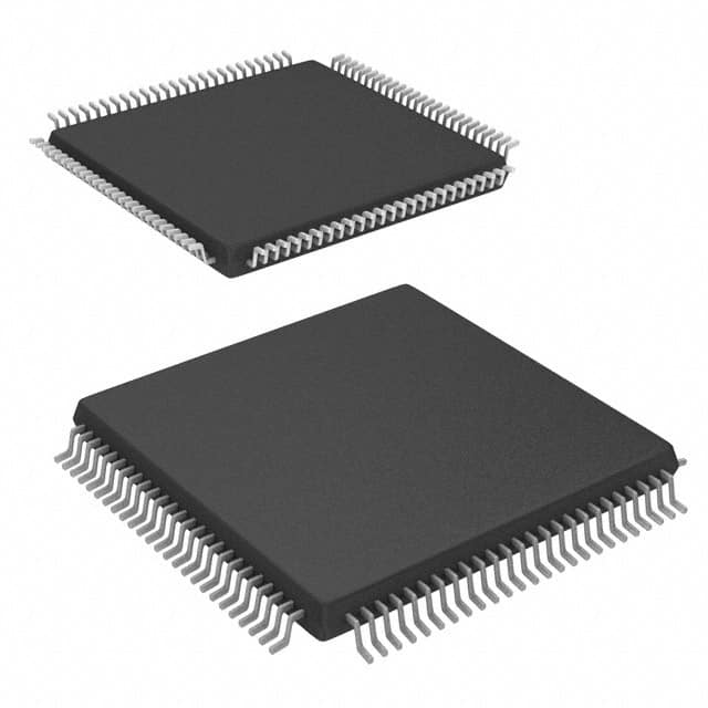
- Part No.:
- CY7C0241E-15AXC
- Manufacturer:
- Cypress Semiconductor Corp
- Category:
- Memory
- Package:
- 100-LQFP
- Datasheet:
-
 CY7C0241E-15AXC.pdf
- Description:
- IC SRAM 72KBIT PARALLEL 100TQFP
- Quantity:
- Payment:

- Shipping:

Inventory:3,866
Please send an inquiry. Send us your inquiry, and we will respond immediately.
Product details
Overview
CY7C0241E-15AXC from Cypress Semiconductor is a 4K × 18-bit true dual-port static RAM with independent left/right ports, 15 ns access time, on-chip semaphore logic, and BUSY/INT flags for interprocessor coordination-used in real-time video buffering and multiprocessor shared-memory systems.
For engineers reviewing the CY7C0241E-15AXC datasheet, CY7C0241E-15AXC pinout, CY7C0241E-15AXC application, or CY7C0241E-15AXC equivalent, key selection criteria include asynchronous dual-port arbitration timing, M/S-configurable master/slave expansion, 18-bit data width support, and Pb-free 100-pin TQFP packaging for high-density embedded designs.
Technical Context
This device implements fully asynchronous dual-port operation with separate CE/R/W/OE controls per port, enabling concurrent read/write access to any memory location. Its on-chip arbitration resolves contention via deterministic BUSY assertion (tBLA/tBLC) and supports software handshaking through eight dedicated semaphore latches accessed via SEM pin.
The interrupt mechanism uses upper two memory addresses (0xFFE/0xFFF) as mailboxes: write to opposite port's mailbox triggers INT flag; reading resets it. BUSY signal behavior changes with M/S pin state-output in master mode, input in slave mode-enabling seamless 36-bit expansion without external logic.
Key Specifications
| Parameter | Value and Actual Design Meaning |
|---|---|
| Memory Organization | 4K × 18 bits (72 Kbit total), supporting independent 18-bit data paths per port |
| Access Time | 15 ns maximum-guarantees deterministic latency for real-time interprocessor communication |
| Operating Current | 180 mA typical-enables low-power operation in battery-backed or thermally constrained systems |
| Standby Current | 0.05 mA typical (ISB3)-supports automatic power-down per port via CE control |
| Supply Voltage | 3.3 V ±0.3 V-compatible with modern low-voltage digital logic families |
| Package | 100-pin Pb-free TQFP (14 mm × 14 mm)-meets RoHS requirements and enables high-density PCB layout |
| Arbitration Logic | On-chip hardware arbitration with BUSY flag and tPS setup window-eliminates need for external bus controllers |
Pinout & Package
Package: 100-pin thin quad flatpack (TQFP), Pb-free, 14 mm × 14 mm body, 0.5 mm pitch.
| Pin/Terminal | Circuit Role | Design Meaning |
|---|---|---|
| CEL / CER | Chip Enable (Left/Right) | Independent port activation; drives automatic power-down when deasserted |
| R/WL / R/WR | Read/Write Control (Left/Right) | Edge-triggered write enable; rising edge initiates write with tSD setup requirement |
| OEL / OER | Output Enable (Left/Right) | Controls tri-state output drivers; allows independent read gating per port |
| SEML / SEMR | Semaphore Enable (Left/Right) | Chip-select for 8 semaphore latches; overrides CE during semaphore access |
| INTL / INTR | Interrupt Flag (Left/Right) | Open-drain output signaling mailbox write from opposite port; reset by local read |
| BUSYL / BUSYR | Busy Flag (Left/Right) | Indicates arbitration conflict; output in master mode, input in slave mode |
| M/S | Master/Slave Select | Configures BUSY pin direction and enables 36-bit expansion without external logic |
| I/O0L–I/O17L / I/O0R–I/O17R | Data Bus (Left/Right) | 18-bit bidirectional data path per port; UBL/LBL allow byte-selectable writes |
Key Features
| Feature | Design Value |
|---|---|
| True dual-port memory cells | Enables simultaneous reads of identical addresses-critical for coherent status mirroring in lockstep processors |
| On-chip semaphore logic (8 latches) | Eliminates need for external mutex hardware; supports atomic resource allocation across ports |
| Configurable master/slave mode (M/S pin) | Permits 36-bit wide memory expansion using multiple devices without discrete glue logic |
| Dual mailbox interrupt system | Uses FFE/FFF addresses for deterministic port-to-port messaging-no polling required |
| Separate upper/lower byte control (UBL/LBL) | Allows partial-word writes without read-modify-write cycles-reduces bus traffic in mixed-data-width systems |
Applications
| Real-Time Video Frame Buffering | Multiprocessor Shared Memory |
|---|---|
Use Scenario: Dual-port SRAM buffers live video frames between image sensor interface and display controller. IC Role / Device Role / Timing Role: Left port accepts pixel data at sensor clock rate; right port supplies display engine at scan-out rate-both accessing same frame buffer concurrently. Use Value: Eliminates frame tearing and reduces latency by enabling zero-copy frame handoff without CPU intervention. | Use Scenario: Two ARM Cortex-A cores share configuration tables and status registers in an industrial PLC. IC Role / Device Role / Timing Role: Acts as coherent shared memory with hardware arbitration-prevents race conditions during register updates. Use Value: Reduces software overhead by replacing spinlocks with hardware semaphore latches and BUSY-driven backoff. |
| Communications Protocol Stack Buffering | DSP Co-Processor Data Exchange |
Use Scenario: Ethernet MAC and TCP/IP stack processor exchange packet descriptors and payload fragments. IC Role / Device Role / Timing Role: Left port handles descriptor ring management; right port manages payload DMA transfers-coordinated via INT/SEM flags. Use Value: Enables full-duplex packet processing with deterministic interrupt latency (<15 ns access ensures timely descriptor updates). | Use Scenario: Main MCU offloads FFT computation to dedicated DSP; results are written to shared memory region. IC Role / Device Role / Timing Role: Provides non-blocking data exchange channel with mailbox-based completion signaling between heterogeneous processors. Use Value: Avoids bus contention delays-DSP writes result, asserts INTR; MCU reads result and clears flag within same 15 ns cycle budget. |
Equivalent & Alternatives
The following parts are listed as comparable options for similar dual-port SRAM applications.
| Alternative Part | Technical Difference | Application Difference | Selection Advice |
|---|---|---|---|
| IDT70V25L15PF | 4K × 16 organization, 15 ns access, 100-pin TQFP-but lacks integrated semaphores and INT mailboxes | Requires external logic for resource arbitration and inter-port signaling | Select when only basic dual-port functionality is needed and external arbitration is acceptable |
| ISSI IS61WV25616BLL-15TLI | 256K × 16 async SRAM, single-port only, 15 ns-no dual-port capability or BUSY/SEM logic | Cannot support simultaneous access or hardware-coordinated multi-processor sharing | Use only in legacy single-CPU systems where dual-port features are unnecessary |
Compared with IDT70V25L15PF and IS61WV25616BLL-15TLI, CY7C0241E-15AXC delivers integrated arbitration, mailbox interrupts, and semaphores-reducing BOM count and firmware complexity in tightly coupled multiprocessor designs requiring deterministic shared-memory access.
Availability
CY7C0241E-15AXC is available at Aetrix Electronics and suitable for real-time video buffering, multiprocessor shared memory, and communications protocol stack buffering requiring stable component supply and long-term lifecycle support.
Supply support for CY7C0241E-15AXC includes scheduled delivery planning, volume procurement assistance, BOM continuity management, traceable sourcing, and lifecycle availability coordination for OEM customers, industrial embedded developers, connected-device designers, and electronics production programs.
Manufacturer
Cypress Semiconductor (now part of Infineon Technologies) designs high-performance memory and programmable solutions for embedded systems, emphasizing reliability and integration.
CY7C0241E belongs to Cypress's dual-port SRAM product line, engineered specifically for deterministic interprocessor communication in real-time embedded systems with strict timing and coherency requirements.
FAQ
What is the function of the M/S pin on CY7C0241E-15AXC?
The M/S pin configures the device as master (M/S = HIGH) or slave (M/S = LOW). In master mode, BUSY pins act as outputs signaling arbitration outcomes; in slave mode, they become inputs accepting BUSY from a master. This enables 36-bit memory expansion without external logic or discrete bus controllers.
How does semaphore operation work without conflicting with main memory access?
Semaphores reside in eight dedicated latches separate from the 4K × 18 memory array. Access requires asserting SEM (not CE), with A0–A2 selecting the latch. During SEM access, CE must remain HIGH, and only I/O0 is used for write data-ensuring no interference with normal memory reads/writes or data integrity.
Can both ports perform simultaneous reads to the same address?
Yes-true dual-port architecture allows concurrent reads to identical addresses without contention or BUSY assertion. Each port has independent sense amplifiers and output drivers, enabling coherent status mirroring and lockstep monitoring in safety-critical applications.
What happens if both ports attempt to write to the same location simultaneously?
On-chip arbitration asserts BUSY on the losing port after tBLA (address match) or tBLC (CE assertion). The winning port gains immediate access; the losing port must wait until BUSY deasserts before retrying. If tPS setup window is violated, arbitration outcome becomes unpredictable-designs must meet tPS timing to ensure determinism.
CY7C0241E-15AXC Specifications
- Product attributes
- Attribute value
- Manufacturer:
- Cypress Semiconductor Corp
- Series:
- -
- Package/Case:
- 100-LQFP
- Packaging:
- Bulk
- Product Status:
- Active
- Programmable:
- Not Verified
- Memory Type:
- Volatile
- Memory Format:
- SRAM
- Technology:
- SRAM - Dual Port, Asynchronous
- Memory Size:
- 72Kbit
- Memory Organization:
- 4K x 18
- Memory Interface:
- Parallel
- Clock Frequency:
- -
- Write Cycle Time - Word, Page:
- 15ns
- Access Time:
- 15 ns
- Voltage - Supply:
- 4.5V ~ 5.5V
- Operating Temperature:
- 0°C ~ 70°C (TA)
- Grade:
- -
- Qualification:
- -
- Mounting Type:
- Surface Mount
- Supplier Device Package:
- 100-TQFP (14x14)
CY7C0241E-15AXC FAQ
1.How can I place an order for CY7C0241E-15AXC through Aetrix?
Please submit a Request for Quotation (RFQ) for CY7C0241E-15AXC on Aetrix. Our sales agent will provide a competitive quotation and guide you through the order confirmation once you accept the terms.
2.Are the price and stock information for CY7C0241E-15AXC reliable?
The price and inventory of CY7C0241E-15AXC are updated periodically and may fluctuate due to market conditions. Stock and pricing data are typically refreshed every 24 hours. Quotation validity for CY7C0241E-15AXC is usually 5 days.
3.What payment methods are accepted for CY7C0241E-15AXC?
We accept Wire Transfer, PayPal, Credit Card, Western Union, MoneyGram, and Escrow for CY7C0241E-15AXC transactions.
Note: Certain payment methods may incur a processing fee.
4.How is shipping managed for CY7C0241E-15AXC?
CY7C0241E-15AXC orders can be shipped via leading logistics carriers, including DHL, UPS, FedEx, TNT, or Registered Mail.
Once your CY7C0241E-15AXC order is processed, you will receive an email with the shipment details and tracking number.
Note: Tracking information may take up to 24 hours to appear. Express delivery typically takes 3–5 business days.
5.How can I obtain technical support or documentation for CY7C0241E-15AXC?
For technical support, including CY7C0241E-15AXC datasheets, pinout diagrams, or application guidance, please contact our engineering support team. They can provide detailed documentation and assistance for your CY7C0241E-15AXC requirements.
6.How does Aetrix verify that CY7C0241E-15AXC is sourced from the original manufacturer or authorized distributors?
All CY7C0241E-15AXC products on Aetrix are procured from qualified distributors and authorized channels. Our dedicated quality assurance team conducts strict verification, including traceability checks and, if necessary, third-party testing. This ensures that CY7C0241E-15AXC meets industry standards.
7.What is the process for return or replacement of CY7C0241E-15AXC?
All CY7C0241E-15AXC units undergo pre-shipment inspection (PSI). If there is an issue with CY7C0241E-15AXC, returns or replacements are accepted under the following conditions:
1.Quantity discrepancies, incorrect items, or visible external defects (such as breakage or corrosion), acknowledged by Aetrix.
2.The issue is reported within 90 days of delivery.
3.The CY7C0241E-15AXC part is unused and in its original packaging.
Return procedure for CY7C0241E-15AXC:
1.Submit a request within 90 days.
2.Obtain a Return Material Authorization (RMA) from Aetrix.
CY7C0241E-15AXC Tags

-
M24C02-WMN6TP
STMicroelectronics

-
AT24C02C-XHM-T
Microchip Technology

-
AT21CS01-STUM10-T
Microchip Technology

-
AT24C02C-SSHM-T
Microchip Technology

-
24LC01BT-I/OT
Microchip Technology

-
M24C02-FMC6TG
STMicroelectronics
-
AT24CS02-SSHM-T
Microchip Technology

-
93LC46BT-I/OT
Microchip Technology
-
AT24C04C-SSHM-T
Microchip Technology

-
24LC01BT-I/SN
Microchip Technology
-
24AA02UIDT-I/OT
Microchip Technology

-
AT24C08C-STUM-T
Microchip Technology
Tech Hub

LDO regulator guide covering low dropout voltage, power dissipation, thermal design, PSRR, output noise, capacitor stability, adjustable LDO circuits, LDO vs buck converter and datasheet selection chec…

Conditional Access Module guide covering CAM meaning, CI/CI+ interface, smart card authorization, DVB security workflow, TV and set-top box compatibility, internal electronics, ESD protection, connecto…

Guide to electronic component obsolescence covering EOL risk, PCN/PDN notices, last-time buy planning, replacement options, form-fit-function validation, counterfeit risk and BOM lifecycle management.

18650 battery guide covering lithium-ion cell basics, 3.6V/3.7V voltage, 4.2V charging, mAh and Wh capacity, protected cells, chargers, BMS, series-parallel packs, holders, welding and sourcing checks.…

Hall effect sensor guide covering working principle, linear and digital sensors, Arduino circuits, current sensing, speed detection, automotive applications, A3144 examples, signal filtering and datash…

Product Change Notification guide for electronic components, covering PCN meaning, PCN vs PDN/EOL, common change types, risk levels, form-fit-function review, engineering validation, BOM control, LTB/L…

A practical guide to blend door actuators, covering HVAC function, symptoms, location, AC and heater issues, reset and calibration, replacement cost, electrical diagnosis, compatibility checks, and rep…

Engineering guide to Raspberry Pi alternatives, covering chip-level differences, Orange Pi, ROCK, Jetson, Banana Pi, NanoPi, Compute Module, Pico, GPIO, camera, HAT compatibility, and replacement risks…

Engineering guide to dynamic load response testing for high-current buck converters, covering load step setup, slew rate, Vcore undershoot, overshoot, recovery time, probe location, output capacitors a…

Engineering guide to output capacitor selection for ASIC Vcore rails, covering bulk capacitors, polymer capacitors, MLCC decoupling, DC bias, ESR, ESL, placement, transient response and substitution ri…


